Twisted ultrathin silicon nanowires: a possible torsion electromechanical nanodevice
Abstract
Nanowires have been considered for a number of applications in nanometrology. In such a context, we have explored the possibility of using ultrathin twisted nanowires as torsion nanobalances to probe forces and torques at molecular level with high precision, a nanoscale system analogous to the Coulomb’s torsion balance electrometer. In order to achieve this goal, we performed a first principles investigation on the structural and electronic properties of twisted silicon nanowires, in their pristine and hydrogenated forms. The results indicated that wires with pentagonal and hexagonal cross sections are the thinnest stable silicon nanostructures. Additionally, all wires followed a Hooke’s law behavior for small twisting deformations. Hydrogenation leads to spontaneous twisting, but with angular spring constants considerably smaller than the ones for the respective pristine forms. We observed considerable changes on the nanowire electronic properties upon twisting, which allows to envision the possibility of correlating the torsional angular deformation with the nanowire electronic transport. This could ultimately allow a direct access to measurements on interatomic forces at molecular level.
Low dimensional nanosystems yield large surface-to-volume ratios and quantum confinement, properties that make them suitable to a number of potential applications cui2001a ; hayden2006 ; lieber2 , such as battery electrodes, chemical sensors, electron emission devices, and solar cells. Furthermore, nanostructured materials could be used as tools in nanometrology metrol2012 , in order to allow probing atomistic and molecular properties with unprecedented precision. For instance, nanowires and nanotubes have already been used as probe tips in scanning tunneling microscopy and atomic force microscopy to investigate surface properties and manipulate matter at atomistic level.
Over the last decade, there has been great interest in growing one-dimensional nanostructures with tailored mechanical, electronic, and optical properties comini2009 ; growth . Achieving such high degree of growth control could allow, for example, obtaining nanowires for specific applications in nanometrology. For this to become a reality in the coming years, it is essential to acquire a thorough knowledge on the physical properties of those nanostructures. Several wire properties could be explored in such applications, such as electronic transport, thermal conductivity, optical transitions, electron affinity, oxidation potential, and chemical reactivity. It is also important to understand how nanowires deform and their elastic limit, along with the correlation between mechanical and electronic properties. Several other fundamental questions on nanowires emerge: what is the scaling law that describes those properties? What is the smallest limit to get a stable ultrathin nanowire? How do ultrathin nanowires behave under stretching and twisting deformations? Here, we have addressed some of those questions by modeling the properties of ultrathin twisted silicon nanowires and exploring their potential applications in nanometrology as a torsion nanobalance cleland ; kim .
We performed a theoretical investigation on the structural and electronic properties of ultrathin twisted silicon nanowires in their pristine and hydrogenated forms, for several polygonal cross section shapes and twisting angles. Our investigation focused on silicon nanowires, although the conclusions could be extrapolated to wires of several other chemical elements. Although silicon nanowires have been widely investigated cui2001b ; ma ; lauhon2004 ; hochbaum2008 ; rurali ; amato2014 , there is scarce literature on the properties of their twisted configurations sen ; xu . On the other hand, twisted nanowires of several other materials have been grown and studied recently popov ; tizei ; akaty .
Our results indicated that nanowires with pentagonal and hexagonal cross sections are the thinnest stable silicon wires in any twisted form. Additionally, twisted nanowires, with any polygonal cross section, follow the Hooke’s law, for small stretching and twisting deformations around their equilibrium configurations. In a pristine form, all wires were found to be stable in an untwisted configuration. Upon hydrogenation, such behavior changed substantially, with the respective equilibrium configurations associated to highly twisted forms. All those results suggest that an ultrathin nanowire could be used as a torsion nanobalance or electrometer to probe forces and torques at molecular level naka . The observed changes on the nanowire electronic properties upon twisting could be explored in terms of the electronic transport. This would lead to a direct access to a measurement, in which the angular deformation could be determined by the respective changes on the electronic current, allowing to determine forces and torques involved in the interaction between nanowires and molecular systems.
The calculations were performed using the Vienna ab initio simulation package (VASP) vasp . We considered nanowires with periodic boundary conditions, with a tetragonal simulation cell. In the directions normal to the nanowire, a lattice parameter of 20 Å was used, which had enough open space to prevent interactions between atoms in the original cell with those in the neighboring images. In the nanowire direction (), we considered nanowires (for several polygonal cross sections and twisting angles) with 10 layers, and the respective lattice parameter was optimized according to an energy minimization iterative procedure. The electronic exchange correlation potential was described within the density functional theory/generalized gradient approximation pbe . The spin polarized electronic wave-functions were described by a projector augmented wave method paw , and expanded in a plane-wave basis set, with the kinetic energy cutoff of 450 eV. For any system, convergence in total energy was achieved when it differed by less than 10-5 eV between two consecutive self-consistent electronic calculation iterations. The structural relaxation, for a nanowire in any configuration, was achieved when forces on the atoms were smaller than . All calculations took a k-point mesh to sample the Brillouin zone.
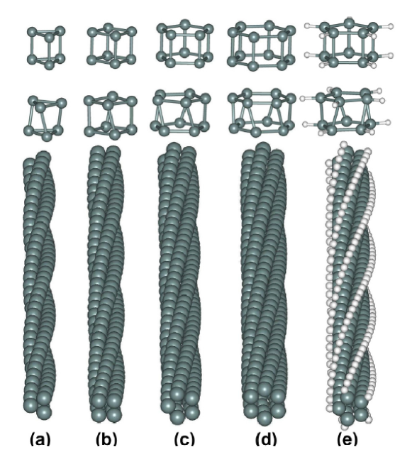
Figure 1 presents a schematic representation of the ultrathin twisted silicon nanowires studied here. We considered nanowires with several polygonal cross sections, containing three, four, five, or six silicon atoms. Based on the results of previous theoretical investigations, those structures are candidates to be energetically stable li ; sen ; justo2007 ; justo2007b . Structures with larger cross sections, i.e. containing more atoms in the rings, were found to be energetically less favorable than those structures presented here. It should be stressed that the systems investigated here can be classified as surface-like nanowire structures, which differ from bulk-like ones ma ; rurali , in which the nanowires have a large core (of at least 1 nm in diameter) with atoms in configurations equivalent to the respective ones in the crystalline phase. In the last case, the nanowire properties could be directly mapped to the respective properties in the crystalline phase. On the other hand, for the ultrathin nanowires investigated here, such mapping is not that direct.
Here, the twisting angle was defined as the angle formed between two equivalent atoms in neighboring silicon layers. Since we considered periodic boundary conditions in -direction, there was a limited number of possible intermediate twisting angles that could be effectively studied, which was directly associated to the number of wire layers in the simulation cell. Figure 2 presents the distance (in the direction) between two neighboring planes () as a function of the twisting angle for pristine nanowires. The results indicated that, for all wire types, the largest lattice parameter is associated to an untwisted configuration (0o). In that case, the lattice parameter is around 2.42 Å for all wire types, which is a little longer than the silicon interatomic distance in the crystalline diamond cubic phase (of 2.37 Å, computed within the same methodology and theoretical approximations mentioned in the previous paragraphs). This could be explained by the fact that, although silicon atoms in the nanowires are fourfold coordinated as atoms in the crystalline phase, they have angles between bonds that are far from the tetrahedral value, which causes important weakening on the silicon-silicon bonds, as compared to the ones in the crystalline phase.
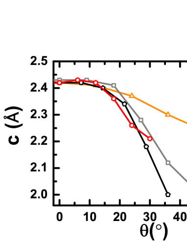
Twisting leads to a substantial lattice parameter shortening, by as much as 20 % (with respect to untwisted configurations) for the largest respective twisting angles, which corresponds, in the case of the pentagonal nanowire, to an angle of 36o. This lattice shortening, as a function of the twisting angle, comes simultaneously with large increase in the in-plane interatomic distances, , as summarized in table 1. For example, in the pentagonal nanowire with a twisting angle of 36o, increases by about 11% with respect to that in the untwisted configuration.
| shape | c | d(Si-Si) | /at | Y | |
|---|---|---|---|---|---|
| triangular | 0 | 2.415 | 2.418 | 0.172 | 1316 |
| 12 | 2.409 | 2.420 | 0.176 | 1277 | |
| 24 | 2.373 | 2.444 | 0.212 | 1153 | |
| 36 | 2.298 | 2.469 | 0.207 | 855 | |
| 48 | 2.238 | 2.477 | 0.201 | 417 | |
| 60 | 2.209 | 2.473 | 0.205 | 1336 | |
| square | 0 | 2.427 | 2.422 | 0.129 | 1300 |
| 9 | 2.434 | 2.428 | 0.131 | 1417 | |
| 18 | 2.413 | 2.440 | 0.182 | 1081 | |
| 27 | 2.277 | 2.508 | 0.200 | 1113 | |
| 36 | 2.119 | 2.581 | 0.147 | 1136 | |
| 45 | 2.024 | 2.641 | 0.085 | 1579 | |
| pentagonal | 0.0 | 2.421 | 2.405 | 0.00 | 2412 |
| pristine | 7.2 | 2.415 | 2.397 | 0.030 | 2098 |
| 14.4 | 2.397 | 2.405 | 0.106 | 1751 | |
| 21.6 | 2.337 | 2.424 | 0.147 | 1340 | |
| 28.8 | 2.182 | 2.531 | 0.157 | 921 | |
| 36.0 | 1.995 | 2.674 | 0.096 | 3422 | |
| pentagonal | 0.0 | 2.880 | 2.289 | 0.009 | 127 |
| passivated | 7.2 | 2.875 | 2.286 | 0.011 | 119 |
| 14.4 | 2.513 | 2.452 | 0.015 | 119 | |
| 21.6 | 2.481 | 2.418 | 0.006 | 114 | |
| 28.8 | 2.708 | 2.269 | 0.004 | 62 | |
| 36.0 | 2.651 | 2.258 | 0.00 | 76 | |
| hexagonal | 0 | 2.421 | 2.393 | 0.014 | 2809 |
| 6 | 2.433 | 2.390 | 0.035 | 2388 | |
| 12 | 2.421 | 2.398 | 0.112 | 1931 | |
| 18 | 2.355 | 2.419 | 0.143 | 1656 | |
| 24 | 2.262 | 2.437 | 0.151 | 1195 | |
| 30 | 2.205 | 2.474 | 0.150 | 1012 |
Figure 3(a) shows the nanowire relative total energy (per atom), in their pristine forms, as a function of the lattice parameter (for untwisted nanowires). The results indicated that nanowires present an elastic behavior for up to about 10 % of stretching deformation. The wires with pentagonal and hexagonal cross sections have the lowest energies, being the most stable ones, with a total energy of about 0.46 eV/atom higher than the value for silicon in a diamond cubic phase (computed using the same theoretical framework). Those results suggest that the nanowire configurations studied here are physically relevant, and have energies that are comparable or lower than the the ones in configurations studied elsewhere durgun ; palaria .
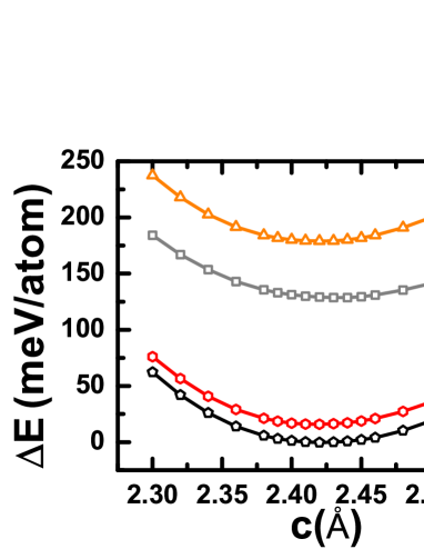
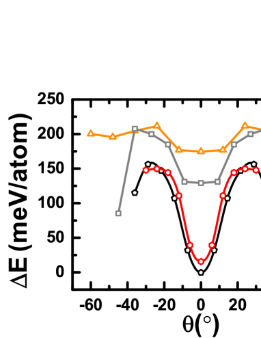
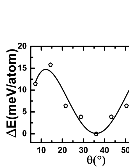
Figure 3(b) shows the nanowire relative total energy (per atom), in their pristine form, as a function of the twisting angle. The results indicated that, for a wire of any cross section, the equilibrium state was associated to an untwisted configuration. Additionally, the total energies of the pentagonal and hexagonal nanowires presented a parabolic behavior (as a function of the twisting angle), with an elastic limit which surpassed 100 of twisting. Therefore, ultrathin nanowires follow a Hooke’s law for torsion, even for large angles. For hydrogenated nanowires, we observed a considerably smaller twisting energy, as compared to the respective wires in their pristine forms. Additionally, the energy minimum of the hydrogenated nanowires were associated to twisted configurations. Therefore, hydrogenation drives a pristine nanowire on a spontaneous transition toward a twisted configuration. This result is consistent with what has been observed in several nanostructures, such as hydrogenation of graphene nanoribbons koskinen . Figure 4 shows the relative total energy of the hydrogenated pentagonal nanowire, with an equilibrium configuration at an angle of 360, and an elastic behavior for twisting angles around that minimum.
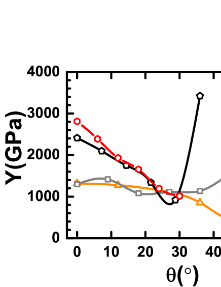
The nanowire elasticity is described by the Young’s modulus (). At a certain twisting angle, it is computed according to the respective curve of total energy as function of the deformation strain, as given in figure 3(a). This is obtained according to the expression , where E is the strain energy, is the axial strain, and is the equilibrium volume, defined as the product of axial equilibrium length () and the cross-sectional area () of a nanowire. For very thin nanowires, the definition of this area is very inaccurate, which can affect the results. In order to compute the Young’s modulus, each nanowire was slightly elongated and contracted (up to a few percents) from its equilibrium length , followed by full structural optimization lee . The Young’s modulus was then determined by a third-order polynomial expansion that fitted the calculated energy-strain curves. Table 1 presents the Young’s modulus of all the nanowires studied here. Figure 5 shows the Young’s modulus of nanowires, with all types of cross sections, as a function of the twisting angles. There is a general trend that the Young’s modulus decreases with increasing of the twisting angle, although for the pentagonal nanowire the Young’s modulus increases considerably for twisting angles beyond 300. This decrease in , as result of twisting, has its origin on the major changes on the chemical nature of inter-layer interatomic bonding. The values of the Young’s modulus could be compared to available data for those of ultrathin nanowires xia . The results for ultrathin nanowires in their pristine form are larger than the ones observed experimentally for several one dimensional nanostructures xia . For nanowires in their hydrogenated forms, as shown in figure 1(e), the Young’s modulus is considerably smaller than the respective ones in their pristine forms, as shown in table 1. Those values are consistent with results determined for hydrogenated nanowires zhu ; kang ; kou .
The results indicated that nanowires with pentagonal and hexagonal cross sections behave elastically for large twisting deformation, opening several possibilities for applications as electromechanical devices in nanometrology. It is particularly appealing to incorporate any type of silicon nanostructure, as a probe nanodevice, in an integrated circuit within the current silicon device technology garcia ; waggoner . An ultrathin nanowire could be used as a torsion nanobalance or electrometer, similar to macroscopic torsion balances which have been used to measure forces with great precision gund ; cleland . In fact, there is growing interest in developing devices to measure forces with precision below the 10 limit naka ; kramar2003 ; kim2010 ; gavartin .
Working as a electrometer resonator with the two ends fixed in a holder, the twisted nanowire would have a fundamental torsional resonance frequency (), which depends on the nanowire inertia moment () and the nanowire angular spring constant (). The angular spring constant, obtained from results presented in figure 3(b), is of the same order of the constant obtained for ultrathin Mo6S6 nanowires (where deformation was presented in terms of the twisting angle in deg/nm and potential energy in eV/nm). With the results from our calculations, presented in figure 3(b) and table 1, a pentagonal silicon nanowire in pristine form, with 20 layers and two fixed ends, would have a resonance frequency of the order of about 80 GHz. This frequency is considerably larger than the typical ones obtained in recent torsional experiments, in which micrometer-size paddles gave a resonance frequency of 2.61 MHz cleland , but consistent with the size effects.
Following the idea of measuring variations in the oscillating frequencies due to the presence of charged particles in the neighborhood of the twisting resonator paddle device cleland , a proper detection of frequency variations, for the silicon nanowires here investigated, could be hampered by thermal noise, even at very low temperatures. However, those ultrathin nanowires could have considerably smaller resonance frequencies, which would favor those measurements. Reducing such frequencies could be achieved by functionalizing the nanowires, such as by hydrogenation or anchoring other functional groups, which would reduce considerably the nanowire angular spring constant. Our results show that hydrogenation, as shown in figure 1(e), leads to a major decrease in the by almost an order of magnitude (according to results in figure 4), as compared to the same nanowire in a pristine form. The physical origin of this behavior is the major change on the chemical nature of silicon-silicon interactions as result of hydrogenation.
Our results suggest broad opportunities to obtain considerably high quality factors and sensitivity to measure charged systems in the nanowire neighborhood cleland . A twisted nanowire could be used as a device to measure torsions at nanoscopic level, with potential applications to study several molecular properties of DNA’s bryant . For a silicon pentagonal nanowire paddle with fixed ends, described in the previous paragraph, torsion of a few degrees could allow to explore torques and forces in the order of and 10 pN, respectively.
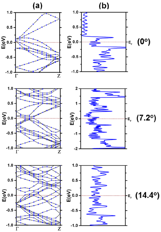
Our results indicate that the elastic properties of nanowires could be used to probe forces and torques at molecular level. The angular spring constant could be tailored to appropriate values for each application, by anchoring functional molecules in the nanowires. However, the major challenge would be how to translate the mechanical angular deformation of the nanowires in terms of macroscopic measurements. One of the most appealing possibilities is to explore the correlation between nanowire deformation and electronic transport, a nanowire property which is generally easily accessible appenzeller . In order to study the changes on the electronic properties of the nanowires as result of twisting, we computed the nanowire electronic band structures. Figure 6 presents the band structure of pentagonal nanowires, showing that the nanowires are metallic for all twisting angles. Several bands cross the Fermi level, which gives rise to a reasonably high density of states (DOS) in that region. On the other hand, there is a large increase on the density of states across the Fermi level as the torsion angle is increases, which would lead to an increase in the wire conductivity with increasing the twisting angle.
In summary, ultrathin twisted silicon nanowires, in pristine and hydrogenated forms, have been investigated as potential candidates for mechanical torsional nanodevices. All ultrathin nanowires followed a Hooke’s law for stretching and twisting, and such elastic properties could be explored to build nanoscopic torsion electrometers to measure forces and torques at molecular level. Additionally, the torsion properties could be tailored by functionalizing the nanowires. It should be stressed that nanowires of other materials, in pristine or functionalized forms, are also potential candidates to work as torsional electromechanical nanodevices.
Acknowledgements.
The authors acknowledge support from Brazilian Agencies FAPESP and CNPq. The calculations were performed at the computational facilities of LCCA of the University of São Paulo.References
- (1) Cui, Y., Wei, Q. Q., Park, H. K. , and Lieber, C. M., Science 293, 1289 (2001).
- (2) Hayden, O., Agarwal, R. , and Lieber, C. M., Nature Mater. 5, 352 (2006).
- (3) Lieber C. M. and Wang Z. L., MRS Bull., 32, 99 (2007).
- (4) Leach R. K., Claverley J., Giusca C., Jones C. W., Nimishakavi L., Sun W., Tedaldi M. , and Yacoot A., Meas. Sci. Technol. 23, 074002 (2012).
- (5) Comini E., Baratto C., Faglia G., Ferroni M., Vomiero A. , and Sberveglieri G., Progr. Mater. Sci. 54, 1 (2009).
- (6) Wang N., Cai Y. , and Zhang R. Q., Mater. Sci. Eng. R - Rep. 60, 1 (2008).
- (7) Cleland A. N. , and Roukes M. L., Nature (London) 392, 160 (1998).
- (8) Kim P. H., Doolin C., Hauer B. D., MacDonald A. J. R., Freeman M. R., Barclay P. E. , and Davis J. P., Appl. Phys. Lett. 102, 053102 (2013).
- (9) Cui, Y. , and Lieber, C. M., Science 291, 851 (2001).
- (10) Ma D. D. D., Lee C. S., Au F. C. K., Tong S. Y. , and Lee S. T. Science 299,1874 (2003).
- (11) Lauhon, L. J., Gudiksen, M. S. , and Lieber, C. M., Philos. Trans. R. Soc. Lond. A 362, 1247 (2004).
- (12) Hochbaum, A. I. et al., Nature 451, 163 (2008).
- (13) Rurali R., Rev. Mod. Phys. 82, 427 (2010)
- (14) Amato, M., Pauammo, M., Rurali, R. , and Ossicini, S., Chem. Rev. 114, 1371 (2014)
- (15) Sen P., Gulseren O., Yildirim T., Batra I. P. , and Ciraci S., Phys. Rev. B 65, 235433 (2002)
- (16) Xu F., Lu W. , and Zhu Y. ACS Nano 5, 672 (2011).
- (17) Popov I., Gemming S., Okano S., Ranjan N. , and Seifert G., Nano Lett.8, 4093 (2008)
- (18) Tizei L. H. G., Craven A. J., Zagonel L. F., Tencé M., Stéphan O., Chiaramonte T., Cotta M. A. , and Ugarte D., Phys. Rev. Lett. 107, 195503 (2001).
- (19) Akatyeva E. and Dumitric T., Phys. Rev. Lett.109, 035501 (2012).
- (20) Nakamura K. and Houk K. N., Organic Lett. 1, 2049 (1999).
- (21) Kresse G. and Furthmüller J., Phys. Rev. B 54, 11169 (1996).
- (22) Perdew J. P., Burke K. , and Ernzerhof M., Phys. Rev. Lett. 77, 3865 (1996).
- (23) Kresse G. and Joubert D., Phys. Rev. B 59, 1758 (1999).
- (24) Li B. X., Cao P. L., Zhang R. Q. , and Lee S. T., Phys. Rev. B 65, 125305 (2002).
- (25) Justo J. F., Menezes R. D. , and Assali L. V. C., Phys. Rev. B 75, 045303 (2007).
- (26) Menezes R. D., Justo J. F. , and Assali L. V. C., Phys. Status Solidi A 204, 951 (2007).
- (27) Durgun E., Çakir D., Akman N. , and Ciraci S., Phys. Rev. Lett. 99, 256806 ( 2007).
- (28) Palaria A., Klimeck G. , and Strachan A., Phys. Rev. B 78, 205315 (2008).
- (29) Koskinen P., Appl. Phys. Lett.99, 013105 ( 2011).
- (30) Lee B. and Rudd R. E., Phys. Rev. B 75, 195328 (2007).
- (31) Xia Y. N., Yang P. D., Sun Y. G., Wu Y. Y., Mayers B., Gates B., Yin Y. D., Kim F. , and Yan Y. Q., Adv. Mater. 15,353 (2003).
- (32) Zhu Y., Xu F., Qin Q., Fung W. Y. , and Lu W., Nano Letters 9, 3934 (2009).
- (33) Kang K. and Cai W., Int. J. Plast. 26, 1387 (2010).
- (34) Koukaras E. N., Niaz S., Zdetsis D. A. , and Zdetsis A. D., Microelectron. Eng. 90, 88 (2012).
- (35) Garcia J. C., de Lima D. B., Assali L. V. C. , and Justo J. F., J. Phys. Chem. C 115, 13242 (2011).
- (36) Waggoner P. S. and Craighead H. G., Lab on a Chip 7, 1238 (2007).
- (37) Gundlach J. H. and Merkowitz S. M, Phys. Rev. Lett.85, 2869 (2000).
- (38) Kramar A., Pratt J. R., Smith D. T. , and Williams E. R., IEEE Trans. Instrum. Meas. 52, 508 (2003).
- (39) Kim M. S. and Pratt J. R., Measurement 43, 169 (2010).
- (40) Gavartin E., Verlot P. , and Kippenberg T. J., Nature Nanotech. 7, 509 (2012).
- (41) Bryant Z., Stone M. D., Gore J., Smith S. B., Cozzarelli N. R. , and Bustamante C., Nature (London) 424, 338 (2003).
- (42) Appenzeller J., Knoch J., Bjork M. I., Riel H., Schmid H. , and Riess W., IEEE Trans. Electr. Dev. 55, 2827 (2008).