The Central Logic Board and its auxiliary boards for the optical module of the KM3NeT detector
Abstract
The KM3NeT neutrino telescope will be composed of many optical modules, each of them containing 31 (3") photomultipliers, connected to a Central Logic Board. The Central Logic Board integrates Time to Digital Converters that measure Time over Threshold of the photomultipliers signals while White Rabbit is used for the optical modules time synchronization. Auxiliary boards have also been designed and built in order to test and extend the performance of the Central Logic Board. The Central Logic Board, as well as the auxiliary boards, will be presented by focusing on the design consideration, prototyping issues and tests.
keywords:
Detector control systems (detector and experiment monitoring and slow-control systems, architecture, hardware, algorithms, databases); Digital electronic circuits1 Introduction
KM3NeT is a deep-sea research infrastructure, which will host a neutrino telescope with a volume of several cubic kilometres at the bottom of the Mediterranean Sea [1]. It will be composed by thousands of Digital Optical Modules (DOMs), consisting of a glass sphere containing 31 (3") PhotoMultiplier Tubes (PMTs) for the detection of the Cherenkov light induced by charged particles produced by the interaction of neutrinos with matter inside or in the vicinity of the KM3NeT detector [2, 3]. A group of 18 DOMs distributed over a 700 m mooring line constitutes a Detection Unit of the telescope.
The signal acquired by each photomultiplier is sent to a Time over Threshold (ToT) discriminator to fed the Time to Digital Converter (TDC) [4] which is part of a Central Logic Board (CLB) based on the Kintex 7 FPGA. The TDC resolution is 1 ns and the White Rabbit technology [5] is used to guarantee time synchronization at the level of 1 ns between each DOM.
Additional peripheral devices are connected to the CLB, in order to keep track of both the environmental conditions (temperature, humidity), the DOM orientation (yaw, pitch, roll) and its position; some of them are embedded on the board, such as the temperature & humidity sensor and the tiltmeter & compass, while others are plugged to the CLB by using connectors, such as the acoustic devices (Piezo or Hydrophone) and the Nanobeacon (a LED device). Custom boards have also been designed and produced to test the performances of the CLB or to extend its functionalities.
All the incoming data are collected by the CLB and sent to shore using a dedicated optical network. Two Lattice Microcontrollers 32-bit (LM32) [6] are implemented in the CLB FPGA, one for the White Rabbit and the other for the instrumentation management.
Two batches of prototypes have been produced and are now operational in the laboratories of the KM3NeT Collaboration; 60 pieces were ordered to equip the first two KM3NeT Detection Units which will be deployed during 2015. A prototype Detection Unit [7] has been deployed in May 2014 at the KM3NeT-It installation site 100 km SE off shore of Capo Passero, Sicily, and it is continuously taking data since its connection to the on-shore station.
2 The Central Logic Board
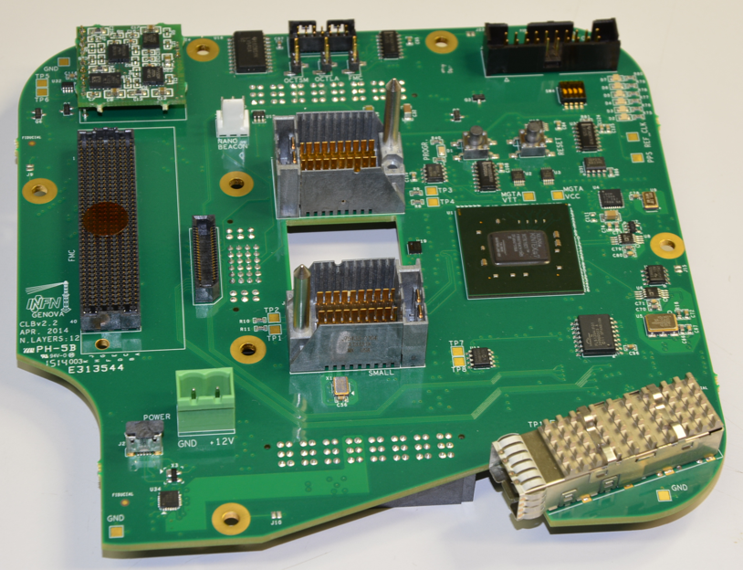
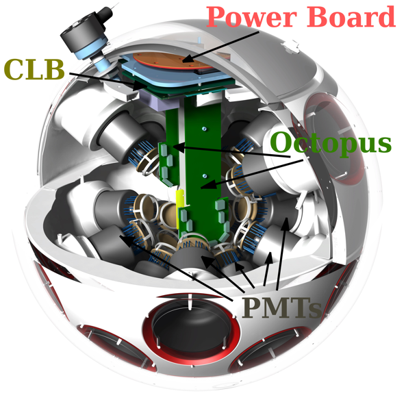
The CLB, showed in figure 1, is the main logic board of the KM3NeT DOM (see figure 2). It is directly connected with a Power Conversion Board which provides all the needed rails for the board (1.0 V, 1.8 V, 2.5 V, 3.3 V, 5.0 V). The purpose of the CLB is to manage all the instrumentation present inside the DOM, acquire incoming data from the 31 PMTs and from the acoustic device, pack the data into User Datagram Protocol (UDP) packets and send them through the optical line. A time synchronization of 1 ns level between all the DOMs is achieved by the usage of White Rabbit.
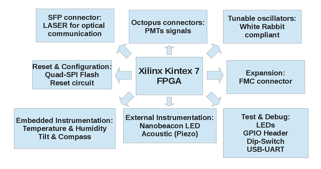
A schematic block of the CLB is shown in figure 3. It is based on a Xilinx Kintex 7 FPGA, which is connected to all the rest of the board, including in particular:
-
•
1 Small Form-factor Pluggable (SFP) connector for the optical communication
-
•
2 custom Octopus connectors for the PMTs signals
-
•
Tunable oscillators (White Rabbit compliant)
-
•
Embedded instrumentations (temperature and humidity sensor, tilt & compass)
-
•
External connectors (for Nanobeacon LED, acoustic device, expansion boards)
3 The firmware
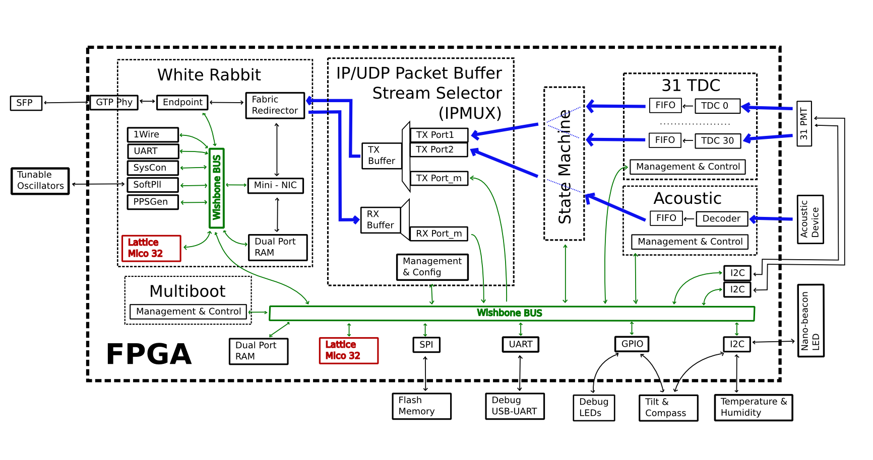
The firmware of the CLB (see figure 4) is based on two LM32; Wishbone buses are used to interconnect the microcontrollers with all the other Intellectual Property cores. Part of the firmware is dedicated to the White Rabbit (left in the figure), which directly manages the tunable oscillators and the optical link, in order to achieve a time synchronization of sub-nanosecond level with the Grand Master clock of the on-shore station. All the rest of the board is managed by the second microcontroller, which has access to all the drivers (SPI, UART, GPIO and I2C) needed for the instrumentation, the configuration and the test of the board.
A multiboot module allows the selection of a different image from where to boot the FPGA, and the presence of a Golden Image as a fallback solution, will make possible to remotely update the firmware after the deployment of the DOM.
An acoustic module is dedicated to the decoding of the incoming AES3 formatted stream, while 31 TDCs are responsible to record the timestamp and the width (with 1 ns of resolution) of hits incoming from the ToT signals of the PMTs. All the data, together with some other slow control monitoring information (as temperature, humidity, tilt & compass, currents, …) are put in UDP packets by a state machine, and sent to the IPMUX module, the responsible for the management of the transmission and reception of packets to/from the on-shore station.
4 The layout
The CLB layout is composed of 12 layer, with:
-
•
Six Signal layers including top and bottom
-
•
Two Power planes
-
•
Four ground planes
The layers are symmetrically disposed around the 2 Alimentation layers; ground planes are positioned at the sides of the signal layers to have better signal integrity, as well as a limited number of vias was used. Particular attention was put on the differential pairs routing keeping the time difference of less than 100 ps between different PMT signals, and less than 20 ps between clock signals.
A reliability analysis using the FIDES method [8] was performed, showing an estimated risk for failure of less than 10 % after 15 years.
Several signal integrity simulation were performed on different signals on the board, always showing a good level discrimination.
5 Tests
Several tests have been done on the CLB by the electronic group of the KM3NeT collaboration. The tests covered all the functionality of the board, and where performed separately, by focusing on the dedicated hardware and firmware section. Currently integration tests with a full assembled DOM are undergoing, and all the functionalities of the DOM are enabled.
The first and most important tests are about the time synchronization and the optical communication link; the White Rabbit section of the firmware and hardware were tested by connecting a CLB with a Simple PCIe FMC carrier card. The two boards used the White Rabbit Precision Time Protocol to achieve a sub-nanosecond level time synchronization, showed on the oscilloscope by using a pulse per second output signal from both the two boards. Other tests, with more boards involved and White Rabbit switches used to simulate the final topology of the KM3NeT network followed.
The second test regarded the PMT signals acquisition. Using a pattern generator plugged on the Octopus connector of the CLB, a regular pattern was sent to simulate all the 31 signals and the TDCs in the FPGA firmware were tested, together with the UDP packet building and sending systems. Results were analyzed by software applications on PC directly connected to the optical line of the CLB. Then more tests followed, by using real PMTs, connected through the Octopus boards and putted in a dark box. Hit rates were analyzed in different conditions of high voltage and threshold settings for the ToT measurement.
Then the acoustic module was tested by plugging a prototype of the final acoustic device to the CLB and sending the decoded data to a PC using the UDP packet transmission; the multiboot module was tested as well, and all the instrumentation on the board were tested by using a shell command interface with the USB-UART connection implemented in the software embedded, before redirecting all the data output to the optical line.
A thermal analysis was also performed on the board, showing two hot regions near the FPGA and near the SFP connector, having in both case a maximum temperature of about 40 ∘C. A second measurement has been performed by inserting the CLB and the Power Board in the final mechanical structure, which act as a dissipator, and the temperature on the CLB was found decreased by about 10 C. Only the core of the FPGA reached 50 ∘C.
Finally an Electromagnetic Interference analysis was performed on the CLB with the Power Board plugged below it. The results showed the presence of two hot spots in the center of the boards, due to DC-DC converters on the Power Board; a second measurement was done by inserting a metal plane between the two boards, as it will be in the final design, and the two spots were not present anymore. A third hot spot was found on the top of the CLB, due to a test signal that will not be active during normal operation.
6 Auxiliary boards
The KM3NeT detector foresees to use the CLB not only inside the DOM, but also in the Detection Unit Base and in the Calibration Unit. Here the CLB functionalities will be slightly different from the standard one, for example no PMT measurements will be done, but the control of other instrumentation will be required.
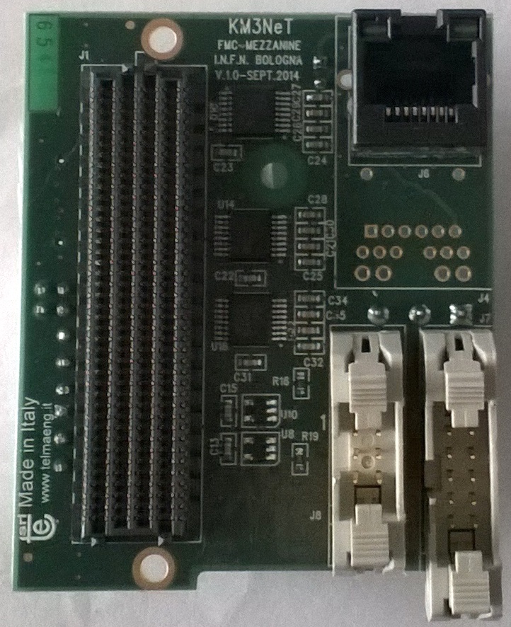
In order to make all the needed connections available to the CLB, a FPGA Mezzanine Card (FMC) Expansion Board (see figure 5) has been designed and produced; in particular, small dimensions are required to fit in the mechanical constraints of the base modules. The Expansion Board provides the following additional ports:
-
•
3 additional RS232 ports
-
•
2 trigger lines with the RS485 standard
-
•
1 additional acoustic interface, using an RJ45 connector
The serial ports are used to communicate with dedicated slow control instrumentation installed in the Detection Unit base and in the Calibration Unit. The additional RS485 serial lines are required to trigger a laser emitter and an acoustic emitter used for the calibration of the KM3NeT detector; the acoustic interface is required for a more sensitive device than the one inserted in each DOM, that will be used for scientific studies in different fields, including physics and marine biology.
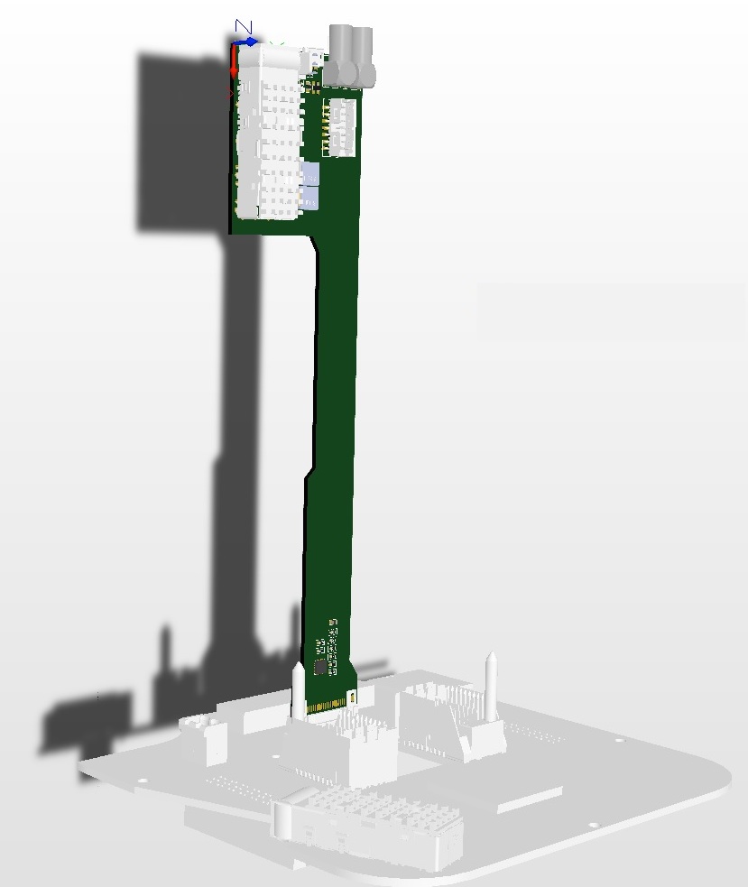
An additional auxiliary board (the so-called “G” Board) have been designed to allow testing and debugging of the CLB when it is assembled inside the full (or half) DOM. In this situation, in fact, the space inside the DOM will be really crowded because of the presence of the 31 PMTs; the CLB will not be accessible anymore, except using the optical line. This could not be sufficient during the test phase, hence the “G” Board will be used, by inserting it with care in the DOM and plugging it to the CLB, as shown in figure 6.
This board allows the access to basic test functionalities as:
-
•
JTAG chain
-
•
USB ports
-
•
LEMO connectors for the timing synchronization (Clock and Pulse Per Second signals)
-
•
SFP connector to be used in case of problems with the one on the CLB
7 Conclusions
The Central Logic Board is responsible of the management of the Digital Optical Module of the KM3NeT detector. It has to acquire data from 31 PMTs, from one acoustic device and from other monitoring instrumentation, put them in UDP packets and send them to the On-Shore station. A time sinchronization of the sub-nanosecond level between all the KM3NeT DOMs is achieved by using White Rabbit.
The electronic group of the KM3NeT collaboration took care of the design, analysis and test of the CLB and its auxiliary boards, needed to expand its functionalities or for testing purposes.
Two series of prototypes were built, the first of 6 pieces and the second of 12 pieces. Than a pre-serie production of 22 boards followed. Currently it is in production a new batch of 60 boards, and a mass production of 540 boards is expected by the end of the 2014.
References
- [1] \hrefhttp://www.km3net.org The KM3NeT detector web site
- [2] S. Adrián-Martínez et al., Expansion cone for the 3-inch PMTs of the KM3NeT Optical Modules, JINST 8 (2013) T03006.
- [3] S. Adrián-Martínez et al., Deep sea tests of a prototype of the KM3NeT digital optical module, Eur. Phys. J. C 74 (2014) 3056.
- [4] D. Calvo, High-Resolution Time To Digital Converters for the KM3NeT Neutrino Telescope, Proceedings for the TWEPP 2014, to be published in JINST.
- [5] \hrefhttp://www.ohwr.org/projects/wr-cores/wiki/wrpc_core The White Rabbit web site
- [6] \hrefhttp://www.latticesemi.com/en/Products/DesignSoftwareAndIP/IntellectualProperty/IPCore/IPCores02/LatticeMico32.aspx The LM32 web site
- [7] S. Biagi, Operation and results of the prototype KM3NeT detection unit, Proceedings for the RICAP 2014, to be published in EPJ Web of Conferences.
- [8] \hrefhttp://fides-reliability.org The FIDES web site