Study of the hidden-order of URu2Si2 by point contact tunnel junctions.
Abstract
URu2Si2 presents superconductivity at temperatures below 1.5 K, and a hidden order (HO) at about 17.5 K, both electronic phenomena are influenced by Fano and Kondo resonances. At 17.5 K the HO was related in the past to a Peierls distortion that produces an energy gap deformed by the resonances. This order has been studied by more than 20 years, still without a clear understanding. In this work we studied the electronic characteristics of URu2Si2 in a single crystal, with tunneling and metallic point contact spectroscopies. In the superconducting state, we determined the energy gap, which shows the influence of the Fano and Kondo resonances. At temperatures where HO is observed, the tunnel junctions spectra show the influence of the two resonances. Tunnel junctions characteristics show that the Fermi surface nesting depends on the crystallographic direction.
I Introduction
URu2Si2, is one of the most studied materials, after more than 20 years the electronic characteristics are still not well understood. One notable example is the so called hidden order which remains unexplained. Transport measurements in this compound have shown many details related with the general behavior; from room temperature to 70 K URu2Si2 presents a characteristic typical of a Kondo system associated to the interaction of heavy electrons and conducting electrons. With a Kondo lattice formed at 70 K haule09 ; chatterjee13 , below this temperature the resistivity dramatically drops, and at K an anomaly is observed. In the past this was related to a spin density wave (SDW). However this feature is called the Hidden Order (HO). It presents many diverse electronic characteristics that modifies other occurring proceses L.Buyers ; P.Chandra ; Oh ; mydosh . At lower temperature below 1.5 K the compound, turns into a superconducting state which many researchers believe must be anomalous in the sense that does not follow the BCS model maple ; ramirez ; ohkuni ; kwok ; moyoyama ; hassinger .
As mentioned before the HO was associated in the past to a Peierls distortion, but careful experiments carried out to detect the Peierls (SDW) distortion did not find any magnetic order, only a quite small staggering magnetism, probably related to magnetic impurities, not related to SDW behavior. This absences imply that the gaping on the Fermi surface may be related to another unknown electronic phenomena L.Buyers ; Broholm . Actually, doubts still persist about the physics behind the anomalies at about 17.5 K. The HO changes transport, and thermal properties, and opens an energy gap, and altering the superconducting behavior Oh ; M.Palstra ; mydosh ; ramirez ; deVisser ; U.Walter ; Mason . The occurrences of the HO, and the relationship with the Fano and Kondo resonances is not completely understood, nobody knows the influence of the two resonances and how those are affecting the general behavior, for instances the manner that the Kondo lattice at high temperature and the resulting distortion at 17 K modifies the electronic characteristics. Experiments with very sensitive techniques as tunneling and point contact spectroscopy (PCS) provide the observation of the Fano resonance that distorted the feature of the energy gap, at K as observed by Schmidt, et al, with Scanning Tunneling Spectroscopy schmidt .
Many researchers who investigated this transition demonstrated that this is a second order thermodynamic transition maple ; ohkuni ; escudero ; morales ; schlabitz . The effects of the resonances at the transition show the consequence of a partial electronic screening that modifies the transport and thermal properties because the strong hybridization between conducting electrons and heavy localized electrons schmidt ; aynajian . The result of all those processes is that the Kondo and Fano lattices are spatially modulates. The signature of these lattices are displayed as modifications at the Fermi surface. Thus, portions of the Fermi surface at high and low temperatures are distorted and observed with many experimental tests and theoretical studies haule09 ; maple ; villaume ; chandra ; rodrigo .
This work shows our new experimental observations obtained with techniques that give additional information about the features and characteristics of this compound using tunneling and PCS IvarG ; IvarGi ; K.Yanson ; A.Duif ; Jansen .
The studies at high temperatures from 40 to 1.7 K were performed using tunnel junctions to observe the HO that develops at 17.5 K. We studied the anomalous features of the gap, using a well characterized URu2Si2 single crystal escudero ; morales ; hass , we measured the spectroscopic characteristics of the crystal in two crystallographic directions.
At lower temperature the superconducting state was studied with metallic point contacts (PCS) in the range of temperatures where superconductivity develops, the studies were performed from 2.5 to 0.3 K. PCS junctions were in the diffusive limit but close to the ballistic regime. In all experiments, here reported, from 40 K to 0.3 K the influence of the Fano and Kondo resonances was observed. In the superconducting state the influence of both resonances was clearly evidenced; the feature of the energy gap was completely distorted, and the effect of these resonances is clearly noted when examined the evolution with temperature of the energy gap.
In the range of temperatures where HO is set, the influence was studied in two directions of the crystal, the Fano features are different in both directions.
This work reports tunneling and point contact experiments performed in URu2Si2 single crystals. At temperatures from 1.7 K to 40 K, tunneling spectroscopy shows the effect of the Fano and Kondo resonances on the energy gap, and the dependence on the crystallographic direction. The energy gap in the direction is bigger than the gap in the direction. In the superconducting state, with PCS we found that the energy gap as a function of temperature follows the BCS prediction after the Fano anomaly is subtracted from the differential conductance.
II Experimental details
The URu2Si2 single crystals used in this study were growth by Czochralski method and annealed for one week at 850∘ C. They have similar characteristics to that reported elsewhere hass ; morales ; escudero . The crystals have a platelet-like shape with the crystallographic axis perpendicular to the plane of the platelet, typical dimension of the used crystals were about 2x3x0.5 mm3.
The samples were characterized by resistance as a function of temperature measurements. The applied current was 100 A. The resistance ratio between room temperature and low temperature resistance R(300 K)/R(2 K)=38. The anomaly associated to the HO is observed clearly at about 17.5 K. At lower temperature, the superconducting transition temperature is at =1.37 K (R=0), this transition is also similar to the observed in other experiments by other researchers. The transition temperature width was 0.15 K. Two type of junctions were formed, tunnel junctions were build by using a tip of Au(W) wire and the URu2Si2 crystal. The insulating barrier that forms the tunnel junction was the native oxide on the surface of the compound, and/or the oxide on the tip of the wire. The reason to assume that the junctions in our experiments behaves as tunnel or point contacts is the oxide formed in the wire or the sample, two considerations we have for this behavior; the shape of the differential conductance - bias voltage shows a typical curve of a tunnel junction akerman . In tunnel junctions the zero bias minimum in the curves is displaced out of the origin. Aspect quite different to a metallic contact junction, where the minimum in the differential conductance always occurs at zero bias voltage akerman . However another important consideration is the value of the differential resistance at zero bias, in our tunnel junctions, this is of the order about 20 - 50 . Several try outs were performed until reproducible data was obtained. Junctions with differential resistances at zero bias voltage between 2050 gives the most reproducible data. The two crystallographic directions of single crystal were measured with the prepared tunnel junctions; one used to measure over the edge of the crystal axis, the direction, and the another on the plane of the platelet axis. For the measurements and characterization of the superconducting state, point contact junctions were used. These were formed with the single crystal and a fine tungsten-gold tip with diameter on the tip, smaller than 5 m, those junctions were prepared at room temperature and glued to a glass substrate with Oxford varnish. The area of the junctions were estimated to be 1 m2.
The differential resistance d/d as a function of the bias voltage of the point contacts was measured with the standard modulation ac lock-in amplifier technique, and bridge. The temperature range for characterization of the superconducting state was from 0.325 to about 3 K. For characterization of the hidden order the temperatures range was from 1.7 K to 40 K using a MPMS system from Quantum Design as cryostat, whereas below 2 K a 3He Oxford refrigerator was used.
The characterization of the work regime of the point contacts was estimated with the Wexler’s interpolation formula wexler ; we substituted the mean free electronic path Å hass , the resistivity 40 -cm measured at 2 K rauch and the resistance of the point contacts measured at zero bias voltage. The obtained radii values, between 320 Åand 3700 Å, indicate that the contacts are in the diffuse regime, but not far to the ballistic duif .
An important aspect of the junctions used was the thermal stability. In this work we report studies performed in more than 20 different contact junctions, all shown similar curves.
III Results and discussion
Temperature evolution of the differential conductance versus bias voltage from 1.7 to 14.5 K are presented in Fig.1. These curves reveal the spectroscopic features of the Fano and Kondo resonances, measured in the crystalline direction. The spectroscopic features of the Fermi surface and the density of states are strongly modified by the Fano and Kondo lattices. Note that in a Peierls distortion the effects are quite different.
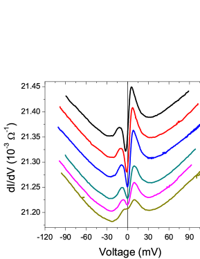
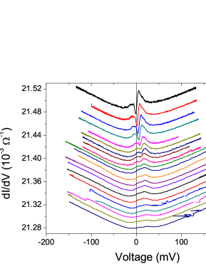
The evolution of the spectroscopic features, when temperature is increased, decreases the distortion in the differential conductance. Only close to T = 17.5 K where the hidden order develops the distortion is very small. Fig. 2 shows measures performed from 1.7 K to 26 K, in direction of the crystal, the distortion decreases as the temperature increases, but it persists at high temperature, the curves measured of the differential conductance characteristic at 1.7 K show a typical Fano resonance shape, with very sharp structure. Those characteristics were also observed with similar detail by Elgazzar, et al. and Aynajian, et al. aynajian ; elga . One set of measurements in the same direction, , up to 40 K, shown in Fig. 3, displays the typical parabolic background of a normal tunnel junction, with the conductance minimum shifted from the zero bias voltage, out of the origin wolf . However, close examination of the curves still indicates that some features persist at bias voltages at 2545 mV. Those features may be related to the Kondo lattice.
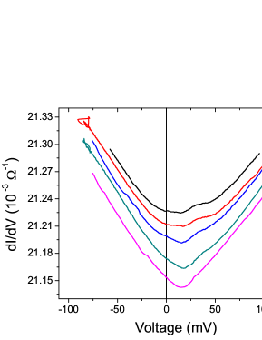
Fig. 3 shows the smoothing of the central peak and the displacement of the minimum out of the origin. However, also the normal parabolic shape of a tunnel junction is noted, but with very small structure wolf perhaps because the remanence of the Kondo lattice. Summarizing, Figure 2 and 3 shows the effect of temperature on the features around zero bias that we are attributed to the formation of a possible arising of a hybridization gap by the Kondo lattice at temperatures for above 70 K park12 . In Figure 4 we show data measured in the crystallographical direction, these data measured from 20 to 2 K. The spectra are different to the measurements in direction, in the direction the differential conductance shows two peaks at mV, which tends to decrease as the temperature was increased. At 20 K there is no distortion. Note that the Fano anomaly looks completely different to the observed in the direction. The data was measured and was reproducible when measured in different junctions. This Fano distortion is different to as the Fano theoretical model fano . Figure 4 shows two peaks in the differential conductance, these are quite symmetrical with similar magnitude. Those peaks observed at 2 K, are separated from the origin at 10 mV, we may consider that the difference of voltage between the peaks may be the size of an energy ”gap” of the HO, big, as the gaping in direction maple . Similarly as in other figures and directions, figure 4 shows a decreasing structure, tending to be smoothed as temperature is increased. This structure disappears at 20 K. We noted that in direction no structure exist at 20 K, but in direction still remains. This is in agreement with the observations by Haule and Kotliar in U or Si site haule09 . Also we have to mention that in total accord with Park et al. park12 the new features of the Fano resonance, as observed in Fig. 4 with measurements taken in the crystallographic direction of our sample, clearly may indicate another type of a Fano resonance and/or feature of a hybridization gap.
Our experiments, show that nesting depends on the crystallographic direction, and this may be related to size of the HO gap. Measurements in direction show that 2= 20 mV, which is small in , as already determined by Aynajian et al. as 8 mV aynajian . With the analysis of the characteristics at temperatures from 40 to 1.7 K, measured in the direction is possible to do a determination of the HO gap; at 2 K the two maxima are 10 mV, and the ratio 2/KBTC is 13.
Point contact experiments reported by Naidyuk et al. naidyuk ; naidyuk96 , from temperatures above the superconducting transition up to 20 K, show the differential conductance as a function of bias voltage measured in the direction and perpendicular to it. In those experiments the features observed in the direction are not show, meanwhile in the direction an energy gap is observed with a value about 10 mV, but no features were observed above 17.5 K. Our experiments reported here show features up to 40 K. As mentioned above this behavior over 17.5 K might be interpreted as the arising of a hybridization gap by normalized bands park12 . Our measurements, in the direction, display more structures which may be associated to an energy gap, persisting above 17.5 K up to 40 K in agreement to Park et al. park12 .
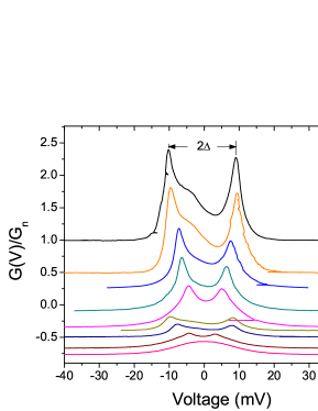
Studies with PCS were performed at low temperature in the superconducting state to see the evolution with temperature of the energy gap. The features were characterized from 3 K to 0.325 K using a 3He as cryostat. In Figure 5A we show the differential conductance between 0.325 K and 1.7 K, all curves were displaced in the vertical direction by a small amount to have a clear view and details. At temperatures above the superconducting state the Fano resonance may be observed as a distortion at the central part of the curves at zero bias voltage, this behavior was observed and analyzed when plotting the evolution of the gap with temperature. At the lower accessible temperature the superconducting gap feature is well formed, in panel B of figure 5 we display and plot temperature evolution of the gap.
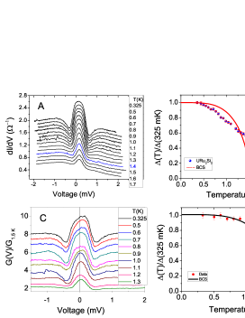
As show in Fig. 5B the energy gap evolution does not follows the BCS model (see continuous line). This anomalous behavior morales is the effect of the Fano and Kondo resonances. In Fig. 5C it is presented the normalized differential conductance of the same PCS with the structure related to the Fano resonance subtracted in all data. The subtracted data was the differential conductance measured at 1.7 K. The data substraction was performed in a similar manner as performed by Aynajian et al. aynajian . Fig. 5 panel D presents the results of this procedure. Data of the superconducting gap as a function of temperature now clearly follow BCS. The characteristics shown in Fig. 5B and 5D, show the influence of the resonances in the evolution with temperature of the gap. Our measurements also indicate that the ratio 2/KBTC is 7.86 -7.57. with the transition temperature between 1.35 - 1.4 K, this value is characteristic of a strong coupling superconductor. However, it is very important to mention that recent studies by Kawasaki et al., and Schemm et al. kawa ; schemm have shown time reversal symmetry breaking, using different experimental techniques. Kawasaki, et al, studied the HO and superconductivity using muon spin relaxation spectroscopy, whereas Schemm, et al. using Kerr effect. Both experiments found evidence of broken time reversal symmetry, which has a strong implication for both phenomena occurring in URu2Si2. Some features below the superconducting state, performed with polar Kerr experiments were observed and as suggested by Schemm et al. this effects may imply other physical processes in the superconducting state, and well above in the HO phase at 25 K schemm . Therefore, as mentioned by Kawasaki et al. and Schemm et al., those observations may imply a novel pairing mechanism for the superconducting behavior.
IV Conclusions
In summary, we have studied the electronic characteristics of URu2Si2 with tunnel and point contacts spectroscopies. The spectra show a gap feature with distortions because Fano and Kondo resonances, at high and low temperatures. At low temperature the superconducting gap has an anomalous evolution with temperature. From 0.3 to 2.4 K, we found the influence of the Fano and Kondo resonances and were subtracted, then energy gap follows BCS. From 1.7 to 40 K we observed the presence of the resonances that distorted the features on the Fermi surface, those look different in different crystallographic directions. Lastly, in the direction the structure in the differential conductance persists up to 40 K, whereas in the direction it persists up to 20 K. The HO effects are different in both directions of the Fermi surface.
Acknowledgements.
This work was partially supported by the Dirección General de Asuntos del Personal Académico, UNAM, project IN106414; by Consejo Nacional de Ciencia y Tecnología, (CONACyT), project 129293, (Ciencia Básica), BISNANO of the European Community and México, and project PICCO 11-7 by the Instituto de Ciencias del Distrito Federal, Cd. de México.References
- (1) Haule K and Kotliar G 2009 Nature Phys. 5 796
- (2) Chatterjee S, Trinckauf J, Hänke T, Shai D E, Harter J W, Williams T J, Luke G M, Shen K M, and Geck J 2013 Phys. Rev. Lett. 110 186401
- (3) Buyers W J L 1996 Physica B 223&224 9
- (4) Chandra P, Coleman P, Mydosh J A, Tripathi V 2002 Nature 417 831
- (5) Oh Y S, Kim K H, Sharma P A, Harrison N, Amitsuka H, and Mydosh J A 2007 Phys. Rev.Lett. 98 016401
- (6) Mydosh J A, Oppeneer P M 2011 Rev. Mod. Phys. 83 1301
- (7) Maple M B, Chen J W, Dalichaouch Y, Kohara T, Rossel C, Torikachvili M S, McElfresh M W, and J. D. Thompson J D 1986 Phys. Rev. Lett. 56 185
- (8) Ramirez A P, Coleman P, Chandra P, Bruck E, Menovsky A A, Fisk Z, and Bucher E 1992 Phys. Rev. Lett. 68 2680
- (9) Ohkuni H, Ishida T, Inada Y, Haga Y Yamamoto E, Onuki Y, and Takahasi S 1997 J. Phys. Soc. Jpn. 66 945
- (10) Kwok W K, DeLong L E, Crabtree G W, Hinks D G, and Joynt R 1990 Phys. Rev. B 41 11649
- (11) Motoyama G, Nishioka T, and Sato N K 2003 Phys. Rev. Lett. 90 166402
- (12) Hassinger E, Knebel G, Izawa K, Lejay P, Salce B, and Flouquet J 2008 Phys. Rev. B 77 115117
- (13) Broholm C, Lin H, Matthews P T, Mason T E, Buyers W J L, Collins M F, Menovsky A A, Mydosh J A, Kjems J K 1991 Phys. Rev. B 43 12809
- (14) Palstra T T M, Menovsky A A, and Mydosh J A 1986 Phys. Rev. B 33 6527
- (15) de Visser A, Kayzel F E, Menovsky A A, Franse J J M, van den Berg J, and Nieuwenhuys G J 1986 Phys. Rev. B 34 8168
- (16) Walter U, Loong C-K, Loewenhaupt M, and Schlabitz W 1986 Phys. Rev. B 33 7875
- (17) Mason T E and Buyers W J L 1991 Phys. Rev. B 43 11471
- (18) Schmidt A R, Hamidian M H, Wahl P, Meier F, Balatsky A V, Garrett J D, Williams T J, Luke G M, and Davis J C 2010 Nature 465 570
- (19) Escudero R, Morales F, and Lejay P 1994 Phys. Rev. B. 49 15271
- (20) Morales F and Escudero R 2009 J. Low Temp. Phys. 154 68
- (21) Schlabitz W, Baumann J, Pollit B, Rauchschwalbe U, Mayer H M, Ahlheim U, and Bredl C D 1986 Z Phys. B 62 171
- (22) Aynajian P, da Silva Neto E H, Parker C V, Huang Y, Pasupathy A, Mydosh J, and Yazdani A 2010 Proc. Natl. Aacad. Sci. 107 10383
- (23) Villaume A, Bourdarot F, Hassinger E, Raymond S, Taufour V, Aoki D, and Flouquet J 2008 Phys. Rev. B. 78 012504
- (24) Chandra P, Coleman P, Mydosh J A, and Tripathi V 2002 Nature 417 831
- (25) Rodrigo J G, Guinea F, Vieira S, and Aliev F G 1997 Phys. Rev. B 55 14318
- (26) Giaever I 1960 Phys. Rev. Lett 5 147
- (27) Giaever I and Megerle K 1961 Phys. Rev. lett. 5 1101
- (28) Yanson I K, Kulik, I O and Batrak A G 1981 J. Low Temp. Phys. 42 527
- (29) Duif A M, Jansen A G M and Wyder P 1989 J. Phys.: Condens. Matter. l 3157
- (30) Jansen A G M, van Gelder A P and Wyder P 1980 J. Phys. C: Solid St. Phys. 13 6063
- (31) Hasselbach K, Kirtley J R, and Lejay P 1992 Phys. Rev. B. 46 5826
- (32) Jönsson-Åkerman B J, Escudero R, Leighton C, Kim S, and Schuller I K 2000 Appl. Phys. Lett. 77 1870
- (33) Wexler G 1966 Proc. Phys. Soc. 89 927
- (34) Rauchschwalbe U 1987 Physica B 147 1
- (35) Duif A M, Jansen A G M and Wyder P 1989 J. Phys.: Condens. Matter 1 3157
- (36) Elgazzar S, Rusz J, Amft M, Oppeneer P M and Mydosh J A 2009 Nat. Mat. 8 337
- (37) Wolf E L 1989 Principles of electron tunneling spectroscopy (Oxford University Press: New York)
- (38) Park W K, Tobash P H, Ronning F, Bauer E D, Sarrao J L, Thompson J D, and Greene L H 2012 Phys. Rev. Lett. 108 246403
- (39) Fano U 1961 Phys. Rev. 124 1866
- (40) Naidyuk Y G, Kvitnitskaya O E, Yanson I K, Nowack A, and Menovsky A A 1995 Low Temp. Phys. 21 236
- (41) Naidyuk y G, Kvitnitskaya O E, Nowack A, Yanson I K, Menovsky A A 1996 Physica B 218 157
- (42) Blonder G E, Tinkham M, and Klapwijk T M 1982 Phys. Rev. B. 25 4515
- (43) Kawasaki I, Watanabe I, Hillier A, and Aoki D 2014 J. Phys. Soc. Jpn. 83 094720
- (44) Schemm E R, Baumbach R E, Tobash P H, Ronning F, Bauer E D, and Kapitulnik A 2014 arXiv: 1410.1479v1