Efficient spin injection into graphene through a tunnel barrier: overcoming the spin conductance mismatch
Abstract
Employing first-principles calculations, we investigate efficiency of spin injection from a ferromagnetic (FM) electrode (Ni) into graphene and possible enhancement by using a barrier between the electrode and graphene. Three types of barriers, -BN, Cu(111), and graphite, of various thickness (0-3 layers) are considered and the electrically biased conductance of the Ni/Barrier/Graphene junction are calculated. It is found that the minority spin transport channel of graphene can be strongly suppressed by the insulating -BN barrier, resulting in a high spin injection efficiency. On the other hand, the calculated spin injection efficiencies of Ni/Cu/Graphene and Ni/Graphite/Graphene junctions are low, due to the spin conductance mismatch. Further examination on the electronic structure of the system reveals that the high spin injection efficiency in the presence of a tunnel barrier is due to its asymmetric effects on the two spin states of graphene.
pacs:
72.80.Vp, 71.15.Mb, 73.40.Ns, 85.75.-dI INTRODUCTION
In the last decade, graphene has been the focus of intensive materials research due to its potential applications in many areas.Geim and Novoselov (2007) Because of the weak spin-orbital coupling in carbon system, graphene has long spin relaxation time and long spin diffusion length, which underlies the potential application of graphene in spintronics. A key step for realizing graphene-based spintronic devices is injection of a spin current into graphene and which has been the focus of many studies. The first work on spin transport in graphene was reported in 2006 by Hill et al.Hill et al. (2006) Using ferromagnetic (FM) NiFe electrodes, they observed a spin valve effect, in which a spin-polarized current injected from one ferromagnetic electrode, goes through graphene before being detected at the other electrode. This idea was soon pursued by several other groups.Han et al. (2009); Tombros et al. (2007); Popinciuc et al. (2009); Goto et al. (2008) However, the reported spin injection efficiency, a key parameter for spin transport, was only about 1 % if graphene is directly in contact with the FM leads.Hill et al. (2006); Han et al. (2009); Goto et al. (2008) The low spin injection efficiency is mainly due to mismatch of spin “conductance” Schmidt et al. (2000); Rashba (2000); Fert and Jaffres (2001) between the ferromagnet and graphene. In a typical heterostructure of a ferromagnetic electrode and a nonmagnetic (NM) material such as graphene, spins injected from the electrode into the NM material may diffuse through the NM material, or back scattered to the lead.Schmidt et al. (2000); Rashba (2000); Fert and Jaffres (2001) The flow of the spin current via diffusion depends on the spin resistance of the NM material as well as matching of the resistances of the two materials at the FM/NM interface.Takahashi and Maekawa (2003) The reported ratio of spin resistance of ferromagnet () over that of graphene () varies from to .Han et al. (2010) Because , spin diffusion in a typical FM/graphene junction is dominated by the back scattering of spins into the FM lead, which is the reason for the low spin injection efficiency.Han et al. (2010) To enhance the spin injection efficiency, insulating oxides such as Al2O3 and MgO were used as a tunnel barrier between the ferromagnetic electrode and graphene Dlubak et al. (2010); Tombros et al. (2007); Józsa et al. (2008, 2009a, 2009b); Popinciuc et al. (2009). It has been demonstrated that if the interfacial spin-dependent resistivity can be tuned to the same order of magnitude as the spin-dependent resistivity of graphene, efficient spin injection can be achieved. Goto et al. (2008) However, not all systems exhibit perfect barrier effects. Using Al2O3 and MgO as tunnel barrier, respectively, Tombros et al.Tombros et al. (2007) and Han et al.Han et al. (2009) separately reported good match of contact resistances but low spin injection efficiency from Co electrode to graphene, which was attributed to issues related the materials and their interface. For example, pinholes were observed in the Al2O3 barrier by van Wees’ group which may create short circuit between graphene and the ferromagnetic electrode, resulting in a reduced spin injection efficiency Tombros et al. (2007); Popinciuc et al. (2009). To reduce pinholes, Dlubak and co-workers recently proposed to use sputtering technique for sample growthDlubak et al. (2012). On the other hand, formation of clumps of the insulating material on graphene was reported by Kawakami’s group which also leads to low spin injection efficiency. This is due in part to graphene’s reluctance to form strong bonds with other materials, and can be overcome by incorporating an interfacial TiO2 layer Han et al. (2010). Nevertheless, identify materials with good conductance match and thus high spin injection efficiency remains a challenge for graphene-based spintronic applications.
Motivated by recent experimental breakthroughs in synthesizing -BN/Graphene heterostructure and the vertical Graphene/-BN/Graphene field-effect-transistor (FET),Britnell et al. (2012a); Roth et al. (2013); Haigh et al. (2012) here we investigate spin injection from a Ni electrode into graphene with an -BN tunnel barrier, as well as Cu and graphite barriers for comparison. Results of our transport calculations indicate that the insulating -BN tunnel barrier significantly improves the spin injection efficiency from the Ni lead into graphene. This is possible because of an -BN induced asymmetry in the spin states of graphene, as revealed by our first-principles electronic structure calculations.
II MODEL
Graphene was first isolated by mechanical exfoliation from graphite. This method was later applied to other layer-structured materials, creating a family of two-dimensional materials that includes insulating -BN, and semiconducting MoS2 and WS2, in addition to the semi-metallic graphene. These materials can easily form van der Waals structures with well-defined interfacial contact.Britnell et al. (2012b, a); Georgiou et al. (2013); Choi et al. (2013); Yu et al. (2012); Haigh et al. (2012); Geim and Grigorieva (2013) In particular, -BN has been demonstrated to be the best candidate for graphene-based heterostructures or sandwich structures because of its wide band gap and close match of its lattice constant with that of graphene and ferromagnetic Ni.Britnell et al. (2012a); Geim and Grigorieva (2013); Liu et al. (2012); Maassen et al. (2011); Karpan et al. (2008, 2007) Good carrier transport and tunneling properties of the graphene/-BN heterostructure or sandwich structures have been reported by Geim’s group.Haigh et al. (2012); Britnell et al. (2012a); Georgiou et al. (2013); Geim and Grigorieva (2013) Furthermore, previous first-principles calculations predicted that spin-polarized tunneling can be achieved in Ni(111)/-BN Yazyev and Pasquarello (2009); Karpan et al. (2011); Giovannetti et al. (2007) and Ni(111)/graphene heterostructures Liu et al. (2012); Maassen et al. (2011); Karpan et al. (2008, 2007), as well as Ni(111)/graphene/Ni(111) spin-valve devices.Cho et al. (2011); Saha et al. (2012) Therefore, -BN is selected as a tunnel barrier for spin injection from Ni to graphene. For comparison, we also consider a metallic Cu barrier, as well as a thin graphite layer or a few-layer graphene barrier. Ni(111) is selected as the ferromagnetic source because it has a similar hexagonal lattice structure as graphene and -BN, and its in-plane lattice constant (2.49 Å) is also close to that of graphene (2.46 Å) and -BN (2.50 Å). The lattice constant of graphene was adopted for the in-plane lattice constant of the Ni(111)/-BN/Grpahene structure. The small stain induced in Ni(111) and -BN is not expected to make any qualitative difference in the calculated results.
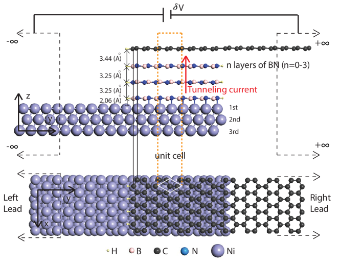
The model used in our study is shown in Fig. 1. Both the left lead (Ni) and the right lead (graphene) are assumed infinitely long. We also consider a case of Ni/(-BN)3/graphene with doubled overlapping area between Ni and BN as well as BN and graphene. We found a little change of the spin injection efficiency. Thus, we use the structure in Fig. 1 in this work. The scattering region or the device consists of the Ni lead at the bottom, the graphene active region at the top, and 0-3 layers of -BN (or Cu, graphene) between them. For convenience of discussion, we assume the transport direction is along the -direction and the normal direction of the graphene plane is the -direction. The system is periodic along the -direction, as shown in Fig. 1. It is noted that a single piece of graphene is used for the active region and the right lead which would minimize interface scattering between the central region and the right lead in the usual sandwich structures.
A separate slab model, consisting a monolayer graphene, 6 layers of Ni, and 0 to 3 layers of -BN was used for structural optimization and band structure calculation. During geometry optimization, the bottom four layers of Ni were fixed to their positions in bulk Ni while all other atoms in the system were allowed to freely relax. In the optimized structure, the distance between the graphene layer and the Ni substrate is 2.04 Å, while the BN-BN and BN-graphene interlayer distances are 3.25 Å and 3.44 Å, respectively (see Fig.1), which are in good agreement with results of previous theoretical studies.Avramov et al. (2012) The BN layer was found to interact strongly with Ni(111). In the optimized structure, the N atom in -BN sits on the top of the Ni atom in the surface layer, forming a N-Ni bond of length 2.06 Å. The B atom in -BN is directly above the Ni atom in the third layer, as shown in Fig. 1. The A-A stacking is assumed between BN and graphene because it is the most stable configuration among various possible stackings. The model for transport calculation was constructed from the optimized slab model.
III COMPUTATIONAL DETAILS
Geometry optimization and electronic structure calculation were carried out using the density functional theory (DFT) based VASP code.Kresse and Furthmüller (1996); Kresse and Furthmuller (1996) The projector augmented wave (PAW) method and the local density approximation (LDA)Perdew and Zunger (1981) were adopted to describe the core-valence interactions and the electron exchange and correlation functional. The plane-wave expansion of electron wavefunction was cutoff at a kinetic energy of 400 eV and the Brillouin zone of the unit cell was sampled using a 21211 -point grid. Structural optimization was carried out until the force on each atom is less than 0.01 eV/Å. The transport properties such as - curve were studied using a self-consistent approach that combines DFT and the non-equilibrium Green’s function (NEGF) formalism, as implemented in the ATK package,Brandbyge et al. (2002); Taylor et al. (2001) in which the electron transmission used in the Landauer’s formula is obtained self-consistently for a given value of bias voltage, same as in other previous works.Saha et al. (2012); Cho et al. (2011); Shen et al. (2012a, b); Bai et al. (2013) The double- polarized (DZP) basis set was used to expand the electron wave function in transport calculation and a cutoff energy of 150 Ry and a Monkhorst-Pack -point grid of yielded a good balance between accuracy and computational time. The LDA was also adopted in the transport calculations and the electron temperature was set to 300 K. A finer point mesh () was used to sample the periodic direction perpendicular to the transport direction. A vacuum region of 15 Å was used to separate the device from its periodic image to minimize the artificial interaction between them.
IV RESULTS AND DISCUSSIONS
IV.1 Transport property
IV.1.1 Ni(111)/graphene junction without tunnel barrier
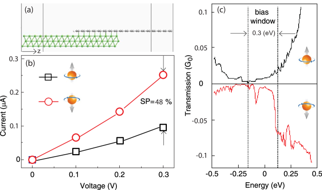
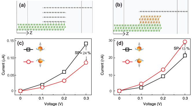
Before we examine the effect of a tunnel barrier, we calculate and present here the transport property of Ni(111)/graphene junction in which graphene is directly in contact with the Ni(111) electrode. The device structure is shown in Fig. 2a. It is similar to the structure shown in Fig. 1 but without the -BN layers. The calculated transmission spectrum of the Ni (111)/graphene junction under a bias voltage of 0.3 V is show in Fig. 2c where the bias voltage window is within the two vertical dashed lines. As can be seen, the total transmissions of spin up and spin down states are similar within the bias voltage window, except a peak near -0.10 eV in the spin down state. This implies that the spin polarization of the current passing through the device will not be high if the Ni lead is directly deposited on graphene.
For a more qualitative measure of spin polarization, i.e., spin injection efficiency from Ni lead into graphene, we calculate the - curves using the NEGF approach. The spin resolved current , where indicates the spin up or spin down state, is obtained from
| (1) |
where , , and are the electron charge, Planck’s constant, and the transmission, respectively. and in the above equation are the Fermi distribution functions of the left and right lead, respectively. Under a bias voltage , the chemical potentials of the left lead and right lead are shifted to and , respectively. The calculated - curve of the Ni(111)/graphene junction when the bias voltage is varied from 0 to 0.3 V is shown in Fig. 2b. It is clear that spin down electrons are the majority spin in the current. The spin down current is larger than the spin up current, but not overwhelmingly. This transport property can be partially explained by the electronic structure at the Fermi surface of Ni(111) and graphene.Karpan et al. (2007) When the Fermi surface of fcc Ni and graphene are projected to the (111) plane, higher density of states is found for down spin near the six high-symmetry points (K or K’) which are the main transport channels of graphene. In contrast, the Fermi surface states for up spin of Ni are located elsewhere.Karpan et al. (2007) Therefore, spin down electrons dominate over spin up electrons in the current under a bias voltage (Fig .2b). The spin injection efficiency is calculated from . Under a bias voltage of 0.3 V, the estimated spin injection efficiency of Ni(111)/graphene is 48%. This, however, is an optimistic value estimated based on an ideal model. Under experimental conditions, this value is expected to be reduced by interfacial effect such as interfacial disorder.Tombros et al. (2007); Popinciuc et al. (2009); Józsa et al. (2009a); Voloshina et al. (2011); Zhang et al. (2013, 2012)
IV.1.2 Ni(111)/graphene junction with -BN tunnel barrier
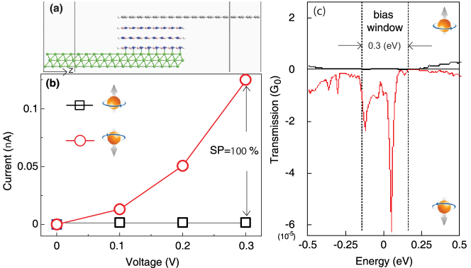
Spin tunneling has been proposed as a way of overcoming the conductance mismatch and has been widely used to enhance the spin injection efficiency of spintronic devices, such as silicon-based devices.Jansen (2012) It is therefore natural to ask whether the same approach works here and can be used to enhance spin injection efficiency from a FM lead to graphene. To investigate the effect of a tunnel barrier, we insert n () layers of -BN between Ni(111) and monolayer graphene, as illustrated in Fig. 1. The model used in our transport calculation is also shown in Fig. 3a. The spin tunneling transport properties of the Ni(111)/-BN/graphene were calculated and the results are presented in Fig. 3. As shown in Fig. 3c, the transmission spectrum of spin up states under a bias voltage of 0.3 V is greatly suppressed within the bias voltage window while that of the spin down states remains significant. The calculated - curve of the Ni(111)/-BN/graphene device with three layers of -BN (Fig. 3b) confirms that the majority spin current is much larger than the minority spin current under a bias voltage. The estimated spin injection efficiency of the Ni(111)/-BN/graphene device with 1-3 layers of -BN are given in Table 1. The results indicate that the spin injection efficiency from the ferromagnet into graphene can be dramatically enhanced by tunneling through an -BN barrier. With a single layer of -BN, the spin injection efficiency increased to 72%, which is close to the experimental results of 64% Yamaguchi et al. (2013), and much higher than 1% of FM/graphene Han et al. (2009) or 30% of FM/Oxide/graphene.Han et al. (2010) The maximum spin injection efficiency (100%) can be achieved with three or more layers of -BN between the FM lead and graphene. The enhancement of the spin injection efficiency is due to the improvement of conductance mismatch. Figure 2b and Figure 3b show the current () is reduced from A to A after inserting -BN. It means that the resistance of FM electrodes is increased by -BN barriers around 3 order of magnitude. Thus the resistance of RF and RG is close, indicating a good conductance match.
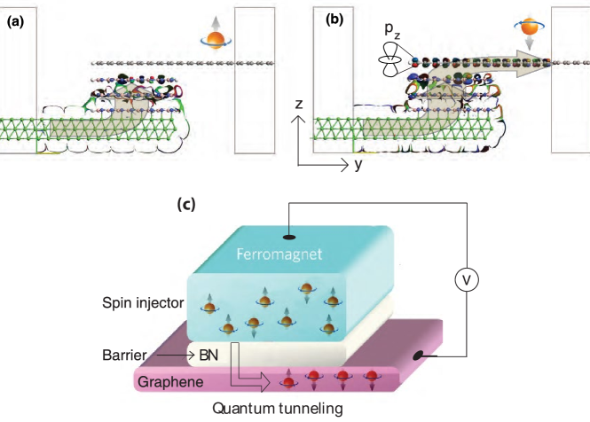
To understand how the -BN tunnel barrier affects the spin up and spin down currents, we calculated the spin-resolved transmission eigenstates and present the results for the device with three layers of -BN in Fig. 4. For the spin up states, we can see clearly in Fig. 4a that most of the transmission states are localized in the first two layers of -BN from the Ni electrode and a little on the N atoms in the third -BN layer which is next to graphene. The eigenstates in the third -BN layer show clear characteristics. Therefore, the transport channel of spin up states of graphene is essentially blocked. On the other hand, the spin down transmission states are delocalized in all -BN layers as well as graphene, as show in Fig. 4b. The transport channel of the spin down states of graphene is thus open, and the spin down electrons can be easily injected from the Ni electrode to graphene. It is noted that the transport channel in graphene is of carbon characteristic (Fig. 4b). Based on the spin-resolved transmission eigenstates of the two transport channels, we present a schematic diagram in Fig. 4c to illustrate the effect of the insulating barrier on the electron transport property of the proposed structure. Because of improved conductance matching by using a tunnel barrier,Han et al. (2010) spin polarized electric current is injected into graphene from a ferromagnetic electrode. The injected electric current is highly spin polarized because the majority spin transport channel is blocked by the tunnel barrier.
IV.1.3 Ni(111)/graphene junction with Cu or graphite barrier
Ni(111)/graphene/Ni(111) junction was proposed to have large magetoresistance (MR).Karpan et al. (2008, 2007); Saha et al. (2012); Giovannetti et al. (2008) The MR ratio (pessimistic) can reach 100% if five or more layers of graphene are used. But if a monolayer graphene is sandwiched between the open -shell transition-metals, such as Ni, its characteristic electronic structure of topological singularities at the -points in the reciprocal space would be destroyed by the formation of strong chemical bonds between graphene and transitional-metal electrodes, leading to a low MR ratio. Karpan et al., proposed to insert several layers of inert Cu to avoid bond formation between graphene and metal lead.Karpan et al. (2008) It was found that with a single layer of Cu between Ni and graphene, the electronic structure of graphene can be restored and its MR ratio can reach 90%. The MR ratio can be further increased by incorporating more layers of graphene between metal leads.Karpan et al. (2008)
Of course, magnetoresistance is different from spin injection ratio. The former relies on the magnetic configuration of the two electrodes, and is an extrinsic property of a system, while spin injection ratio is determined by the spin-dependent behaviors of injected electrons and it is an intrinsic property of the system. Despite of this difference, it is interesting to find out whether a Cu or graphite barrier is useful for enhancing the spin injection efficiency between graphene and the Ni(111) electrode. With this in mind and also to serve as a comparison with the -BN tunnel barrier, we also calculated the spin injection efficiencies of Ni(111)/graphene junctions with a few atomic layers of Cu (111) or graphite as barrier and list the results in Table 1. It is clear that the spin injection ratio is low with either graphite or Cu (111) as the barrier. The reason is because a few layers of graphite or Cu are metallic. The lack of tunneling effect makes the metallic barriers less effective in overcoming the conductance mismatch between Ni and graphene, compared to an insulating barrier such as -BN. Experimentally, it was demonstrated that a thin titanium seed layer between TM-electrodes and graphene improves the contact conductivity and lattice match, but does not lead to enhancement in spin injection ratio,Han et al. (2010) due to the same reason. Nevertheless, based on the results of our calculations, a good spin injection ratio (79%) may be achieved if a monolayer Cu (111) is inserted between the Ni (111) electrode and graphene. This is because the Cu layer weakens the interaction between Ni and graphene, allowing graphene to recover its characteristic electronic property. However, since Cu is metallic, electron transport through Cu is not by tunneling. If the thickness of the Cu barrier is more than one atomic layer, the spin injection ratio is hampered by the conductance mismatch between Cu and graphene. By comparing the performances of the three different barriers (Table 1), it is obvious that the insulating -BN, which interacts with graphene through the van der Waals force, is the most promising barrier to facilitate spin injection from a FM electrode into graphene, for graphene-based spintronic applications.
IV.2 Electronic structures
IV.2.1 Band structures
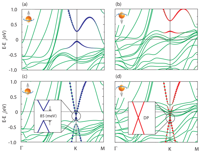
From the results of our transport calculations presented above, we know that the -BN tunnel barrier is effective in promoting spin injection from a TM-electrode into graphene. In order to understand the underlying physics, we calculated the spin-resolved band structure and local density of states of the Ni(111)/-BN/graphene structures. The results obtained for the structure with a single layer of -BN between Ni (111) and graphene are shown in Fig. 6, along with those without a -BN barrier for comparison. The solid circles in Fig. 6 represent the weight of the graphene-derived orbital. We pay attention to the graphene-derived orbital because it is the main transport channel as shown in Fig. 4b. As shown in Figs. 6a and 6b, when the Ni electrode is in direct contact with graphene, a band gap of about 0.34 eV opens in both spin up and spin down bands of graphene, which is in agreement with results of previous experiments and calculations.Karpan et al. (2008); Zhou et al. (2007); Giovannetti et al. (2007) The gap opening is due to strong interaction between graphene and Ni. The similar band structures for majority and minority carriers implies a low spin injection efficiency if the ferromagnetic Ni lead is directly deposit on graphene. In fact, because of the conductance mismatch between Ni and graphene ( ranges from to )Han et al. (2010), most of the charge carriers would be backscattered to Ni at the Ni/grpahene interface. Moreover, the measured spin polarization can be further reduced by interfacial effect and/or interfacial disorder in experimentally grown samples.Ke et al. (2008, 2010) All these result in a much lower spin injection efficiency into graphene.Tombros et al. (2007); Popinciuc et al. (2009); Józsa et al. (2009a) Interestingly, when a layer of -BN is incorporated between Ni and graphene, a band gap of about 85 meV opens in the spin up bands of graphene, while the spin down bands remain gap less, as shown in Figs. 6c and 6d. In other words, the semi-metallic characteristics of graphene is restored in the spin down states by the -BN layer. It is this -BN induced imbalance between the two spin states of graphene that results in the significantly different transport performance of the two spin channels. This is the root of the high spin injection efficiency of the Ni(111)/-BN/grpahene device.
IV.2.2 Local density of states
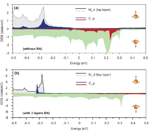
To understand why an -BN layer induces asymmetric effects on the two spin states of graphene, we examine the local density of states (LDOS) projected on the relevant atoms and orbitals. As can be seen in Fig. 7a, there exists a strong overlap between the C- and Ni- orbitals in both spin up states, in the energy range of -0.23 to -0.3 eV, and spin down states, between 0.23 and 0.28 eV, if metallic Ni is in direct contact with graphene. When one atomic layer of -BN is incorporated between Ni and graphene, the interaction between the C- and Ni- orbitals is eliminated in the spin down states, as shown in Fig. 7b. However, a weak coupling between these orbitals still exists in the spin up states, in the energy range of -0.3 to -0.32 eV. Further examination of the PDOS of other atoms reveals that this weak coupling is mediated by the N- orbitals (not shown here). These features in the PDOS of the concerned atoms and close relationship between DOS and transmission lend further support that Ni/-BN/graphene is an efficient tunneling barrier interface.
V CONCLUSIONS
The issue of spin conductance mismatch and resulting low spin injection efficiency which hampers the practical application of graphene in spintronics is addressed using first-principles electronic structure and transport calculations. -BN was found to be an effective tunnel barrier for enhancing the spin current injection efficiency from ferromagnetic electrodes into graphene. Our study suggests that tunneling transport can efficiently overcome the spin conductance mismatch between ferromagnetic electrodes and graphene, similar to other channel materials. Recently, Yamaguchi et al. demonstrated spin injection into bilayer graphene from ferromagnetic Ni0.8Fe0.2 electrodes through a single-crystal monolayer -BN.Yamaguchi et al. (2013) These studies pave the way for spintronic devices based on graphene as well as other 2D materials. Note that two-terminal devices should require more considerations besides the spin injection efficiency but will need to be treated along the guidelines in ref.7-9.
VI Acknowledgments
Authors thank S. C. Li, P. J. Kelly for their helpful comments on the discussion of Cu(111) and graphite barriers and asymmetric characteristics of two spin states of graphene with the -BN barrier. This work is partially supported by A*STAR (Singapore) Research Funding (Grant No. 092-156-0121).
References
- Geim and Novoselov (2007) A. K. Geim and K. S. Novoselov, The rise of graphene, Nat. Mater. 6, 183 (2007).
- Hill et al. (2006) E. W. Hill, A. K. Geim, K. Novoselov, F. Schedin, and P. Blake, Graphene spin valve devices, IEEE Trans. Mag. 42, 2694–2696 (2006).
- Han et al. (2009) W. Han, K. Pi, W. Bao, K. M. McCreary, Y. Li, W. H. Wang, C. N. Lau, and R. K. Kawakami, Electrical detection of spin precession in single layer graphene spin valves with transparent contacts, Appl. Phys. Lett. 94, 222109–222109 (2009).
- Tombros et al. (2007) N. Tombros, C. Jozsa, M. Popinciuc, H. T. Jonkman, and B. J. van Wees, Electronic spin transport and spin precession in single graphene layers at room temperature, Nature 448, 571 (2007).
- Popinciuc et al. (2009) M. Popinciuc, C. Jozsa, P. J. Zomer, N. Tombros, A. Veligura, H. T. Jonkman, and B. J. van Wees, Electronic spin transport in graphene field-effect transistors, Phys. Rev. B 80, 214427 (2009).
- Goto et al. (2008) H. Goto, A. Kanda, T. Sato, S. Tanaka, Y. Ootuka, S. Odaka, H. Miyazaki, K. Tsukagoshi, and Y. Aoyagi, Gate control of spin transport in multilayer graphene, Appl. Phys. Lett. 92, 212110 (2008).
- Schmidt et al. (2000) G. Schmidt, D. Ferrand, L. W. Molenkamp, A. T. Filip, and B. J. van Wees, Fundamental obstacle for electrical spin injection from a ferromagnetic metal into a diffusive semiconductor, Phys. Rev. B 62, R4790–R4793 (2000).
- Rashba (2000) E. I. Rashba, Theory of electrical spin injection: Tunnel contacts as a solution of the conductivity mismatch problem, Phys. Rev. B 62, R16267 (2000).
- Fert and Jaffres (2001) A. Fert and H. Jaffres, Conditions for efficient spin injection from a ferromagnetic metal into a semiconductor, Phys. Rev. B 64, 184420 (2001).
- Takahashi and Maekawa (2003) S. Takahashi and S. Maekawa, Spin injection and detection in magnetic nanostructures, Phys. Rev. B 67, 052409 (2003).
- Han et al. (2010) W. Han, K. Pi, K. M. McCreary, Y. Li, J. J. I. Wong, A. G. Swartz, and R. K. Kawakami, Tunneling spin injection into single layer graphene, Phys. Rev. Lett. 105, 167202 (2010).
- Dlubak et al. (2010) B. Dlubak, P. Seneor, A. Anane, C. Barraud, C. Deranlot, D. Deneuve, B. Servet, R. Mattana, F. Petroff, and A. Fert, Are Al2O3 and MgO tunnel barriers suitable for spin injection in graphene? Appl. Phys. Lett. 97, 092502 (2010).
- Józsa et al. (2008) C. Józsa, M. Popinciuc, N. Tombros, H. T. Jonkman, and B. J. Van Wees, Electronic spin drift in graphene field-effect transistors, Phys. Rev. Lett. 100, 236603 (2008).
- Józsa et al. (2009a) C. Józsa, M. Popinciuc, N. Tombros, H. T. Jonkman, and B. J. van Wees, Controlling the efficiency of spin injection into graphene by carrier drift, Phys. Rev. B 79, 081402 (2009a).
- Józsa et al. (2009b) C. Józsa, T. Maassen, M. Popinciuc, P. J. Zomer, A. Veligura, H. T. Jonkman, and B. J. van Wees, Linear scaling between momentum and spin scattering in graphene, Phys. Rev. B 80, 241403 (2009b).
- Dlubak et al. (2012) B. Dlubak, M.-B. Martin, C. Deranlot, K. Bouzehouane, S. Fusil, R. Mattana, F. Petroff, A. Anane, P. Seneor, and A. Fert, Homogeneous pinhole free 1 nm Al2O3 tunnel barriers on graphene, Appl. Phys. Lett. 101, 203104 (2012).
- Britnell et al. (2012a) L. Britnell, R. V. Gorbachev, R. Jalil, B. D. Belle, F. Schedin, A. Mishchenko, T. Georgiou, M. I. Katsnelson, L Eaves, S. V. Morozov, N. M. R. Peres, J. Leist, A. K. Geim, K. S. Novoselov, and L. A. Ponomarenko, Field-effect tunneling transistor based on vertical graphene heterostructures, Science 335, 947–950 (2012a).
- Roth et al. (2013) S. Roth, F. Matsui, T. Greber, and J. Osterwalder, Chemical vapor deposition and characterization of aligned and incommensurate graphene/hexagonal boron nitride heterostack on Cu (111), Nano. Lett. 13, 2668 (2013).
- Haigh et al. (2012) S. J. Haigh, A. Gholinia, R. Jalil, S. Romani, L. Britnell, D. C. Elias, K. S. Novoselov, L. A. Ponomarenko, A. K. Geim, and R. Gorbachev, Cross-sectional imaging of individual layers and buried interfaces of graphene-based heterostructures and superlattices, Nat. Mater. 11, 764 (2012).
- Kresse and Furthmüller (1996) G. Kresse and J. Furthmüller, Efficient iterative schemes for ab initio total-energy calculations using a plane-wave basis set, Phys. Rev. B 54, 11169 (1996).
- Kresse and Furthmuller (1996) G. Kresse and J. Furthmuller, Efficiency of ab-initio total energy calculations for metals and semiconductors using a plane-wave basis set, Com. Mater. Sci. 6, 15 (1996).
- Perdew and Zunger (1981) J. P. Perdew and A. Zunger, Self-interaction correction to density-functional approximations for many-electron systems, Phys. Rev. B 23, 5048 (1981).
- Brandbyge et al. (2002) M. Brandbyge, J.-L. Mozos, P. Ordejón, J. Taylor, and K. Stokbro, Density-functional method for nonequilibrium electron transport, Phys. Rev. B 65, 165401 (2002).
- Taylor et al. (2001) J. Taylor, H. Guo, and J. Wang, Ab initio modeling of quantum transport properties of molecular electronic devices, Phys. Rev. B 63, 245407 (2001).
- Saha et al. (2012) K. K. Saha, A. Blom, K. S. Thygesen, and B. K. Nikolić, Magnetoresistance and negative differential resistance in Ni/graphene/Ni vertical heterostructures driven by finite bias voltage: A first-principles study, Phys. Rev. B 85, 184426 (2012).
- Cho et al. (2011) Y. Cho, Y. C. Choi, and K. S. Kim, Graphene spin-valve device grown epitaxially on the Ni(111) substrate: A first principles study, J. Phys. Chem. C 115, 6019–6023 (2011).
- Shen et al. (2012a) L. Shen, M. Zeng, S. Li, M. B. Sullivan, and Y. P. Feng, Electron transmission modes in electrically biased graphene nanoribbons and their effects on device performance, Phys. Rev. B 86, 115419 (2012a).
- Shen et al. (2012b) L. Shen, T. Zhou, Z. Bai, J. Q. Zeng, M.and Goh, Z.-M. Yuan, G. Han, B. Liu, and Y. P. Feng, Systematic study of ferroelectric, interfacial, oxidative, and doping effects on conductance of Pt/BaTiO3/Pt ferroelectic tunnel junctions, Phys. Rev. B 85, 064105 (2012b).
- Bai et al. (2013) Z. Bai, L. Shen, Q. Wu, M. Zeng, J.-S. Wang, G. Han, and Y. P. Feng, Boron diffusion induced symmetry reduction and scattering in CoFeB/MgO/CoFeB magnetic tunnel junctions, Phys. Rev. B 87, 014114 (2013).
- Britnell et al. (2012b) L. Britnell, R. V. Gorbachev, R. Jalil, B. D. Belle, F. Schedin, M. I. Katsnelson, L. Eaves, S. V. Morozov, A. S. Mayorov, N. M. R. Peres, A. H. Castro Neto, J. Leist, A. K. Geim, L. A. Ponomarenko, and K. S. Novoselov, Electron tunneling through ultrathin boron nitride crystalline barriers, Nano. Lett. 12, 1707–1710 (2012b).
- Georgiou et al. (2013) T. Georgiou, R. Jalil, B. D. Belle, L. Britnell, R. V. Gorbachev, S. V. Morozov, Y.-J. Kim, A. Gholinia, S. J. Haigh, O. Makarovsky, L. Eaves, L. A. Ponomarenko, A. K. Geim, K. S. Novoselov, and A. Mishchenko, Vertical field-effect transistor based on graphene-WS2 heterostructures for flexible and transparent electronics, Nat. Nanotech. 8, 100–103 (2013).
- Choi et al. (2013) M. S. Choi, G.-H. Lee, Y.-J. Yu, D.-Y. Lee, S. H. Lee, P. Kim, J. Hone, and W. J. Yoo, Controlled charge trapping by molybdenum disulphide and graphene in ultrathin heterostructured memory devices, Nat. Commun. 4, 1624 (2013).
- Yu et al. (2012) W. J. Yu, Z. Li, H. Zhou, Y. Chen, Y. Wang, Y. Huang, and X. Duan, Vertically stacked multi-heterostructures of layered materials for logic transistors and complementary inverters, Nat. Mater. 12, 246 (2012).
- Geim and Grigorieva (2013) A. K. Geim and I. V. Grigorieva, Van der Waals heterostructures, Nature 499, 419 (2013).
- Liu et al. (2012) H. Liu, H. Kondo, and T. Ohno, Contact effects of nickel and copper on electron transport through graphene, Phys. Rev. B 86, 155434 (2012).
- Maassen et al. (2011) J. Maassen, W. Ji, and H. Guo, Graphene spintronics: The role of ferromagnetic electrodes, Nano. Lett. 11, 151–155 (2011).
- Karpan et al. (2008) V. M. Karpan, P. A. Khomyakov, A. A. Starikov, G. Giovannetti, M. Zwierzycki, M. Talanana, G. Brocks, J. Van Den Brink, and P. J. Kelly, Theoretical prediction of perfect spin filtering at interfaces between close-packed surfaces of Ni or Co and graphite or graphene, Phys. Rev. B 78, 195419 (2008).
- Karpan et al. (2007) V. M. Karpan, G. Giovannetti, P. A. Khomyakov, M. Talanana, A. A. Starikov, M. Zwierzycki, J. Van Den Brink, G. Brocks, and P. J. Kelly, Graphite and graphene as perfect spin filters, Phys. Rev. Lett. 99, 176602 (2007).
- Yazyev and Pasquarello (2009) O. V. Yazyev and A. Pasquarello, Magnetoresistive junctions based on epitaxial graphene and hexagonal boron nitride, Phys. Rev. B 80, 035408 (2009).
- Karpan et al. (2011) V. M. Karpan, P. A. Khomyakov, G. Giovannetti, A. A. Starikov, and P. J. Kelly, Ni(111)graphene-BN junctions as ideal spin injectors, Phys. Rev. B 84, 153406 (2011).
- Giovannetti et al. (2007) G. Giovannetti, P. A. Khomyakov, G. Brocks, P. J. Kelly, and J. van den Brink, Substrate-induced band gap in graphene on hexagonal boron nitride: Ab initio density functional calculations, Phys. Rev. B 76, 073103 (2007).
- Avramov et al. (2012) P. V. Avramov, A. A. Kuzubov, S. Sakai, M. Ohtomo, S. Entani, Y. Matsumoto, H. Naramoto, and N. S. Eleseeva, Contact-induced spin polarization in graphene/h-BN/Ni nanocomposites, J. Appl. Phys. 112, 114303–114303 (2012).
- Voloshina et al. (2011) E. N. Voloshina, A. Generalov, M. Weser, S. Böttcher, K. Horn, and Y. S. Dedkov, Structural and electronic properties of the graphene/Al/Ni (111) intercalation system, New J. Phys. 13, 113028 (2011).
- Zhang et al. (2013) C. Zhang, Y. Wang, B. Wu, and Y. Wu, The effect of a copper interfacial layer on spin injection from ferromagnet to graphene, Appl. Phys. A 111, 339–345 (2013).
- Zhang et al. (2012) C. Zhang, Y. Wang, B. Wu, and Y. Wu, Enhancement of spin injection from ferromagnet to graphene with a Cu interfacial layer, Appl. Phys. Lett. 101, 022406 (2012).
- Jansen (2012) R. Jansen, Silicon spintronics, Nat. Mater. 11, 400–408 (2012).
- Giovannetti et al. (2008) G. Giovannetti, P. A. Khomyakov, G. Brocks, V. M. Karpan, J. Van den Brink, and P. J. Kelly, Doping graphene with metal contacts, Phys. Rev. Lett. 101, 026803 (2008).
- Ke et al. (2008) Y. Ke, K. Xia, and H. Guo, Disorder scattering in magnetic tunnel junctions: theory of nonequilibrium vertex correction, Phys. Rev. Lett. 100, 166805 (2008).
- Ke et al. (2010) Y. Ke, K. Xia, and H. Guo, Oxygen vacancy-induced diffusion scattering, Phys. Rev. Lett. 105, 236801 (2010).
- Zhou et al. (2007) S. Y. Zhou, G.-H. Gweon, A. V. Fedorov, P. N. First, W. A. De Heer, D.-H. Lee, F. Guinea, A. H. Castro Neto, and A. Lanzara, Substrate-induced bandgap opening in epitaxial graphene, Nat. Mater. 6, 770–775 (2007).
- Yamaguchi et al. (2013) T. Yamaguchi, Y. Inoue, S. Masubuchi, S. Morikawa, M. Onuki, K. Watanabe, T. Taniguchi, R. Moriya, and T. Machida, Electrical spin injection into graphene through monolayer hexagonal boron nitride, arXiv:1305.7095 (2013).
| Barrier | Spin injection efficiency | ||
|---|---|---|---|
| 1L | 2L | 3L | |
| -BN | 72% | 96% | 100% |
| Graphene | 29% | 31% | 24% |
| Cu (111) | 79% | 12% | 13% |