See pages 1-last of 14q1118.pdf
Supplemental Material
Synthesized multiwall MoS2 nanotube and nanoribbon field-effect transistors
S. Fathipour 1, M. Remskar 2, A. Varlec 2, A. Ajoy 1,a, R. Yan 3, S. Vishwanath 1, W. S. Hwang 4,
H. G. Xing 1, D. Jena 1,b, and A. Seabaugh 1
1 Department of Electrical Engineering, University of Notre Dame, Notre Dame, Indiana 46556, USA
2 Solid State Physics Department, Jožef Stefan Institute, Ljubljana, Slovenia
3 Department of Electrical Engineering, Cornell University, Ithaca, New York 14850, USA
4 Department of Materials Engineering, Korea Aerospace University, Gyeonggi 412791, Korea
a) aajoy@nd.edu
b) djena@nd.edu
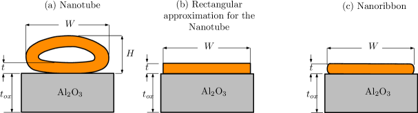
In this supplemental material, we attempt to model the current-voltage characteristics of the MoS2 nanotube (NT) and nanoribbon (NR) MOSFETs. The growth of the NTs and NRs results in the MoS2 being unintentionally -doped. The fabricated -type MOSFETs are hence accumulation-depletion devices – the channel is accumulated when the device is in the on-state, and is depleted of carriers as the device turns off. In accumulation, the channel is dominated by electrons that are close to the oxide-semiconductor interface. As the device turns off, the channel is dominated by electrons that are farther away from this interface. We restrict ourselves to gate voltages for which the channel is accumulated. In this regime, it is hence reasonable to approximate the cross section of the NT MOSFETs by a rectangle, as shown in Fig. S1. The thickness of this rectangle corresponds to the thickness of the wall of the NT. This approximation allows us to apply results derived for an -type junctionless FET [1] to model both the NT and NR MOSFETs.
1 Model
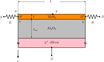
See Fig. S2. , and refer to the external terminals of the MOSFET. Source and drain contact resistances (assumed equal, ) connect , to intrinsic nodes and respectively. When a current flows through the device, the terminal and intrinsic voltages are given by , . Within the intrinsic MOSFET, the electron concentration is , where is the quasi-Fermi potential, is the electrostatic potential [2, 3], is the unintentional doping concentration, and is the thermal voltage. The surface potential at the oxide-semiconductor interface is obtained by a solution of the following implicit equation
| (S1) |
where is the flat-band voltage, is the dielectric constant of MoS2 and with , being the dielectric constant and thickness of the Al2O3 respectively. Note that this equation has been derived under the condition that the net charge density at the rear interface () is zero in accumulation (which corresponds to ). Setting and in eq. (S1) respectively yields the surface potentials and (corresponding to the points shown in Fig. S2). The current is then
| (S2) | ||||
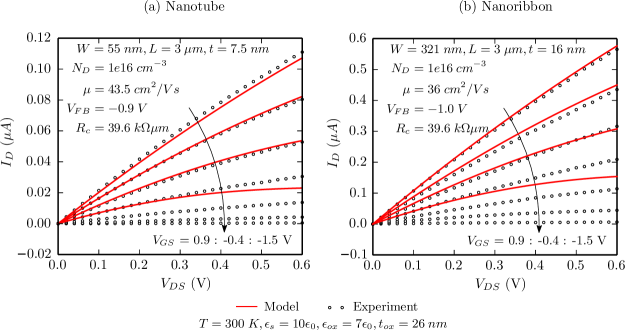
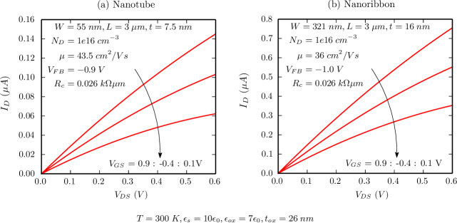
where is an effective value of mobility, and . A comparison of the experimental data with the results of the above model is shown in Fig. S3.
2 Verification of zero charge density approximation
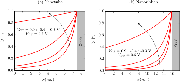
We verify whether the approximation of zero net charge density at is valid for the - curves we have modeled. To do this, we solve the electrostatic problem without this approximation, in terms of the surface potential and surface electric field obtained using the zero charge density approximation. This allows us to plot the charge density as a function of . Our approximation is reasonable if so obtained is close to zero. We begin with Poisson’s equation under the gradual channel approximation given by
| (S3) |
Integrating eq. (S3) by parts, we get (where the electric field ), which yields
| (S4) |
The negative sign for the square root is sensible in the accumulation regime. Eq. (S4) can be cast as an ordinary differential equation , with , and can be solved numerically to obtain and , given the values of (which were obtained from a solution of eq. (S1) ). The results from this calculation are shown in Fig. S4. The value of in eq. (S4) is chosen to be equal to . Notice that the approximation is the best for the largest value of , and worst for the lowest value of . This corresponds to the trends seen in Fig. S3.
3 Projection assuming ideal contacts
The minimum contact resistance to a 2-D material is given by , where is the sheet charge density in units of [5]. Assuming that in the above expression, the minimum contact resistance is . Note that the value of contact resistance measured in our NT MOSFET is . Fig. S5 predicts the currents that can be obtained from our NT and NR MOSFETs, provided the contact resistance is chosen to be . Improving the contacts in this manner causes a ( ) increase in the currents of the NT (NR) at .
4 Conclusion
In conclusion, we have modeled the characteristics of the fabricated NT and NR MOSFETs operating in a regime where the entire channel is accumulated. The results of this model compare well with the experimental data. We extract effective mobilities of and for the NT and NR MOSFETs respectively.
References
- [1] Z. Chen, Y. Xiao, M. Tang, Y. Xiong, J. Huang, J. Li, X. Gu, and Y. Zhou, “Surface-potential-based drain current model for long-channel junctionless double-gate mosfets,” IEEE Trans. Electron Devices, vol. 59, no. 12, pp. 3292–3298, 2012.
- [2] H. C. Pao and C.-T. Sah, “Effects of diffusion current on characteristics of metal-oxide (insulator)-semiconductor transistors,” Solid State Electron., vol. 9, no. 10, pp. 927–937, 1966.
- [3] A. Ortiz-Conde, R. Herrera, P. Schmidt, F. Sánchez, and J. Andrian, “Long-channel silicon-on-insulator MOSFET theory,” Solid State Electron., vol. 35, no. 9, pp. 1291–1298, 1992.
- [4] S. Kim, A. Konar, W.-S. Hwang, J. H. Lee, J. Lee, J. Yang, C. Jung, H. Kim, J.-B. Yoo, J.-Y. Choi et al., “High-mobility and low-power thin-film transistors based on multilayer MoS2 crystals,” Nature Communications, vol. 3, p. 1011, 2012.
- [5] D. Jena, K. B. Banerjee, and G. H. Xing, “Intimate contacts,” (to appear) Nature Materials.