Mexican Hat and Rashba Bands in Few-Layer van der Waals Materials
Abstract
The valence band of a variety of few-layer, two-dimensional materials consists of a ring of states in the Brillouin zone. The energy-momentum relation has the form of a ‘Mexican hat’ or a Rashba dispersion. The two-dimensional density of states is singular at or near the band edge, and the band-edge density of modes turns on nearly abruptly as a step function. The large band-edge density of modes enhances the Seebeck coefficient, the power factor, and the thermoelectric figure of merit ZT. Electronic and thermoelectric properties are determined from ab initio calculations for few-layer III-VI materials GaS, GaSe, InS, InSe, for Bi2Se3, for monolayer Bi, and for bilayer graphene as a function of vertical field. The effect of interlayer coupling on these properties in few-layer III-VI materials and Bi2Se3 is described. Analytical models provide insight into the layer dependent trends that are relatively consistent for all of these few-layer materials. Vertically biased bilayer graphene could serve as an experimental test-bed for measuring these effects.
I Introduction
The electronic bandstructure of many two-dimensional (2D), van der Waals (vdW) materials qualitatively changes as the thickness is reduced down to a few monolayers. One well known example is the indirect to direct gap transition that occurs at monolayer thicknesses of the Mo and W transition metal dichalcogenides (TMDCs)Mak et al. (2010). Another qualitative change that occurs in a number of 2D materials is the inversion of the parabolic dispersion at a band extremum into a ‘Mexican hat’ dispersion.Stauber et al. (2007); Zolyomi et al. (2013, 2014) Mexican hat dispersions are also referred to as a Lifshiftz transition Zhang et al. (2010); Zolyomi et al. (2013); Varlet et al. (2014), an electronic topological transition Blanter et al. (1994) or a camel-back dispersion Wang et al. (2014); Peng et al. (2014). In a Mexican hat dispersion, the Fermi surface near the band-edge is approximately a ring in -space, and the radius of the ring can be large, on the order of half of the Brillouin zone. The large degeneracy coincides with a singularity in the two-dimensional (2D) density of states close to the band edge. A similar feature occurs in monolayer Bi due to the Rashba splitting of the valence band. This also results in a valence band edge that is a ring in -space although the diameter of the ring is generally smaller than that of the Mexican hat dispersion.
Mexican hat dispersions are relatively common in few-layer two-dimensional materials. Ab-initio studies have found Mexican hat dispersions in the valence band of many few-layer III-VI materials such as GaSe, GaS, InSe, InS Zolyomi et al. (2013, 2014); Hu et al. (2013); Zhuang and Hennig (2013); Cao et al. (2014); Wu et al. (2014). Experimental studies have demonstrated synthesis of monolayers and or few layers of GaS, GaSe and InSe thin films.Lei et al. (2013, 2014); Hu et al. (2013, 2012); Late et al. (2012); Li et al. (2014); Mahjouri-Samani et al. (2014); Shen et al. (2009). Monolayers of Bi2Te3 Zahid and Lake (2010), and Bi2Se3 Saeed et al. (2014) also exhibit a Mexican hat dispersion in the valence band. The conduction and valence bands of bilayer graphene distort into approximate Mexican hat dispersions, with considerable anisotropy, when a a vertical field is applied across AB-stacked bilayer graphene. Min et al. (2007); Stauber et al. (2007); Varlet et al. (2014) The valence band of monolayer Bi(111) has a Rashba dispersion. Takayama et al. (2011)
The large density of states of the Mexican hat dispersion can lead to instabilities near the Fermi level, and two different ab initio studies have recently predicted Fermi-level controlled magnetism in monolayer GaSe and GaS Cao et al. (2014); Wu et al. (2014). The singularity in the density of states and the large number of conducting modes at the band edge can enhance the Seebeck coefficient, power factor, and the thermoelectric figure of merit ZT. Mahan and Sofo (1996); Heremans et al. (2008, 2012) Prior studies have achieved this enhancement in the density of states by using nanowires Hicks and Dresselhaus (1993); Dresselhaus et al. (2007), introducing resonant doping levels Heremans et al. (2008, 2012), high band degeneracy Pei et al. (2011); Sootsman et al. (2009), and using the Kondo resonance associated with the presence of localized and orbitals Fuccillo et al. (2013); Sun et al. (2009); Zhang et al. (2011). The large increase in ZT predicted for monolayer Bi2Te3 resulted from the formation of a Mexican hat bandstructure and its large band-edge degeneracy Zahid and Lake (2010); Maassen and Lundstrom (2013).
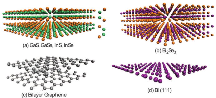
This work theoretically investigates the electronic and thermoelectric properties of a variety of van der Waals materials that exhibit a Mexican hat dispersion or Rashba dispersion. The Mexican hat and Rashba dispersions are first analyzed using an analytical model. Then, density functional theory is used to calculate the electronic and thermoelectric properties of bulk and one to four monolayers of GaX, InX (X = Se, S), Bi2Se3, monolayer Bi(111), and bilayer graphene as a function of vertical electric field. Figure 1 illustrates the investigated structures that have either a Mexican hat or Rashba dispersion.
The analytical model combined with the numerically calculated orbital compositions of the conduction and valence bands explain the layer dependent trends that are relatively consistent for all of the few-layer materials. While numerical values are provided for various thermoelectric metrics, the emphasis is on the layer-dependent trends and the analysis of how the bandstructure affects both the electronic and thermoelectric properties. The metrics are provided in such a way that new estimates can be readily obtained given new values for the electrical or thermal conductivity.
II Models and Methods
II.1 Landauer Thermoelectric Parameters
In the linear response regime, the electronic and thermoelectric parameters are calculated within a Landauer formalism. The basic equations have been described previously Maassen and Lundstrom (2013); Paul et al. (2012); Wickramaratne et al. (2014), and we list them below for convenience. The equations for the electronic conductivity (), the electronic thermal conductivity (), and the Seebeck coefficient (S) are
| (1) | ||||
| (2) | ||||
| (3) | ||||
| (4) | ||||
where is the device length, is the dimensionality (1, 2, or 3), is the magnitude of the electron charge, is Planck’s constant, is Boltzmann’s constant, and is the Fermi-Dirac factor. The transmission function is
| (5) |
where M(E) as the density of modes. In the diffusive limit,
| (6) |
where is the electron mean free path. The power factor () and the thermoelectric figure of merit () are given by and
| (7) |
where is the lattice thermal conductivity.
II.2 Analytical Models
The single-spin density of modes for transport in the direction is Datta (2005); Jeong et al. (2010)
| (8) |
where is the dimensionality, is the energy, and is the band dispersion. The sum is over all values of such that , i.e. all momenta with positive velocities. The dimensions are , so that in 2D, gives the number of modes per unit width at energy . If the dispersion is only a function of the magnitude of , then Eq. (8) reduces to
| (9) |
where for , for , and for . is the magnitude of such that , and the sum is over all bands and all values of within a band. When a band-edge is a ring in -space with radius , the single-spin 2D density of modes at the band edge is
| (10) |
where is either 1 or 2 depending on the type of dispersion, Rashba or Mexican hat. Thus, the 2D density of modes at the band edge depends only on the radius of of the -space ring. For a two dimensional parabolic dispersion, , the radius is 0, and Eq. (9) gives a the single-spin density of modes of Kim et al. (2009)
| (11) |
In real III-VI materials, there is anisotropy in the Fermi surfaces, and a 6th order, angular dependent polynomial expression is provided by Zólyomi et al. that captures the low-energy anisotropy Zolyomi et al. (2013, 2014). To obtain physical insight with closed form expressions, we consider a 4th order analytical form for an isotropic Mexican hat dispersion
| (12) |
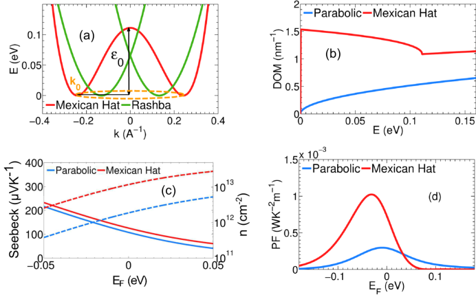
where is the height of the hat at , and is the magnitude of the effective mass at . A similar quartic form was previously used to analyze the effect of electron-electron interactions in biased bilayer graphene Stauber et al. (2007). The function is plotted in Figure 2(a).
The band edge occurs at , and, in -space, in two dimensions (2D), it forms a ring in the plane with a radius of
| (13) |
For the two-dimensional Mexican hat dispersion of Eq. (12), the single-spin density of modes is
| (14) |
Figure 2(b) shows the density of mode distributions plotted from Eqs. (11) and (14). At the band edge (), the single-spin density of modes of the Mexican hat dispersion is finite,
| (15) |
The Mexican hat density of modes decreases by a factor of as the energy increases from 0 to , and then it slowly increases. The step-function turn-on of the density of modes is associated with a singularity in the density of states. The single-spin density of states resulting from the Mexican hat dispersion is
| (16) |
Rashba splitting of the spins also results in a valence band edge that is a ring in -space. The Bychkov-Rashba model with linear and quadratic terms in gives an analytical expression for a Rashba-split dispersion, Bychkov and Rashba (1984)
| (17) |
where the Rashba parameter, , is the strength of the Rashba splitting. In Eq. (17), the bands are shifted up by so that the band edge occurs at . The radius of the band edge in -space is
| (18) |
The energy dispersion of the split bands is illustrated in Figure 2(a). The density of modes, including both spins, resulting from the dispersion of Eq. (17) is
| (19) |
For , the density of modes is a step function and the height is determined by and the effective mass. Values for vary from 0.07 eVÅ in InGaAs/InAlAs quantum wells to 0.5 eVÅ in the Bi(111) monolayer.Ishizaka et al. (2011) The density of states including both spins is
| (20) |
In general, we find that the diameter of the Rashba -space rings are less than the diameter of the Mexican hat -space rings, so that the enhacements to the thermoelectric parameters are less from Rashba-split bands than from the inverted Mexican hat bands.
In the real bandstructures considered in the Sec. IV, there is anisotropy to the -space Fermi surfaces. The band extrema at K and M have different energies. For the III-VIs, Bi2Se3, and monolayer Bi, this energy difference is less than at room temperature. In the III-VIs, the maximum energy difference between the valence band extrema at K and M is 6.6 meV in InS. In Bi2Se3, it is 19.2 meV, and in monolayer Bi, it is 0.5 meV. The largest anisotropy occurs in bilayer graphene under bias. At the maximum electric field considered of 0.5 V/Å, the energy difference of the extrema in the conduction band is 112 meV, and the energy difference of the extrema in the valence band is 69 meV. The anisotropy experimentally manifests itself in the quantum Hall plateaus.Varlet et al. (2014) Anisotropy results in a finite slope to the turn-on of the density of modes and a shift of the singularity in the density of states away from the band edge. The energy of the singularity in the density of states lies between the two extrema Zolyomi et al. (2013, 2014).
Figure 2(c) compares the Seebeck coefficients and the electron densities calculated from the Mexican hat dispersion shown in Fig. 2(a) and a parabolic dispersion. The quantities are plotted versus Fermi energy with the conduction band edge at . The bare electron mass is used for both dispersions, , and, for the Mexican hat, eV which is the largest value for obtained from our ab-initio simulations of the III-VI compounds. The temperature is K. The Seebeck coefficients are calculated from Eqs. (3), (4), and (5) with . The electron densities are calculated from the density of state functions given by two times Eq. (16) for the Mexican hat dispersion and by for the parabolic dispersion. Over the range of Fermi energies shown, the electron density of the Mexican hat dispersion is approximately 6 times larger than that of the parabolic dispersion. To gain further insight, consider the itegrals of the density of states for low energies near the band edges, . For the parabolic dispersion, , and for the Mexican hat dispersion, . The ratio is . One factor of 2 results from the two branches of the Mexican hat dispersion at low energies () and a second factor of 2 results from integrating . In this case, eV, so that at eV, gives a factor of 1.5 resulting in a total factor of 6 in the ratio which is consistent with the numerical calculation at finite temperature shown in Fig. 2(c). There are two important points to take away from this plot. At the same electron density, the Fermi level of the Mexican hat dispersion is much lower than that of the parabolic dispersion. At the same electron density, the Seebeck coefficient of the Mexican dispersion is much larger than the Seebeck coefficient of the parabolic dispersion.
Figure 2(d) compares the ballistic power factors calculated from the Mexican hat dispersion shown in Fig. 2(a) and the parabolic dispersion, again with for both dispersions. The temperature is K. The ballistic power factor is calculated from Eqs. (1), (3), (4), and (5) with . Eqs. (11) and (14) for the density of modes are used in Eq. (5). The peak power factor of the Mexican hat dispersion occurs when meV, i.e. 30 meV below the conduction band edge. This is identical to the analytical result obtained by approximating the density of modes as an ideal step function. The peak power factor of the parabolic dispersion occurs when meV. At the peak power factors, the value of of the Mexican hat dispersion is 3.5 times larger than of the parabolic dispersion, and of the Mexican hat dispersion is 3.2 times larger than of the parabolic dispersion. The reason for the larger increase in compared to is that, at the maximum power factor, the Fermi level of the Mexican hat dispersion is further below the band edge. Thus, the factor in the integrand of increases, and the average energy current referenced to the Fermi energy given by increases more than the average particle current given by . Since the ratio gives the Seebeck coefficient, this translates into an increase of the Seebeck coefficient at the peak power factor. At the peak power factors, the Seebeck coefficient of the Mexican hat dispersion is enhanced by 10 compared to the parabolic dispersion. We consistently observe a larger increase in compared to that of at the peak power factor when comparing monolayer structures with Mexican hat dispersions to bulk structures with parabolic dispersions. For the III-VI materials, at their peak power factors, GaSe shows a maximum increase of the Seebeck coefficient of 1.4 between a monolayer with a Mexican hat dispersion and bulk with a parabolic dispersion. The power factor is proportional to . Since the increase in at the peak power factor lies between 1 and 1.4, the large increase in the maximum power factor results from the large increase in . Since the increase in is within a factor of 1 to 1.4 times the increase in , one can also view the increase in the power factor as resulting from an increase in which is simply the particle current or conductivity. The increase of both of these quantities, or , results from the increase in the density of modes near the band edge available to carry the current. Over the range of integration of several of the band edge, the density of modes of the Mexican hat dispersion is significantly larger than the density of modes of the parabolic dispersion as shown in Fig. 2(c).
From the Landauer-Büttiker perspective of Eq. (5), the increased conductivity results from the increased number of modes. From a more traditional perspective, the increased conductivity results from an increased density of states resulting in an increased charge density . At their peak power factors, the charge density of the Mexican hat dispersion is cm-2, and the charge density of the parabolic dispersion is cm-2. The charge density of the Mexican hat dispersion is 3.2 times larger than the charge density of the parabolic dispersion even though the Fermi level for the Mexican hat dispersion is 22.5 meV less than the Fermi level of the parabolic dispersion. Since the peak power factor always occurs when is below the band edge, the charge density resulting from the Mexican hat dispersion will always be significantly larger than that of the parabolic dispersion. This, in general, will result in a higher conductivity.
When the height of the Mexican hat is reduced by a factor of 4 ( is reduced by a factor of 2), the peak power factor decreases by a factor of 2.5, the Fermi level at the peak power factor increases from -30 meV to -20.1 meV, and the corresponding electron density decreases by a factor 2.3. When is varied with respect to the thermal energy at 300K using the following values, 5kBT, 2kBT, kBT and 0.5kBT the ratios of the Mexican hat power factors with respect to the parabolic band power factors are 3.9, 2.2, 1.5 and 1.1, respectively. The above analytical discussion illustrates the basic concepts and trends, and it motivates the following numerical investigation of various van der Waals materials exhibiting either Mexican hat or Rashba dispersions.
III Computational Methods
Ab-initio calculations of the bulk and few-layer structures (one to four layers) of GaS, GaSe, InS, InSe, Bi2Se3, Bi(111) surface, and bilayer graphene are carried out using density functional theory (DFT) with a projector augmented wave method Blöchl (1994) and the Perdew-Burke-Ernzerhof (PBE) type generalized gradient approximation Perdew et al. (1996); Ernzerhof and Scuseria (1999) as implemented in the Vienna ab-initio Simulation Package (VASP). Kresse and Hafner (1993); Kresse and Furthmuller (1996) The vdW interactions in GaS, GaSe, InS, InSe and Bi2Se3 are accounted for using a semi-empirical correction to the Kohn-Sham energies when optimizing the bulk structures of each material.Grimme (2006) For the GaX, InX (X = S,Se), Bi(111) monolayer, and Bi2Se3 structures, a Monkhorst-Pack scheme is used for the integration of the Brillouin zone with a k-mesh of 12 x 12 x 6 for the bulk structures and 12 x 12 x 1 for the thin-films. The energy cutoff of the plane wave basis is 300 eV. The electronic bandstructure calculations include spin-orbit coupling (SOC) for the GaX, InX, Bi(111) and Bi2Se3 compounds. To verify the results of the PBE band structure calculations of the GaX and InX compounds, the electronic structures of one to four monolayers of GaS and InSe are calculated using the Heyd-Scuseria-Ernzerhof (HSE) functional.Heyd et al. (2003) The HSE calculations incorporate 25 short-range Hartree-Fock exchange. The screening parameter is set to 0.2 Å-1. For the calculations on bilayer graphene, a 32 32 1 k-point grid is used for the integration over the Brillouin zone. The energy cutoff of the plane wave basis is 400 eV. 15Å of vacuum spacing was added to the slab geometries of all few-layer structures.
The ab-initio calculations of the electronic structure are used as input into a Landauer formalism for calculating the thermoelectric parameters. The two quantities requred are the density of states and the density of modes. The density of states is directly provided by VASP. The density of modes calculations are performed by integrating over the first Brillouin zone using a converged k-point grid, k-points for the bulk structures and k-points for the III-VI, Bi2Se3 and Bi(111) thin film structures. A grid of k-points is required for the density of mode calculations on bilayer graphene. The details of the formalism are provided in several prior studies.Maassen and Lundstrom (2013); Paul et al. (2012); Wickramaratne et al. (2014) The temperature dependent carrier concentrations for each material and thickness are calculated from the density-of-states obtained from the ab-initio simulations. To obtain a converged density-of-states a minimum k-point grid of 727236 (72721) is required for the bulk (monolayer and few-layer) III-VI and Bi2Se3 structures. For the density-of-states calculations on bilayer graphene and monolayer Bi(111) a 36361 grid of k-points is used.
The calculation of the conductivity, the power factor, and requires values for the electron and hole mean free paths and the lattice thermal conductivity. Electron and hole scattering are included using a constant mean free path, determined by fitting to experimental data. For GaS, GaSe, InS and InSe, = 25 nm gives the best agreement with experimental data. Ismailov et al. (1966); Micocci et al. (1990); Krishna and Reddy (1983); Mane and Lokhande (2003) The room temperature bulk n-type electrical conductivity of GaS, GaSe, InS and InSe at room temperature was reported to be 0.5 m-1, 0.4 m-1, 0.052 m-1 and 0.066 m-1 respectively at a carrier concentration of 1016 cm-3. Using = 25 nm for bulk GaS, GaSe and InSe we obtain an electrical conductivity of 0.58 m-1, 0.42 m-1, 0.058 m-1 and 0.071 m-1, respectively at the same carrier concentration. For the Bi(111) monolayer surface, the relaxation time for scattering in bulk Bi is reported to be 0.148 ps at 300K.Cheng et al. (2013) Using the group velocity of the conduction and valence bands ( m/sec for electrons and holes) from our ab-initio simulations, an electron and hole mean free path of 10 nm is used to determine the thermoelectric parameters of the Bi(111) monolayer. Prior theoretical studies of scattering in thin films of Bi2Se3 ranging from 2 QLs to 4 QLs give a scattering time on the order of 10 fs.Yin et al. (2013a, 2014); Saeed et al. (2014) Using a scattering time of = 10 fs and electron and hole group velocities from the ab-initio simulations of 3 105 m/s and 2.4105 m/s, respectively, electron and hole mean free paths of =3 nm and =2.4 nm are used to extract the thermoelectric parameters for bulk and thin film Bi2Se3. For bilayer graphene, = 88 nm gives the best agreement with experimental data on conductivity at room temperature.Wang et al. (2011)
Values for the lattice thermal conductivity are also taken from available experimental data. The thermal conductivity in defect-free thin films is limited by boundary scattering and can be up to an order of magnitude lower than the bulk thermal conductivity.Jeong et al. (2012) As the thickness of the film increases, approaches the Umklapp limited thermal conductivity of the bulk structure. Hence, the values of obtained from experimental studies of bulk materials for this study are an upper bound approximation of in the thin film structures. The experimental value of 10 Wm-1K-1 reported for the in-plane lattice thermal conductivity of bulk GaS at room temperature is used for the gallium chalcogenides.Alzhdanov et al. (1999) The experimental, bulk, in-plane, lattice thermal conductivities of 7.1 Wm-1K-1 and 12.0 Wm-1K-1 measured at room temperature are used for InS and InSe, respectively. Spitzer (1970) For monolayer Bi(111), the calculated from molecular dynamics Cheng et al. (2013) at 300K is 3.9 Wm-1K-1. For Bi2Se3, the measured bulk value at 300K is 2 Wm-1K-1.Goldsmid (2009); Hor et al. (2009) A value of 2000 Wm-1K-1 is used for the room temperature in-plane lattice thermal conductivity of bilayer graphene. This is consistent with a number of experimental measurements and theoretical predictions on the lattice thermal conductivity of bilayer graphene. Balandin (2011); Kong et al. (2009) When evaluating in Eq. (7) for the 2D, thin film structures, the bulk lattice thermal conductivity is multiplied by the film thickness. When tabulating values of the electrical conductivity and the power factor of the 2D films, the calculated conductivity from Eq. (1) is divided by the film thickness.
Much of the experimental data from which the values for and have been determined are from bulk studies, and clearly these values might change as the materials are thinned down to a few monolayers. However, there are presently no experimental values available for few-layer III-VI and Bi2Se3 materials. Our primary objective is to obtain a qualitative understanding of the effect of the bandstructure in these materials on their thermoelectric properties. To do so, we use the above values for and to calculate for each material as a function of thickness. We tabulate these values and provide the corresponding values for the electron or hole density, Seebeck coefficient, and conductivity at maximum . It is clear from Eqs. (3) and (4) that the Seebeck coefficient is relatively insensitive to the value of the mean free path. Therefore, when more accurate values for the conductivity or become available, new values for can be estimated from Eq. (7) using the given Seebeck coefficient and replacing the electrical and/or thermal conductivity.
IV Numerical Results
IV.1 III-VI Compounds GaX and InX (X = S, Se)
The lattice parameters of the optimized bulk GaX and InX compounds are summarized in Table 1. For the GaX and InX compounds the lattice parameters and bulk bandgaps obtained are consistent with prior experimental Kuhn et al. (1976, 1975) and theoretical studies Zolyomi et al. (2013, 2014); Ma et al. (2013) of the bulk crystal structure and electronic band structures.
| (Å) | (Å) | (Å) | (Å) | (Å) | (Å) | (Å) | (eV) | (eV) | |
|---|---|---|---|---|---|---|---|---|---|
| GaS | 3.630 | 15.701 | 4.666 | 3.184 | 3.587 | 15.492 | 4.599 | 1.667 | - |
| GaSe | 3.755 | 15.898 | 4.870 | 3.079 | 3.752 | 15.950 | 4.941 | 0.870 | 2.20 |
| InS | 3.818 | 15.942 | 5.193 | 2.780 | … | … | … | 0.946 | - |
| InSe | 4.028 | 16.907 | 5.412 | 3.040 | 4.000 | 16.640 | 5.557 | 0.48 | 1.20 |
| Bi2Se3 | 4.140 | 28.732 | 7.412 | 3.320 | 4.143 | 28.636 | … | 0.296 | 0.300 |
| BLG | 2.459 | - | 3.349 | 3.349 | 2.460 | - | 3.400 | - | - |
| Bi(111) | 4.34 | - | 3.049 | - | 4.54 | - | - | 0.584 | - |
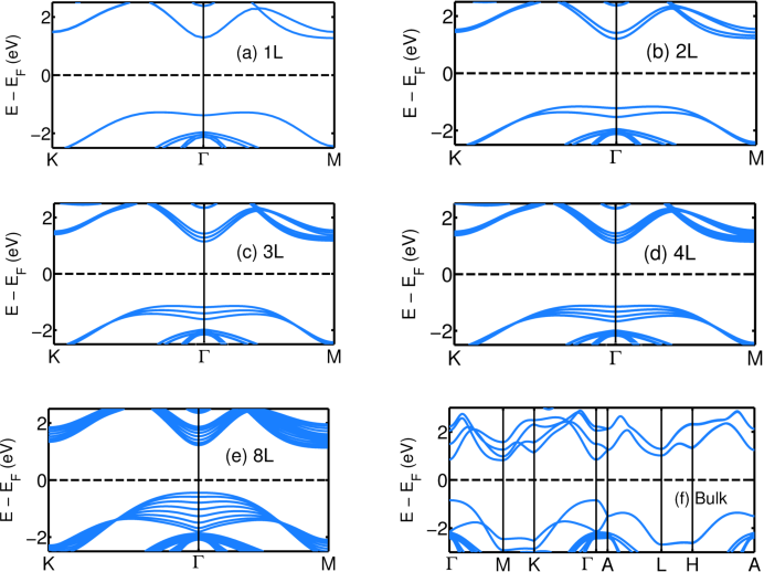
In this study, the default stacking is the phase illustrated in Fig. 2a. The phase is isostructural to the AA’ stacking order in the 2H polytypes of the molybdenum and tungsten dichalcogenides.He et al. (2014) The bandgap of the one to four monolayer structures is indirect for GaS, GaSe, InS and InSe. Figure 3 illustrates the PBE band structure for one-layer (1L) through four-layers (4L), eight-layer (8L) and bulk GaS.
The PBE SOC band gaps and energy transitions for each of the III-VI materials and film thicknesses are are listed in Table 2. For GaS, the HSE SOC values are also listed. The effective masses extracted from the PBE SOC electronic bandstructure are listed in Table 3.
| Structure | Transition | GaS | GaSe | InS | InSe |
|---|---|---|---|---|---|
| 1L | Ev to | 2.563 (3.707) | 2.145 | 2.104 | 1.618 |
| Ev to | 2.769 (3.502) | 2.598 | 2.684 | 2.551 | |
| Ev to | 2.549 (3.422) | 2.283 | 2.520 | 2.246 | |
| 2L | Ev to | 2.369 (3.156) | 1.894 | 1.888 | 1.332 |
| Ev to | 2.606 (3.454) | 2.389 | 2.567 | 2.340 | |
| Ev to | 2.389 (3.406) | 2.065 | 2.353 | 2.025 | |
| 3L | Ev to | 2.288 (3.089) | 1.782 | 1.789 | 1.152 |
| Ev to | 2.543 (3.408) | 2.302 | 2.496 | 2.201 | |
| Ev to | 2.321 (3.352) | 1.967 | 2.273 | 1.867 | |
| 4L | Ev to | 2.228 (3.011) | 1.689 | 1.749 | 1.086 |
| Ev to | 2.496 (3.392) | 2.224 | 2.471 | 2.085 | |
| Ev to | 2.267 (3.321) | 1.879 | 2.242 | 1.785 | |
| Bulk | to | 1.691 (2.705) | 0.869 | 0.949 | 0.399 |
| to | 1.983 (2.582) | 1.435 | 1.734 | 1.584 | |
| to | 1.667 (2.391) | 0.964 | 1.400 | 1.120 |
| Structure | GaS | GaSe | InS | InSe | GaS | GaSe | InS | InSe |
|---|---|---|---|---|---|---|---|---|
| Hole Effective Mass (m0) | Electron Effective Mass (m0) | |||||||
| 1L | 0.409 | 0.544 | 0.602 | 0.912 | 0.067 (0.698) | 0.053 | 0.080 | 0.060 |
| 2L | 0.600 | 0.906 | 0.930 | 1.874 | 0.065 (0.699) | 0.051 | 0.075 | 0.055 |
| 3L | 0.746 | 1.439 | 1.329 | 6.260 | 0.064 (0.711) | 0.050 | 0.074 | 0.053 |
| 4L | 0.926 | 2.857 | 1.550 | 3.611 | 0.064 (0.716) | 0.049 | 0.073 | 0.055 |
The conduction bands of GaSe, InS, and InSe are at for all layer thicknesses, from monolayer to bulk. The conduction band of monolayer GaS is at M. This result is consistent with that of Zólyomi et al.Zolyomi et al. (2013). However, for all thicknesses greater than a monolayer, the conduction band of GaS is at . Results from the PBE functional give GaS conduction valley separations between M and that are on the order of at room temperature, and this leads to qualitatively incorrect results in the calculation of the electronic and thermoelectric parameters. For the three other III-VI compounds, the minimum PBE-SOC spacing between the conduction and M valleys is 138 meV in monolayer GaSe. For InS and InSe, the minimum conduction -M valley separations also occur for a monolayer, and they are 416 eV and 628 eV, respectively. For monolayer GaS, the HSE-SOC conduction M valley lies 80 meV below the K valley and 285 meV below the valley. At two to four layer thicknesses, the order is reversed, the conduction band edge is at , and the energy differences between the valleys increase. For the electronic and thermoelectric properties, only energies within a few of the band edges are important. Therefore, the density of modes of n-type GaS is calculated from the HSE-SOC bandstructure. For p-type GaS and all other materials, the densities of modes are calculated from the PBE-SOC bandstructure.
The orbital composition of the monolayer GaS conduction valley contains 63% Ga orbitals and 21% S orbitals. The orbital compositions of the other III-VI conduction valleys are similar. As the film thickness increases from a monolayer to a bilayer, the conduction valleys in each layer couple and split by 203 meV as shown in Fig. 3b. Thus, as the film thickness increases, the number of low-energy states near the conduction band-edge remains the same, or, saying it another way, the number of low-energy states per unit thickness decreases by a factor of two as the the number of layers increases from a monolayer to a bilayer. This affects the electronic and thermoelectric properties.
The Mexican hat feature of the valence band is present in all of the 1L - 4L GaX and InX structures, and it is most pronounced for the monolayer structure shown in Fig. 3a. For monolayer GaS, the highest valence band at is composed of 79% sulfur orbitals (). The lower 4 valence bands at are composed entirely of sulfur and orbitals (). When multiple layers are brought together, the valence band at strongly couples and splits with a splitting of 307 meV in the bilayer. For the 8-layer structure in Fig. 3e, the manifold of 8 bands touches the manifold of bands, and the bandstructure is bulklike with discrete momenta. In the bulk shown in Fig. 3f, the discrete energies become a continuous dispersion from to . At 8 layer thickness, the large splitting of the valence band removes the Mexican hat feature, and the valence band edge is parabolic as in the bulk. The nature and orbital composition of the bands of the 4 III-VI compounds are qualitatively the same.
| Material | (meV) | (nm-1) |
|---|---|---|
| (Theory/Stacking Order) | 1L, 2L, 3L, 4L | 1L, 2L, 3L, 4L |
| GaS | 111.2, 59.6, 43.8, 33.0 | 3.68, 2.73, 2.52, 2.32 |
| GaS (no-SOC) | 108.3, 60.9, 45.1, 34.1 | 3.16, 2.63, 2.32, 2.12 |
| GaS (HSE) | 97.9, 50.3, 40.9, 31.6 | 2.81, 2.39, 2.08, 1.75 |
| GaS (AA) | 111.2, 71.5, 57.1, 47.4 | 3.68, 2.93, 2.73, 2.49 |
| GaSe | 58.7, 29.3, 18.1, 10.3 | 2.64, 2.34, 1.66, 1.56 |
| GaSe () | 58.7, 41.2, 23.7 , 5.1 | 2.64, 1.76, 1.17 , 1.01 |
| InS | 100.6, 44.7, 25.8, 20.4 | 4.03, 3.07, 2.69, 2.39 |
| InSe | 34.9, 11.9, 5.1, 6.1 | 2.55, 1.73, 1.27, 1.36 |
| InSe (HSE) | 38.2, 15.2, 8.6, 9.2 | 2.72, 2.20, 1.97, 2.04 |
| Bi2Se3 | 314.7, 62.3, 12.4, 10.4 | 3.86, 1.23, 1.05, 0.88 |
| Bi2Se3 (no-SOC) | 350.5, 74.6, 22.8, 20.1 | 4.19, 1.47, 1.07, 1.02 |
In the few-layer structures, the Mexican hat feature of the valence band can be characterized by the height, , at and the radius of the band-edge ring, , as illustrated in Figure 2(b). The actual ring has a small anisotropy that has been previously characterized and discussed in detail Zolyomi et al. (2013, 2014); Cao et al. (2014). For all four III-VI compounds of monolayer and few-layer thicknesses, the valence band maxima (VBM) of the inverted Mexican hat lies along , and it is slightly higher in energy compared to the band extremum along . In monolayer GaS, the valence band maxima along is 4.7 meV above the band extremum along . In GaS, as the film thickness increases from one layer to four layers the energy difference between the two extrema decreases from 4.7 meV to 0.41 meV. The maximum energy difference of 6.6 meV between the band extrema of the Mexican hat occurs in a monolayer of InS. In all four III-VI compounds the energy difference between the band extrema is maximum for the monolayer structure and decreases below 0.5 meV in all of the materials for the four-layer structure. The tabulated values of in Table 4 give the distance from to the VBM in the direction. Results calculated from PBE and HSE functionals are given, and results with and without spin-orbit coupling are listed. The effects of AA’ versus AA stacking order of GaS and AA’ versus stacking order of GaSe Zhu et al. (2012); An et al. (2014) are also compared.
Table 4 shows that the valence band Mexican hat feature is robust. It is little affected by the choice of functional, the omission or inclusion of spin-orbit coupling, or the stacking order. A recent study of GaSe at the G0W0 level found that the Mexican hat feature is also robust against many-electron self-energy effects.Cao et al. (2014) For all materials, the values of and are largest for monolayers and decrease as the film thicknesses increase. This suggests that the height of the step function density of modes will also be maximum for the monolayer structures.
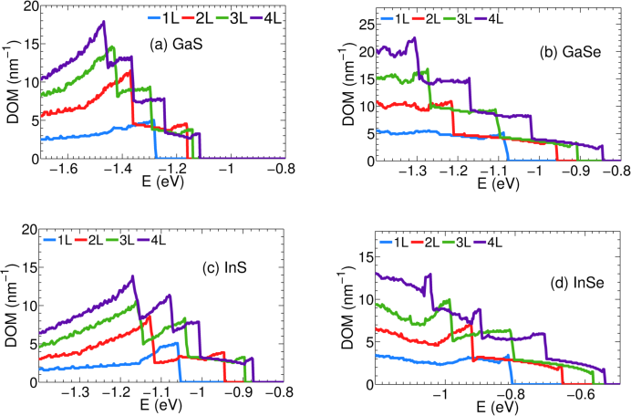
Figure 4 illustrates the valence band density of modes for 1L, 2L, 3L and 4L GaS, GaSe, InS and InSe. The valence band density of modes is a step function for the few-layer structures, and the height of the step function at the valence band edge is reasonably approximated by Eq. (15). The height of the numerically calculated density of modes step function for monolayer GaS, GaSe, InS and InSe is 4.8 nm-1, 5.2 nm-1, 5.1 nm-1 and 3.4 nm-1 respectively. Using the values for and Eq. (15) and accounting for spin degeneracy, the height of the step function for monolayer GaS, GaSe, InS and InSe is 4.1 nm-1, 3.4 nm-1, 5.1 nm-1 and 3.2 nm-1. The height of the numerically calculated density of modes in GaS decreases by when the film thickness increases from one to four monolayers, and the value of decreases by . The height of the step function using Eq. (15) and is either underestimated or equivalent to the numerical density of modes. For all four materials GaS, GaSe, InS and InSe, decreasing the film thickness increases and the height of the step-function of the band-edge density of modes. A larger band-edge density of modes gives a larger power factor and ZT compared to that of the bulk.
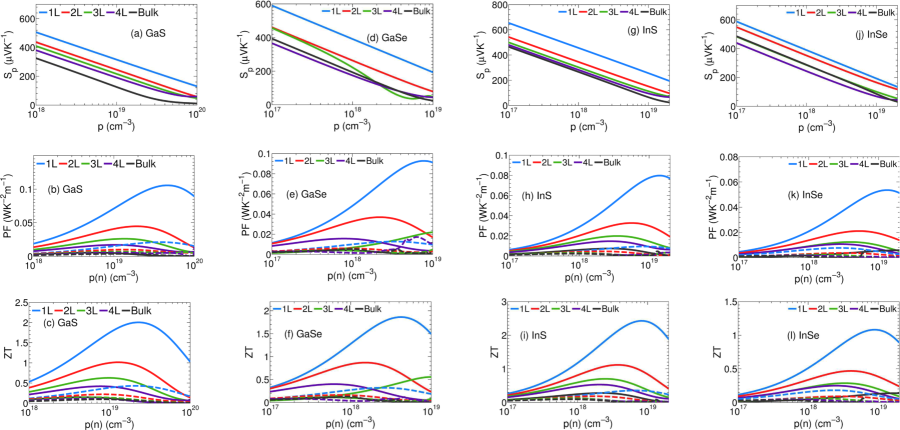
The p-type Seebeck coefficients, the p-type and n-type power factors, and the thermoelectric figures-of-merit (ZT) as functions of carrier concentration at room temperature for GaS, GaSe, InS and InSe are shown in Figure 5. The thermoelectric parameters at K of bulk and one to four monolayers of GaS, GaSe, InS and InSe are summarized in Tables 5 - 8. For each material the peak p-type ZT occurs at a monolayer thickness. The largest room temperature p-type ZT occurs in monolayer InS. At room temperature, the peak p-type (n-type) ZT values in 1L, 2L, 3L and 4L GaS occur when the Fermi level is 42 meV, 38 meV, 34 meV and 30 meV (22 meV, 17 meV, 11 meV, and 7 meV) above (below) the valence (conduction) band edge, and the Fermi level positions in GaSe, InS and InSe change in qualitatively the same way. The p-type hole concentrations of monolayer GaS, GaSe, InS and InSe at the peak ZT are enhanced by factors of 9.7, 10.8, 7.2 and 5.5 compared to those of their respective bulk structures. At the peak p-type room-temperature ZT, the Seebeck coefficients of monolayer GaS, GaSe, InS and InSe are enhanced by factors of 1.3, 1.4, 1.3, and 1.3, respectively, compared to their bulk values. However, the monolayer and bulk peak ZT values occur at carrier concentrations that differ by an order of magnitude. At a fixed carrier concentration, the monolayer Seebeck coefficients are approximately 3.1 times larger than the bulk Seebeck coefficients. The p-type power factor (PF) at the peak ZT for 1L GaS is enhanced by a factor of 17 compared to that of bulk GaS. The p-type ZT values of monolayer GaS, GaSe, InS and InSe are enhanced by factors of 14.3, 16.9, 8.7 and 7.7, respectively, compared to their bulk values. At the peak p-type ZT, the contribution of to is minimum for the bulk structure and maximum for the monolayer structure. The contributions of to in bulk and monolayer GaS are 5% and 24%, respectively. The increasing contribution of to with decreasing film thickness reduces the enhancement of ZT relative to that of the power factor.
| Thickness | p | ZTp | n | —S | ZTe | |||
|---|---|---|---|---|---|---|---|---|
| (1019cm-3) | () | ( | (1019 cm-3) | () | ( | |||
| 1L | 3.19 | 251.6 | 1.41 | 2.01 | 1.02 | 237.0 | .348 | .431 |
| 2L | 1.51 | 222.9 | .776 | 1.02 | .621 | 219.6 | .229 | .218 |
| 3L | 1.13 | 213.2 | .530 | .630 | .595 | 200.9 | .206 | .147 |
| 4L | .922 | 211.2 | .390 | .421 | .545 | 191.9 | .195 | .111 |
| Bulk | .330 | 187.6 | .149 | .140 | .374 | 210.8 | .116 | .095 |
The increases in the Seebeck coefficients, the charge densities, and the electrical conductivities with decreases in the film thicknesses follow the increases in the magnitudes of and as discussed at the end of Sec. II.2. For bulk p-type GaS, the values of () at peak ZT are 0.94 (1.85), and for monolayer GaS, they are 8.87 (23.4). They increase by factors of 9.4 (12.6) as the film thickness decreases from bulk to monolayer. In 4L GaS, the values of () are 2.45 (5.38), and they increase by factors of 3.6 (5.4) as the thickness is reduced from 4L to 1L. For all four of the III-VI compounds, the increases in are larger than the increases in as the film thicknesses decrease. As described in Sec. II.2, these increases are driven by the transformation of the dispersion from parabolic to Mexican hat with an increasing radius of the band edge -space ring as the thickness is reduced from bulk to monolayer.
| Thickness | p | ZTp | n | —S | ZTe | |||
|---|---|---|---|---|---|---|---|---|
| (1018cm-3) | () | ( | (1018 cm-3) | () | ( | |||
| 1L | 5.81 | 256.1 | 1.28 | 1.86 | 2.71 | 202.9 | .310 | .321 |
| 2L | 2.70 | 225.3 | .711 | .870 | 1.20 | 201.4 | .152 | .162 |
| 3L | 2.09 | 221.2 | .450 | .561 | .79 | 194.0 | .103 | .110 |
| 4L | 1.49 | 210.2 | .352 | .391 | .69 | 186.4 | .085 | .082 |
| Bulk | .541 | 180.9 | .121 | .112 | .29 | 127.9 | .033 | .132 |
While the focus of the paper is on the effect of the Mexican hat dispersion that forms in the valence band of these materials, the n-type thermoelectric figure of merit also increases as the film thickness is reduced to a few layers, and it is also maximum at monolayer thickness. The room temperature, monolayer, n-type thermoelectric figures of merit of GaS, GaSe, InS and InSe are enhanced by factors of 4.5, 2.4, 3.8 and 5.3, respectively, compared to the those of the respective bulk structures. The largest n-type ZT occurs in monolayer GaS. In a GaS monolayer, the 3-fold degenerate M valleys form the conduction band edge. This large valley degeneracy gives GaS the largest n-type ZT among the 4 III-VI compounds. As the GaS film thickness increases from a monolayer to a bilayer, the conduction band edge moves to the non-degenerate valley so that the number of low-energy states near the conduction band edge decreases. With an added third and fourth layer, the M valleys move higher, and the valley continues to split so that the number of low-energy conduction states does not increase with film thickness. Thus, for a Fermi energy fixed slightly below the band edge, the electron density and the conductivity decrease as the number of layers increase as shown in Tables 5 - 8. As a result, the maximum n-type ZT for each material occurs at a single monolayer and decreases with each additional layer.
| Thickness | p | ZTp | n | —S | ZTe | |||
|---|---|---|---|---|---|---|---|---|
| (1018cm-3) | () | ( | (1018 cm-3) | () | ( | |||
| 1L | 9.30 | 244.2 | 1.26 | 2.43 | 3.75 | 210.8 | .210 | .350 |
| 2L | 4.20 | 228.7 | .610 | 1.12 | 1.63 | 200.0 | .113 | .181 |
| 3L | 2.32 | 229.5 | .361 | .701 | 1.25 | 196.9 | .078 | .120 |
| 4L | 1.91 | 222.0 | .292 | .532 | 1.02 | 198.1 | .059 | .094 |
| Bulk | 1.30 | 195.1 | .180 | .280 | 1.21 | 179.8 | .070 | .092 |
| Thickness | p | ZTp | n | —S | ZTe | |||
|---|---|---|---|---|---|---|---|---|
| (1018cm-3) | () | ( | (1018 cm-3) | () | ( | |||
| 1L | 9.71 | 229.8 | .981 | 1.08 | 2.34 | 200.5 | .192 | .180 |
| 2L | 4.04 | 219.8 | .430 | .471 | 1.22 | 194.7 | .111 | .090 |
| 3L | 4.18 | 204.2 | .471 | .292 | .781 | 189.1 | .067 | .059 |
| 4L | 2.45 | 201.0 | .261 | .252 | .610 | 186.8 | .053 | .045 |
| Bulk | 1.75 | 179.1 | .181 | .142 | .652 | 160.9 | .054 | .034 |
IV.2 Bi2Se3
Bi2Se3 is an iso-structural compound of the well known thermoelectric, Bi2Te3. Both materials have been intensely studied recently because they are also topological insulators.Chen et al. (2009); Yin et al. (2013b); Hseih et al. (2008) Bulk Bi2Se3 has been studied less for its thermoelectric properties due to its slightly higher thermal conductivity compared to Bi2Te3. The bulk thermal conductivity of Bi2Se3 is 2 W-(mK)-1 compared to a bulk thermal conductivity of 1.5 W-(mK)-1 reported for Bi2Te3. Goldsmid (2009); Goyal et al. (2010) However, the thermoelectric performance of bulk Bi2Te3 is limited to a narrow temperature window around room temperature because of its small bulk band gap of approximately 160 meV.Chen et al. (2009) The band gap of single quintuple layer (QL) Bi2Te3 was previously calculated to be 190 meV.Zahid and Lake (2010) In contrast, the bulk bandgap of Bi2Se3 is 300 meV Checkelsky et al. (2011) which allows it to be utilized at higher temperatures.
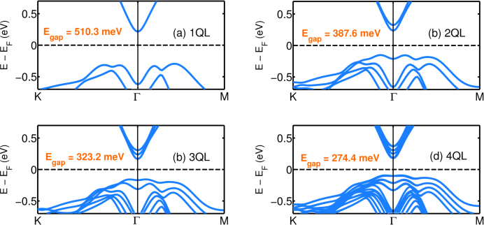
The optimized lattice parameters for bulk Bi2Se3 are listed in Table 1. The optimized bulk crystal structure and bulk band gap is consistent with prior experimental and theoretical studies of bulk Bi2Se3. Nakajima (1963); Saeed et al. (2014) Using the optimized lattice parameters of the bulk structure, the electronic structures of one to four quintuple layers of Bi2Se3 are calculated with the inclusion of spin-orbit coupling. The electronic structures of 1 to 4 QLs of Bi2Se3 are shown in Figure 6. The band gaps for one to four quintuple layers of Bi2Se3 are 510 meV, 388 meV, 323 meV and 274 meV for the 1QL, 2QL, 3QL and 4QL films, respectively. The effective masses of the conduction and valence band at for 1QL to 4QL of Bi2Se3 are listed in Table 9.
For each of the thin film structures, the conduction bands are parabolic and located at . The conduction band at of the 1QL structure is composed of 13 Se , 24 Se , 16 Bi , and 39 Bi . The orbital composition of the valley remains qualitatively the same as the film thickness increases to 4QL. The orbital composition of the bulk conduction band is 79 Se and 16 Bi . As the film thickness increases above 1QL, the conduction band at splits, as illustrated in Figs. 6(b)-(d). In the 2QL, 3QL and 4QL structures the conduction band splitting varies between 53.9 meV and 88.2 meV. As with the III-VIs, the number of low-energy conduction band states per unit thickness decreases with increasing thickness.
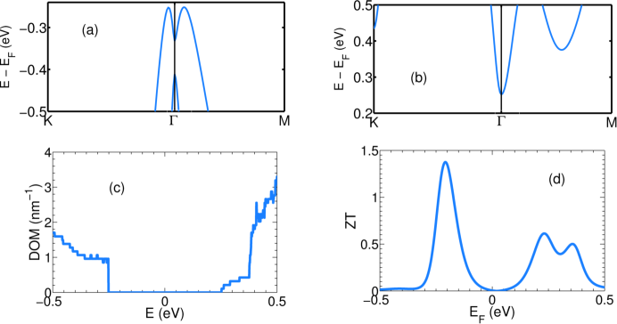
The valence bands have slightly anistropic Mexican hat dispersions. The values of and used to characterize the Mexican hat for the 1QL to 4QL structures of Bi2Se3 are listed in Table 4. The radius k0 is the distance from to the band extremum along , which is the valence band maxima for the 1QL to 4QL structures. The energy difference between the valence band maxima and the band extremum along decreases from 19.2 meV to 0.56 meV as the film thickness increases from 1QL to 4QL. The Mexican hat dispersion in 1QL of Bi2Se3 is better described as a double brimmed hat consisting of two concentric rings in -space characterized by four points of extrema that are nearly degenerate. The band extremum along adjacent to the valence band maxima, is 36 meV below the valence band maxima. Along the energy difference between the two band extrema is 4.2 meV. At , the orbital composition of the valence band for 1QL of Bi2Se3 is 63 pz orbitals of Se, 11 pxy orbitals of Se and 18 s orbitals of Bi, and the orbital composition remains qualitatively the same as the film thickness increases to 4QL. As the thickness increases above a monolayer, the energy splitting of the valence bands from each layer is large with respect to room temperature and more complex than the splitting seen in the III-VIs. At a bilayer, the highest valence band loses most of the outer -space ring, the radius decreases by a factor 3.1 and the height () of the hat decreases by a factor of 5.1. This decrease translates into a decrease in the initial step height of the density of modes shown in Figure 7(a). The second highest valence band retains most of the shape of the original monolayer valence band, but it is now too far from the valence band edge to contribute to the low-energy electronic or thermoelectric properties. Thus, Bi2Se3 follows the same trends as seen in Bi2Te3; the large enhancement in the thermoelectric properties resulting from bandstructure are only significant for a monolayer Maassen and Lundstrom (2013).
| Structure | (m0) | (m0) |
|---|---|---|
| 1L | 0.128 | 0.132 |
| 2L | 0.436 | 0.115 |
| 3L | 1.435 | 0.176 |
| 4L | 1.853 | 0.126 |
| Thickness | p | ZTp | n | —S | ZTe | |||
|---|---|---|---|---|---|---|---|---|
| (1018cm-3) | () | ( | (1018 cm-3) | () | ( | |||
| 1L | 7.66 | 279.3 | .371 | 2.86 | 4.63 | 210.1 | .067 | .411 |
| 2L | 4.65 | 251.3 | .282 | 1.17 | 3.38 | 208.2 | .049 | .271 |
| 3L | 2.77 | 259.4 | .172 | 1.12 | 2.96 | 198.3 | .043 | .232 |
| 4L | 2.58 | 237.8 | .161 | .942 | 2.56 | 185.8 | .037 | .190 |
| Bulk | 1.95 | 210.7 | .095 | .521 | 1.23 | 191.9 | .020 | .123 |
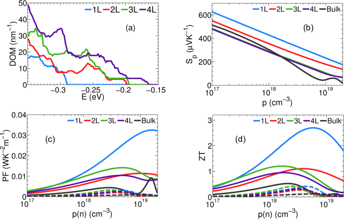
The p-type and n-type Seebeck coefficient, electrical conductivity, power factor and the thermoelectric figure-of-merit (ZT) as a function of carrier concentration at room temperature for Bi2Se3 are illustrated in Figure 7. The thermoelectric parameters at K of bulk and one to four quintuple layers for Bi2Se3 are summarized in Table 10.
The p-type ZT for the single quintuple layer is enhanced by a factor of 5.5 compared to that of the bulk film. At the peak ZT, the hole concentration is 4 times larger than that of the bulk, and the position of the Fermi energy with respect to the valence band edge () is 45 meV higher than that of the bulk. The bulk and monolayer magnitudes of () are 0.88 (2.14) and 3.45 (11.2), respectively, giving increases of 3.9 (5.2) as the thickness is reduced from bulk to monolayer. As the film thickness is reduced from 4 QL to 1 QL, the magnitudes of and at the peak ZT increase by factors of 2.4 and 2.8, respectively.
The peak room temperature n-type ZT also occurs for 1QL of Bi2Se3. In one to four quintuple layers of Bi2Se3, two degenerate bands at contribute to the conduction band density of modes. The higher valleys contribute little to the conductivity as the film thickness increases. The Fermi levels at the peak n-type, room-temperature ZT rise from 34 meV to 12 meV below the conduction band edge as the film thickness increases from 1 QL to 4 QL while the electron density decreases by a factor of 1.8. This results in a maximum n-type ZT for the 1QL structure.
A recent study on the thickness dependence of the thermoelectric properties of ultra-thin Bi2Se3 obtained a p-type ZT value of 0.27 and a p-type peak power factor of 0.432 mWm-1K-2 for the 1QL film. Saeed et al. (2014) The differences in the power factor and the ZT are due to the different approximations made in the relaxation time (2.7 fs) and lattice thermal conductivity (0.49 W/mK) used in this study. Using the parameters of Ref.[Saeed et al., 2014] in our density of modes calculation of 1QL of Bi2Se3 gives a peak p-type ZT of 0.58 and peak p-type power factor of 0.302 mWm-1K-2. We also compare the thermoelectric properties of single quintuple layer Bi2Se3 and Bi2Te3. In both materials, the valence band of the single quintuple film is strongly deformed into a Mexican hat. The radius for 1QL of Bi2Se3 is a factor of 2 higher than for 1QL Bi2Te3. The peak p-type ZT of 7.15 calculated for Bi2Te3 Zahid and Lake (2010) is a factor of 2.5 higher than the peak p-type ZT of 2.86 obtained for a single quintuple layer of Bi2Se3. This difference in the thermoelectric figure of merit can be attributed to the different approximations in the hole mean free path chosen for Bi2Se3 (=2.4 nm) and Bi2Te3 (=8 nm) Zahid and Lake (2010) and the higher lattice thermal conductivity of Bi2Se3 (=2 W/mK) compared to Bi2Te3 (=1.5 W/mK).
IV.3 Bilayer Graphene
AB stacked bilayer graphene (BLG) is a gapless semiconductor with parabolic conduction and valence bands that are located at the () symmetry points. Prior experimental Zhang et al. (2009); Varlet et al. (2014) and theoretical Min et al. (2007) studies demonstrated the formation of a bandgap in BLG with the application of a vertical electric field. The vertical electric field also deforms the conduction and valence band edges at into a Mexican-hat dispersion Stauber et al. (2007); Varlet et al. (2014). Using ab-initio calculations we compute the band structure of bilayer graphene subject to vertical electric fields ranging from 0.05 V/Å to 0.5 V/Å. The lattice parameters for the bilayer graphene structure used in our simulation are given in Table 1. The ab-initio calculated band gaps are in good agreement with prior calculations. Min et al. (2007); McCann (2006) The bandgap increases from 144.4 meV to 277.3 meV as the applied field increases from 0.05 V/Å to 0.5 V/Å.
For each applied field ranging from from 0.05 V/Å to 0.5 V/Å both the valence band and the conduction band edges lie along the path , and the radius is the distance from to the band edge along . The magnitude of increases linearly with the electric field as shown in Figure 8(a). The dispersions of the valence band and the conduction band quantitatively differ, and of the valence band is up to 20 higher than of the conduction band. The anisotropy of the conduction and valence Mexican hat dispersions increase with increasing vertical field. The extremum point along of the valence (conduction) band Mexican hat dispersion is lower (higher) in energy compared to the band extremum along . As the field increases from 0.05 V/Å to 0.5 V/Å the energy difference between the two extrema points increases from 5.2 meV to 69.4 meV in the valence band and 7.7 meV to 112.3 meV in the conduction band. This anisotropy in the Mexican hat of the valence and conduction band leads to a finite slope in the density of modes illustrated in Figure 8(b).
As the applied field is increased from 0.05 V/Å to 0.5 V/Å the height of the density of modes step function in the valence and conduction band increases by a factor of 5.7. Figure 8(b) illustrates the density of modes distribution for the conduction and valence band states for the lowest field applied (0.05 V/Å) and the highest field applied (0.5 V/Å). The p-type thermoelectric parameters of bilayer graphene subject to vertical electric fields ranging from 0.05 V/Å to 0.5 V/Å are summarized in Table 11. The p-type and n-type thermoelectric parameters are similar. Figure 8(d) compares the calculated ZT versus Fermi level for bilayer graphene at applied electric fields of 0.05 V/Å to 0.5 V/Å. For an applied electric field of 0.5 V/Å the p-type and n-type ZT is enhanced by a factor of 6 and 4 in bilayer graphene compared to the ZT of bilayer graphene with no applied electric field.
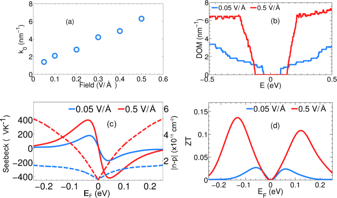
| Field | p | ZTp | ||
|---|---|---|---|---|
| (V/Å) | ( cm-2) | () | ||
| 0.0 | .12 | 138.4 | .83 | .0230 |
| 0.05 | .11 | 154.9 | .77 | .0270 |
| 0.1 | .16 | 192.1 | 1.1 | .0281 |
| 0.2 | .19 | 190.7 | 1.3 | .0693 |
| 0.3 | .21 | 179.8 | 1.4 | .0651 |
| 0.4 | .27 | 196.4 | 1.8 | .1001 |
| 0.5 | .31 | 188.0 | 2.1 | .1401 |
IV.4 Bi Monolayer
The large spin-orbit interaction in bismuth leads to a Rasha-split dispersion of the valence band in a single monolayer of bismuth. The lattice parameters for the Bi(111) monolayer used for the SOC ab-initio calculations are summarized in Table 1. The bandgap of the bismuth monolayer is 503 meV with the conduction band at . The inclusion of spin-orbit interaction splits the two degenerate bands at by 79 meV and deforms the valence band maxima into a Rashba split band. The calculated band structure of the Bi(111) monolayer is shown in Figure 9(a,b).
The Rashba parameter for the bismuth monolayer is extracted from the ab-initio calculated band structure. The curvature of the valence band maxima of the Rashba band gives an effective mass of . The vertical splitting of the bands at small gives an eVÅ. Prior experimental and theoretical studies on the strength of the Rashba interaction in Bi(111) surfaces demonstrate values ranging from 0.55 eVÅ-1 to 3.05 eVÅ-1 . Ishizaka et al. (2011) A slight asymmetry in the Rashba-split dispersion leads to the valence band maxima lying along . The band extremum along is 0.5 meV below the valence band maxima. The radius of the valence band-edge , which is the distance from to the band extremum along is 1.40 nm-1 similar to 4L InSe. The valence band-edge density of modes shown in Fig. 9(c) is a step function with a peak height of 0.96 nm-1. Figure 9(d) shows the resulting thermoelectric figure of merit ZT as a function of Fermi level position at room temperature. The thermoelectric parameters at K are summarized in Table 12.
| p | ZTp | n | —S | ZTe | |||
| (1019cm-3) | () | ( | (1019 cm-3) | () | ( | ||
| .61 | 239.7 | .39 | 1.38 | .35 | 234.1 | .19 | .61 |
Using mean free paths of =50nm for electrons and =20nm for holes, our peak ZT values are consistent with a prior report on the thermoelectric properties of monolayer Bi.Cheng et al. (2013). The peak p-type (n-type) ZT and Seebeck values of 2.3 (1.9) and 786 V/K (-710 V/K) are consistent with reported values of 2.4 (2.1) and 800 V/K (-780 V/K) in Ref.[Cheng et al., 2013].
V Summary and Conclusions
Monolayer and few-layer structures of III-VI materials (GaS, GaSe, InS, InSe), Bi2Se3, monolayer Bi, and biased bilayer graphene all have a valence band that forms a ring in -space. For monolayer Bi, the ring results from Rashba splitting of the spins. All of the other few-layer materials have valence bands in the shape of a ‘Mexican hat.’ For both cases, a band-edge that forms a ring in -space is highly degenerate. It coincides with a singularity in the density of states and a near step-function turn-on of the density of modes at the band edge. The height of the step function is approximately proportional to the radius of the -space ring.
The Mexican hat dispersion in the valence band of the III-VI materials exists for few-layer geometries, and it is most prominent for monolayers, which have the largest radius and the largest height . The existence of the Mexican hat dispersions and their qualitative features do not depend on the choice of functional, stacking, or the inclusion or omission of spin-orbit coupling, and recent calculations by others show that they are also unaffected by many-electron self-energy effects.Cao et al. (2014) At a thickness of 8 layers, all of the III-VI valence band dispersions are parabolic.
The Mexican hat dispersion in the valence band of monolayer Bi2Se3 is qualitatively different from those in the monolayer III-VIs. It can be better described as a double-brimmed hat characterized by 4 points of extrema that lie within of each other at room temperature. Futhermore, when two layers are brought together to form a bilayer, the energy splitting of the two valence bands in each layer causes the highest band to lose most of its outer ring causing a large decrease in the density of modes and reduction in the thermoelectric properties. These trends also apply to Bi2Te3. Maassen and Lundstrom (2013)
The valence band of monolayer Bi also forms a -space ring that results from Rashba splitting of the bands. The diameter of the ring is relatively small compared to those of monolayer Mexican hat dispersions. However, the ring is the most isotropic of all of the monolayer materials considered, and it gives a very sharp step function to the valence band density of modes.
As the radius of the -space ring increases, the Fermi level at the maximum power factor or ZT moves higher into the bandgap away from the valence band edge. Nevertheless, the hole concentration increases. The average energy carried by a hole with respect to the Fermi energy increases. As a result, the Seebeck coefficient increases. The dispersion with the largest radius coincides with the maximum power factor provided that the mean free paths are not too different. For the materials and parameters considered here, the dispersion with the largest radius also results in the largest ZT at room temperature. Bilayer graphene may serve as a test-bed to measure these effects, since a cross-plane electric field linearly increases the diameter of the Mexican hat ring, and the features of the Mexican hat in bilayer graphene have recently been experimentally observed.Varlet et al. (2014)
With the exception of monolayer GaS, the conduction bands of few-layer n-type III-VI and Bi2Se3 compounds are at with a significant orbital component. In bilayers and multilayers, these bands couple and split pushing the added bands to higher energy above the thermal transport window. Thus, the number of low-energy states per layer is maximum for a monolayer. In monolayer GaS, the conduction band is at M with 3-fold valley degeneracy. At thicknesses greater than a monolayer, the GaS conduction band is at , the valley degeneracy is one, and the same splitting of the bands occurs as described above. Thus, the number of low-energy states per layer is also maximum for a monolayer GaS. This results in maximum values for the n-type Seebeck coefficients, power factors, and ZTs at monolayer thicknesses for all of these materials.
Acknowledgements.
This work is supported in part by the National Science Foundation (NSF) Grant Nos. 1124733 and the Semiconductor Research Corporation (SRC) Nanoelectronic Research Initiative as a part of the Nanoelectronics for 2020 and Beyond (NEB-2020) program, FAME, one of six centers of STARnet, a Semiconductor Research Corporation program sponsored by MARCO and DARPA. This work used the Extreme Science and Engineering Discovery Environment (XSEDE), which is supported by National Science Foundation grant number OCI-1053575.References
- Mak et al. (2010) K. F. Mak, C. Lee, J. Hone, J. Shan, and T. F. Heinz, Phys. Rev. Lett. 105, 136805 (2010), URL http://link.aps.org/doi/10.1103/PhysRevLett.105.136805.
- Stauber et al. (2007) T.Stauber, N.M.R.Peres, F.Guinea, and A. H. CastroNeto, Physical Review B 75, 115425 (2007).
- Zolyomi et al. (2013) V. Zolyomi, N.D. Drummond, and V.I. Fal’ko, Physical Review B 87, 195403 (2013).
- Zolyomi et al. (2014) V. Zolyomi, N. D. Drummond, and V. I. Fal’ko, Phys. Rev. B 89, 205416 (2014), URL http://link.aps.org/doi/10.1103/PhysRevB.89.205416.
- Zhang et al. (2010) F. Zhang, B. Sahu, H. Min, and A. H. MacDonald, Physical Review B 82, 035409 (2010).
- Varlet et al. (2014) A. Varlet, D. Bischoff, P. Simonet, K. Watanabe, T. Taniguchi, T. Ihn, K. Ensslin, M. Mucha-Kruczyński, and V. I. Fal’ko, Phys. Rev. Lett. 113, 116602 (2014), URL http://link.aps.org/doi/10.1103/PhysRevLett.113.116602.
- Blanter et al. (1994) Y. M. Blanter, M. Kaganov, A. Pantsulaya, and A. Varlamov, Physics Reports 245, 159 (1994).
- Wang et al. (2014) X. Wang, L. Wang, J. Liu, and L. Peng, Applied Physics Letters 104, 132106 (2014).
- Peng et al. (2014) H. Peng, N. Kioussis, and G. J. Snyder, Physical Review B 89, 195206 (2014).
- Hu et al. (2013) P. Hu, L. Wang, M. Yoon, J. Zhang, W. Feng, X. Wang, Z. Wen, J. C. Idrobo, Y. Miyamoto, D. B. Geohegan, et al., Nano Letters 13, 1649 (2013).
- Zhuang and Hennig (2013) H. L. Zhuang and R. G. Hennig, Chemistry of Materials 25, 3232 (2013).
- Cao et al. (2014) T. Cao, Z. Li, and S. G. Louie, arXiv preprint arXiv:1409.4112 (2014).
- Wu et al. (2014) S. Wu, X. Dai, H. Yu, H. Fan, J. Hu, and W. Yao, arXiv preprint arXiv:1409.4733 (2014).
- Lei et al. (2013) S. Lei, L. Ge, Z. Liu, S. Najmaei, G. Shi, G. You, J. Lou, R. Vajtai, and P. M. Ajayan, Nano Letters 13, 2777 (2013).
- Lei et al. (2014) S. Lei, L. Ge, S. Najmaei, A. George, R. Kappera, J. Lou, M. Chhowalla, H. Yamaguchi, G. Gupta, R. Vajtai, et al., ACS Nano (2014).
- Hu et al. (2012) P. Hu, Z. Wen, L. Wang, P. Tan, and K. Xiao, ACS Nano 6, 5988 (2012).
- Late et al. (2012) D. J. Late, B. Liu, J. Luo, A. Yan, H. Matte, M. Grayson, C. Rao, and V. P. Dravid, Advanced Materials 24, 3549 (2012).
- Li et al. (2014) X. Li, M.-W. Lin, A. A. Puretzky, J. C. Idrobo, C. Ma, M. Chi, M. Yoon, C. M. Rouleau, I. I. Kravchenko, D. B. Geohegan, et al., Scientific reports 4 (2014).
- Mahjouri-Samani et al. (2014) M. Mahjouri-Samani, M. Tian, K. Wang, A. Boulesbaa, C. M. Rouleau, A. A. Puretzky, M. A. McGuire, B. R. Srijanto, K. Xiao, G. Eres, et al., ACS Nano (2014).
- Shen et al. (2009) G. Shen, D. Chen, P.-C. Chen, and C. Zhou, ACS Nano 3, 1115 (2009).
- Zahid and Lake (2010) F. Zahid and R. Lake, Applied Physics Letters 97, 212102 (pages 3) (2010), URL http://link.aip.org/link/?APL/97/212102/1.
- Saeed et al. (2014) Y. Saeed, N. Singh, and U. Schwingenschlögl, Applied Physics Letters 104, 033105 (2014).
- Min et al. (2007) H. Min, B. Sahu, S. K. Banerjee, and A. H. MacDonald, Phys. Rev. B 75, 155115 (2007).
- Takayama et al. (2011) A. Takayama, T. Sato, S. Souma, and T. Takahashi, Physical Review Letters 106, 166401 (2011).
- Mahan and Sofo (1996) G. D. Mahan and J. O. Sofo, The Best Thermoelectric (National Academy of Sciences, Washington, DC, 1996), vol. 93, pp. 7436 – 7439.
- Heremans et al. (2008) J. P. Heremans, V. Jovovic, E. S. Toberer, A. Saramat, K. Kurosaki, A. Charoenphakdee, S. Yamanaka, and G. J. Snyder, Science 321, 554 (2008).
- Heremans et al. (2012) J. P. Heremans, B. Wiendlocha, and A. M. Chamoire, Energy & Environmental Science 5, 5510 (2012).
- Hicks and Dresselhaus (1993) L. D. Hicks and M. S. Dresselhaus, Phys. Rev. B 47, 16631 (1993), URL http://link.aps.org/doi/10.1103/PhysRevB.47.16631.
- Dresselhaus et al. (2007) M. S. Dresselhaus, G. Chen, M. Y. Tang, R. G. Yang, H. Lee, D. Z. Wang, Z. F. Ren, J.-P. Fleurial, and P. Gogna, Advanced Materials 19, 1043 (2007), ISSN 1521-4095, URL http://dx.doi.org/10.1002/adma.200600527.
- Pei et al. (2011) Y. Pei, X. Shi, A. LaLonde, H. Wang, L. Chen, and G. J. Snyder, Nature 473, 66 (2011).
- Sootsman et al. (2009) J. R. Sootsman, D. Y. Chung, and M. G. Kanatzidis, Angewandte Chemie 48, 8616 (2009).
- Fuccillo et al. (2013) M. K. Fuccillo, Q. D. Gibson, M. N. Ali, L. M. Schoop, and R. J. Cava, APL Materials 1, 062102 (2013), URL http://scitation.aip.org/content/aip/journal/aplmater/1/6/10.1063/1.4833055.
- Sun et al. (2009) P. Sun, N. Oeschler, S. Johnsen, B. B. Iversen, and F. Steglich, Applied Physics Express 2, 091102 (2009), URL http://stacks.iop.org/1882-0786/2/i=9/a=091102.
- Zhang et al. (2011) Y. Zhang, M. S. Dresselhaus, Y. Shi, Z. Ren, and G. Chen, Nano Letters 11, 1166 (2011).
- Maassen and Lundstrom (2013) J. Maassen and M. Lundstrom, Applied Physics Letters 102, 093103 (pages 4) (2013), URL http://link.aip.org/link/?APL/102/093103/1.
- Paul et al. (2012) A. Paul, S. Salamat, C. Jeong, G. Klimeck, and M. Lundstrom, Journal of Computational Electronics 11, 56 (2012), ISSN 1569-8025, URL http://dx.doi.org/10.1007/s10825-011-0379-2.
- Wickramaratne et al. (2014) D. Wickramaratne, F. Zahid, and R. K. Lake, The Journal of Chemical Physics 140, 124710 (2014).
- Datta (2005) S. Datta, Quantum Transport Atom to Transistor (Cambridge University Press, Cambridge, 2005).
- Jeong et al. (2010) C. Jeong, R. Kim, M. Luisier, S. Datta, and M. Lundstrom, Journal of Applied Physics 107, 023707 (pages 7) (2010), URL http://link.aip.org/link/?JAP/107/023707/1.
- Kim et al. (2009) R. Kim, S. Datta, and M. S. Lundstrom, Journal of Applied Physics 105, 034506 (pages 6) (2009), URL http://link.aip.org/link/?JAP/105/034506/1.
- Bychkov and Rashba (1984) Y. A. Bychkov and E. I. Rashba, Journal of physics C: Solid state physics 17, 6039 (1984).
- Ishizaka et al. (2011) K. Ishizaka, M. Bahramy, H. Murakawa, M. Sakano, T. Shimojima, T. Sonobe, K. Koizumi, S. Shin, H. Miyahara, A. Kimura, et al., Nature Materials 10, 521 (2011).
- Blöchl (1994) P. E. Blöchl, Phys. Rev. B 50, 17953 (1994).
- Perdew et al. (1996) J. P. Perdew, K. Burke, and M. Ernzerhof, Phys. Rev. Lett. 77, 3865 (1996).
- Ernzerhof and Scuseria (1999) M. Ernzerhof and G. E. Scuseria, J. Chem. Phys. 110, 5029 (1999).
- Kresse and Hafner (1993) G. Kresse and J. Hafner, Phys. Rev. B 48, 13115 (1993).
- Kresse and Furthmuller (1996) G. Kresse and J. Furthmuller, Comput. Mater. Sci. 6, 15 (1996).
- Grimme (2006) S. Grimme, Journal of Computational Chemistry 27, 1787 (2006), ISSN 1096-987X, URL http://dx.doi.org/10.1002/jcc.20495.
- Heyd et al. (2003) J. Heyd, G. E. Scuseria, and M. Ernzerhof, The Journal of Chemical Physics 118, 8207 (2003), URL http://scitation.aip.org/content/aip/journal/jcp/118/18/10.1063/1.1564060.
- Ismailov et al. (1966) F. I. Ismailov, G. A. Akhundov, and O. R. Vernich, Physica Status Solidi (b) 17, K237 (1966), ISSN 1521-3951, URL http://dx.doi.org/10.1002/pssb.19660170269.
- Micocci et al. (1990) G. Micocci, R. Rella, P. Siciliano, and A. Tepore, Journal of Applied Physics 68, 138 (1990).
- Krishna and Reddy (1983) D. Krishna and P. Reddy, Thin Solid Films 105, 139 (1983), ISSN 0040-6090, URL http://www.sciencedirect.com/science/article/pii/004060908390202X.
- Mane and Lokhande (2003) R. Mane and C. Lokhande, Materials Chemistry and Physics 78, 15 (2003).
- Cheng et al. (2013) L. Cheng, H. Liu, X. Tan, J. Zhang, J. Wei, H. Lv, J. Shi, and X. Tang, The Journal of Physical Chemistry C (2013).
- Yin et al. (2013a) G. Yin, D. Wickramaratne, and R. K. Lake, in Device Research Conference (DRC), 2013 71st Annual (IEEE, 2013a), pp. 69–70.
- Yin et al. (2014) G. Yin, D. Wickramaratne, Y. Zhao, and R. K. Lake, Applied Physics Letters 105, 033118 (2014), URL http://scitation.aip.org/content/aip/journal/apl/105/3/10.1063/1.4891574.
- Wang et al. (2011) C.-R. Wang, W.-S. Lu, L. Hao, W.-L. Lee, T.-K. Lee, F. Lin, I. ChunCheng, and J.-Z. Chen, Physical Review Letters 107, 186602 (2011).
- Jeong et al. (2012) C. Jeong, S. Datta, and M. Lundstrom, Journal of Applied Physics 111, 093708 (2012).
- Alzhdanov et al. (1999) M. Alzhdanov, M. Nadzhafzade, and Z. Y. Seidov, Physics of the Solid State 41, 20 (1999).
- Spitzer (1970) D. Spitzer, Journal of Physics and Chemistry of Solids 31, 19 (1970).
- Goldsmid (2009) H. J. Goldsmid, Introduction to Thermoelectricity, vol. 121 (Springer, 2009).
- Hor et al. (2009) Y. S. Hor, A. Richardella, P. Roushan, Y. Xia, J. G. Checkelsky, A. Yazdani, M. Z. Hasan, N. P. Ong, and R. J. Cava, Phys. Rev. B 79, 195208 (2009), URL http://link.aps.org/doi/10.1103/PhysRevB.79.195208.
- Balandin (2011) A. A. Balandin, Nature Materials 10, 569 (2011).
- Kong et al. (2009) B.D. Kong, S. Paul, M. B. Nardelli, and K. W. Kim, Physical Review B 80, 033406 (2009).
- Kuhn et al. (1976) A. Kuhn, A. Chevy, and R. Chevalier, Acta Crystallographica Section B: Structural Crystallography and Crystal Chemistry 32, 983 (1976).
- Kuhn et al. (1975) A. Kuhn, A. Chevy, and R. Chevalier, Physica Status Solidi (a) 31, 469 (1975).
- Ma et al. (2013) Y. Ma, Y. Dai, M. Guo, L. Yu, and B. Huang, Physical Chemistry Chemical Physics 15, 7098 (2013).
- De Blasi et al. (1982) C. De Blasi, G. Micocci, S. Mongelli, and A. Tepore, Journal of Crystal Growth 57, 482 (1982).
- Nakajima (1963) S. Nakajima, Journal of Physics and Chemistry of Solids 24, 479 (1963).
- Ohta et al. (2006) T. Ohta, A. Bostwick, T. Seyller, K. Horn, and E. Rotenberg, Science 313, 951 (2006).
- He et al. (2014) J. He, K. Hummer, and C. Franchini, Physical Review B 89, 075409 (2014).
- Zhu et al. (2012) Z. Zhu, Y. Cheng, and U. Schwingenschlögl, Physical Review Letters 108, 266805 (2012).
- An et al. (2014) W. An, F. Wu, H. Jiang, G.-S. Tian, and X.-Z. Li, The Journal of chemical physics 141, 084701 (2014).
- Chen et al. (2009) Y. L. Chen, J. G. Analytis, J.-H. Chu, Z. K. Liu, S.-K. Mo, X. L. Qi, H. J. Zhang, D. H. Lu, X. Dai, Z. Fang, et al., Science 325, 178 (2009), eprint http://www.sciencemag.org/content/325/5937/178.full.pdf, URL http://www.sciencemag.org/content/325/5937/178.abstract.
- Yin et al. (2013b) G. Yin, D. Wickramaratne, and R. K. Lake, Journal of Applied Physics 113, 063707 (2013b).
- Hseih et al. (2008) D. Hseih, D. Qian, L. Wray, Y. Xia, Y. S. Hor, R. J. Cava, and M. Z. Hasan, Nature 452, 970 (2008), URL http://www.nature.com/nature/journal/v452/n7190/suppinfo/nature06843_S1.html.
- Goyal et al. (2010) V. Goyal, D. Teweldebrhan, and A. A. Balandin, Applied Physics Letters 97, 133117 (pages 3) (2010), URL http://link.aip.org/link/?APL/97/133117/1.
- Checkelsky et al. (2011) J.G. Checkelsky, Y.S Hor, R.J. Cava, and N.P. Ong, Physical Review Letters 106, 196801 (2011).
- Zhang et al. (2009) Y. Zhang, T.-T. Tang, C. Girit, Z. Hao, M. C. Martin, A. Zettl, M. F. Crommie, Y. R. Shen, and F. Wang, Nature 459, 820 (2009).
- McCann (2006) E. McCann, Phys. Rev. B 74, 161403R (2006), URL dx.doi.org/10.1103/PhysRevB.74.161403.