Heat transfer coefficient saturation in superconducting Nb tunnel junctions contacted to a NbTiN circuit and an Au energy relaxation layer
Abstract
In this paper we present the experimental realization of a Nb tunnel junction connected to a high-gap superconducting NbTiN embedding circuit. We investigate relaxation of nonequilibrium quasiparticles in a small volume Au layer between the Nb tunnel junction and the NbTiN circuit. We find a saturation in the effective heat-transfer coefficient consistent with a simple theoretical model. This saturation is determined by the thickness of the Au layer. Our findings are important for the design of the ideal Au energy relaxation layer for practical SIS heterodyne mixers and we suggest two geometries, one, using a circular Au layer and, two, using a half-circular Au layer. Our work is concluded with an outlook of our future experiments.
Index Terms:
Heat transfer, Niobium SIS junctions, Nonequilibrium, SIS mixers, Superconductivity.I Introduction
In radio astronomy, heterodyne instruments are used to detect weak radiation from an astronomical source with a very high spectral resolution [1]. The central element of a heterodyne instrument is a mixer which has a strong nonlinear current-voltage (I-V) characteristic. In this article we will focus on superconductor-insulator-superconductor (SIS) tunnel junctions since they show a highly nonlinear I-V characteristic due to the singularity in the superconducting quasiparticle density-of-states and, therefore, perfectly fulfill the needs of a high-sensitivity astronomical heterodyne receiver. For a more complete review of other mixers, like the hot-electron bolometer mixer, we refer to [2].
The frequency mixing limit (i.e. the highest detectable frequency) in a SIS mixer is set by the superconducting pair-breaking energy . In this paper we focus on a symmetric SIS mixer which uses the same superconducting material for both junction electrodes. In such a device the frequency mixing limit is where is the Planck constant. Existing receivers almost enirely use Nb-Al-AlOx-Nb junctions, because they can be reliably fabricated with high quality, i.e. with very low subgap/leakage currents. Moreover, these devices already provide a reasonably high frequency mixing limit of theoretically 1.4 THz making them interesting for applications in radio-astronomy. In order to achieve the fundamental sensitivity limit of a SIS mixer [3], it is crucial that the tunnel junction is embedded in a high-Q tuning circuit that enables a near 100 % coupling to the sky signal. For this reason optimum embedding circuits are made of superconducting transmission lines. However, here lossless signal transport is provided only up to the superconducting pair-breaking frequency . Up to the pair-breaking frequency of niobium of approximately 700 GHz, the embedding circuit is made of the same material like the Nb junction electrodes. Near quantum-limited sensitivity for such a device has been demonstrated over a broad range of frequencies [2]. For larger frequencies for which , quasiparticle excitations in the embedding circuit are created due to the breaking of Cooper pairs and large ohmic losses are observed which would significantly decrease the sensitivity of a mixer device. On the other hand, heterodyne mixing above the pair-breaking frequency is not intrinsically limited by the superconducting electrode material itself, although here also quasiparticle excitations are created, absorbing a part of the detection signal.
Consequently, in order to exploit the full frequency mixing range of a high-sensitivity Nb SIS mixer, an embedding circuit made of superconducting transmission lines with a higher superconducting pair-breaking energy than the junction electrodes are needed. E.g. in [4, 5] experiments are reported where the material NbTiN was used as superconducting embedding material contacted to only one electrode of the SIS mixer whereas the other side of the SIS junction was contacted to the good normal-conducting metal Al. Losses in these devices due to the normal-conducting Al layer can be prevented by replacing it against NbTiN [6, 7] resulting in Nb SIS junctions contacted to a full superconducting NbTiN embedding circuit. An important conclusion of this earlier work was, that it turned out to be important to avoid heating effects of the electron gas of the Nb junction due to blocked quasiparticle outdiffusion at the Andreev trap formed between the high-gap material NbTiN and the lower-gap material Nb.
We experimentally found the relaxation of these nonequilibrium quasiparticles in an added small normal-metal layer of Au between the Nb junction and the NbTiN embedding circuit [8]. In this proof-of-principle study, the Au layer had a circular shape with a diameter of several m, centered on the SIS junction. This is not necessarily the best geometry for a practical heterodyne mixer because the large overlap of the Au layer and the NbTiN layer which is one of the electrodes of the radio frequency (RF) tuning circuit of the SIS junction, causes RF signal losses, that depend on the length of the overlap. However, we have found in a different experiment, that the relaxation of nonequilibrium quasiparticles does not depend on the particular geometry of the Au layer as long as the volume of the Au layer is sufficient for the relaxation [9]. Possible remaining influences of the geometry on the relaxation process could not be identified so far.
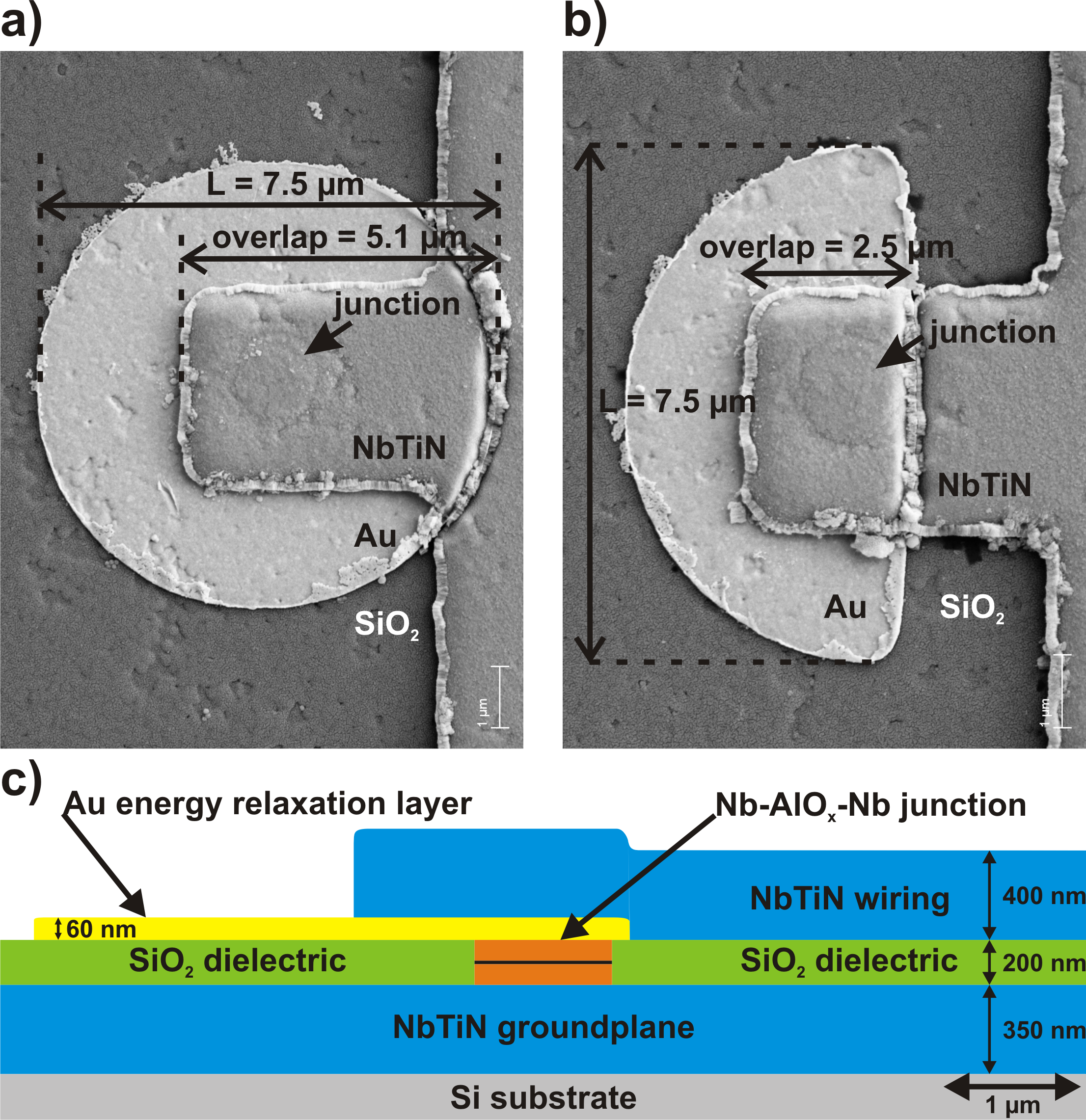
With these findings one would in principle favor, first, an Au layer shape with a small overlap with the NbTiN embedding circuit and, second, an Au layer with a minimum volume. A shape with these properties is e.g. a half circular shape (compare with Fig. 1).
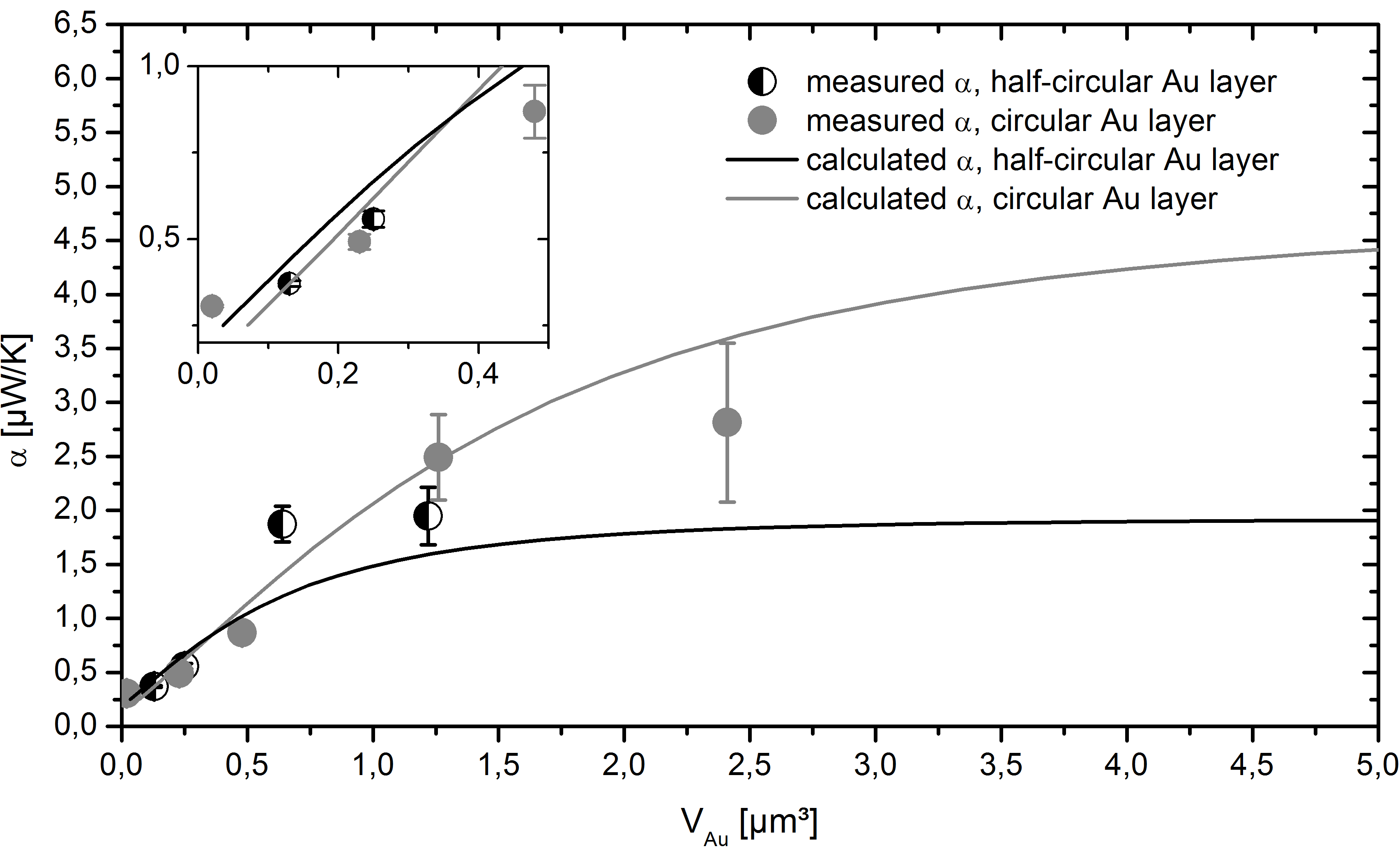
In this article we present our ongoing work and focus in particular on a thorough systematic study of the relaxation of nonequilibrium quasiparticles in various circular and half-circular shaped Au layers, added between the Nb junction and the NbTiN embedding circuit. Earlier work [9] showed a linear dependence between the volume of the Au layer and the heat-transfer coefficient alpha. On further increasing the volume of the Au-layer while keeping its thickness fixed to nm, we find in dc-measurements of the I-V characteristic a saturation in the nonequilibrium quasiparticle relaxation. This suggests an effect of the geometry on the relaxation process and we supplement our earlier findings by this new result.
We reproduced our experimental results with a simple theoretical model of our device. With this model we can also consistently describe the difference in the heating of the Nb electron gas of a device which we immersed in liquid helium (LHe) and which was characterized in a vacuum dewar. With this stage of consistency in our description, this allows us to determine the optimal Nb mixer device consisting of a full superconducting NbTiN embedding circuit and an Au energy relaxation layer.
II Energy Relaxation and Heat balance equation
Considering only lowest order tunneling processes, the quasiparticle current through a symmetric SIS junction is given by
| (1) |
with the bias voltage applied to the junction, the Fermi-Dirac distribution function of quasiparticles of energy having an effective electron temperature and the quantities are the normalized BCS density of states of the electrodes [10]. The normal-state resistance of the tunnel junction, , is a measure for the transmissivity of the tunnel barrier. In order to provide a large RF bandwidth of a SIS mixer, one prefers low products, or high current densities, where is the area of the tunnel junction [3]. By using Eq. (1) one assumes that the tunnel current does not disturb the physical properties of the two junction electrodes. Hence, one uses the Fermi-Dirac distribution at the electron temperature and the value for at the same temperature. In equilibrium, is equal to the phonon bath temperature .
For a quasiparticle nonequilibrium distribution due to dissipated power in the SIS junction, . This elevated directly influences the Fermi-Dirac distribution and consequently the superconducting energy gap through the self-consistency relation [10]
| (2) |
where is the single-spin density of states at the Fermi energy in the normal state, is the Boltzmann constant, is the Debye temperature of the material, is the average attractive interaction potential of superconductivity describing phonon exchange between electrons [10] and is the independent quasiparticle energy measured relative to the Fermi energy. The temperature depends on the power generated by the tunneling process. The power rapidly rises for bias voltages . In case that this increases , Eq. (2) implies that the relevant energy gap for the tunneling decreases leading to the possibility of back-bending [6, 8, 9] (the slope of becomes negative around ). Therefore, the slope of directly probes over the reduction in . In order to deal with non-idealities in the sharpness of the I-V curve compared to the ideal situation described by Eq. (1), a phenomenological broadening parameter is introduced into the expression for allowing to estimate the smearing of around due to quasiparticle energy broadening [11, 8], e.g. caused by an external magnetic field which we use to suppress the Josephson effect during our measurements. This magnetic field also closes the small mini-gap in the Au-layer that developes due to the proximity effect.
The actual value of depends on the energy relaxation channels in the device. The injection of hot electrons by the tunnel barrier into the junction electrodes is followed by the fast electron-electron relaxation with characteristic time . This process is usually fast enough so that one can assume a homogeneous effective electron temperature . In a closed volume where diffusion processes play no role, is relaxed via the slower electron-phonon relaxation with characteristic time . In an open volume, like it is the case for our small Au layer, diffusion processes play a role and provide an additional relaxation channel for quasiparticles. This balancing of via the aforementioned processes is described by the following general heat-balance equation [12]
| (3) |
Its solution describes the radial temperature distribution around the SIS junction in the Au layer shown in Fig. 1. The thermal conductivity is denoted by , is the radial position, measured from the center of the SIS junction, is the heat-transfer coefficient (measured in ) to the phonon system, is the spatially dependent electron temperature in the Au layer, is the bath (phonon) temperature as before and is the thickness of the Au layer. We distinguish between the metallic phonon system, where with being the metallic electron-phonon heat-transfer coefficient and the heat transfer to the phonon bath system (substrate of LHe). In this case is with being the Kapitza conductance between the metal and the substrate or between the metal and the LHe. For our interpretation it turned out that the dominating relaxation channel (i.e. the slowest relaxation process) is given by the Kapitza resistance, so we set for further calculations.
Furthermore, for the interpretation of our experiments, we use a second linearized heat balance equation
| (4) |
Here, is an effective heat-transfer coefficient. Comparing Eq. (4) and Eq. (3), for a distributed layer of Au where quasiparticle relaxation via diffusion and electron-phonon scattering occurs simultaneously, contains both relaxation contributions. This is in contrast to the definition of we used in our earlier work [8] where was used to describe relaxation only via heat transfer to the phonon system. By calculating from Eq. (3), the effective can be determined by using Eq. (4). This provides a way for direct comparison with experiments since we determine the effective experimentally over a measurement of at voltages around from which we obtain . Finally, by inverting Eq. (2) we obtain and similarly . More details are described in [8, 9].
In order to describe our device geometries, i.e. in particular the circular and half-circular shaped Au layers, Eq. (3) has to be supplemented by sufficient boundary conditions. These read
| (5) |
and
| (6) |
The boundary condition in Eq. (5) describes the power dissipation in the SIS junction of radius and subsequent inflow of heat into a circular shaped Au layer when the factor of ”2” is used and otherwise inflow of heat into the half-circular shaped Au layer. Equation (6) ensures continuity of the solution at the boundary of the Au layer with radius (compare with Fig. 1). Furthermore, is the thickness of the Au layer and is the area of the SIS junction which is 1 in our experiments.
III Experiment and Measurement Results
We have fabricated Nb-Al--Nb SIS tunnel junctions embedded in a NbTiN-SiO2-NbTiN circuit with an Au energy relaxation layer between the junction and the top NbTiN layer. We varied the size of the Au layer for a fixed thickness of nm and realized circular and half-circular shapes like shown in Fig. 1. For this paper we performed two measurements with these devices, briefly described below. In measurement #1 we obtained I-V curves of a large number of devices in a dipstick setup, where the devices were immersed in LHe. A weak magnetic field was used to suppress the Josephson effect in order to obtain only the quasiparticle current . We obtained the electron temperature as a function of dissipated power from our experimental data and extracted via Eq. (4). In Fig. 2 we have plotted the measured as a function of Au volume. In order to compare our results with theory we use the framework described in Sec. II. We solved Eq. (3) while keeping the Au thickness nm fixed and varied the radius of the Au layer in order to increase its volume . This volume is shown on the x-axis of Fig. 2. The effective heat-transfer coefficient is obtained by evaluating in Eq. (3) using , [13] as a function of dissipated power . The result for is substituted in Eq. (4) and after this solved for . In our earlier work [8] we included a conservative correction term of to the calculated in order to account for quasiparticle energy broadening . In this work we increased it to which leads to a better agreement with our measured data. This modification is reasonable because small changes in e.g. the magnetic field used to suppress the Josephson effect in our devices might very well lead to this slight change in the quasiparticle energy broadening correction. Furthermore, we added an offset to the calculated equal to the heat-transfer coefficient of the Nb junction alone. Our theoretical results are shown as lines in Fig. 2 and are in good agreement with the measured data shown as points. We could also reproduce this result by increasing the values for and both at the same time by 30 % but keeping the energy broadening correction term at . This could be attributed to possible changes in our Au film parameters which were not remeasured for this work. Because our fabrication process is in general very stable the modification of the energy broadening correction term is more reasonable. For our measured data as well as for the theoretical prediction we find a saturation in when we increase the volume by increasing only . On the other hand, when the volume is increased by increasing and possibly also , increases as well. This result is crucially important for the design of Au energy relaxation layers since we find that increasing is limited by the value .
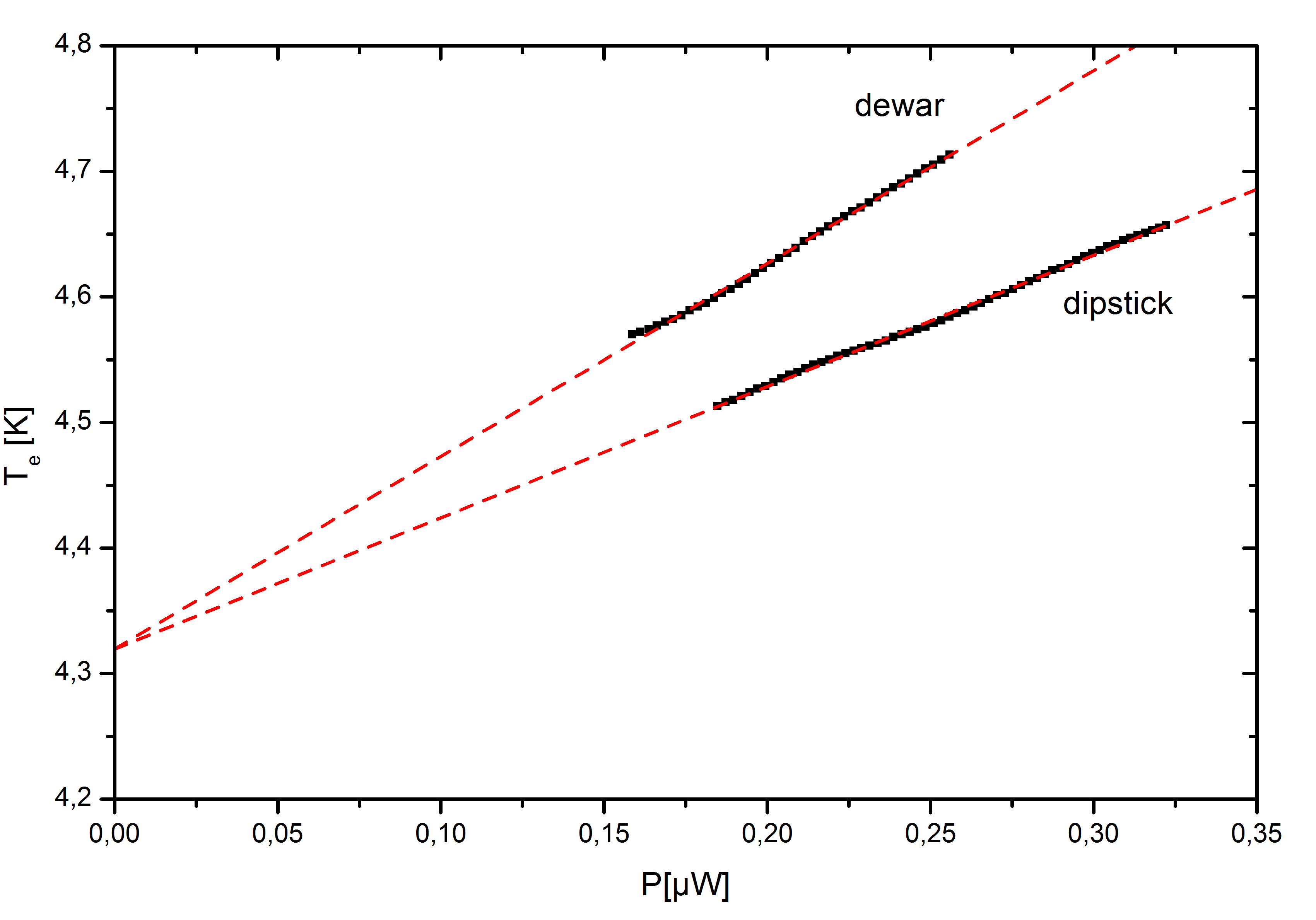
In measurement #2 we measured the I-V characteristic of a device mounted in a vacuum dewar, like it would be used in an astronomical receiver. In this case the significantly smaller Kapitza conductance between Au and results in a stronger heating effect than one would obtain for the same measurement with the device immersed in a LHe vessel where the Kapitza conductance is three times larger (values for the Kapitza resistances we used can be found in [14, 13]). In Fig. 3 we show measurements of the effective electron temperature as a function of dissipated power in a device measured in the vacuum dewar and when it is directly immersed in LHe. We adjusted to approximately in the LHe vessel for better comparison since this was the bath temperature in the vacuum dewar. The dimensions of the circular Au layer in the device are m and . Within the framework presented in Sec. II, we can consistently describe both measurements for the effective electron temperature against dissipated power . In order to relax towards and when the device is operated in the vacuum dewar, the volume of the Au energy relaxation layer has to be significantly increased due to the much smaller Kapitza conductance compared to the larger Kapitza conductance in LHe. Using our theoretical model, we find that the Au cap should then have the dimensions m and () for which our model yields an effective heat-transfer coefficient of .
Like described before, a device with a half-circular Au layer has practical advantages over a circular Au layer. Hence, translating our measurement results performed in the vacuum dewar for the device with the circular shaped Au layer to a device having only a half-cicular Au layer, this device should have m and a larger thickness () in order to reach with the same .
IV Conclusion
In our previous measurements, we found no clear evidence of a geometrical influence of the Au layer on the relaxation of nonequilibrium quasiparticles [9]. This is due to the fact that we performed our measurements in the linear regime, shown in Fig. 2 for small volumes . Hence our conclusion was that the relaxation of nonequilibrium quasiparticles does not depend on the geometry but only on the volume of the Au layer. While this is true for the linear regime of Eq. (3), in this work we find that this conclusion does not hold in the nonlinear regime. For the device in a vacuum dewar, in order to relax towards we find that for a circular Au layer a volume of only is needed while for a half-circular Au layer an approximately twice as large volume of is needed. Hence, we have determined the optimum dimensions of an either circular or half-circular Au energy relaxation layer to maintain a bath temperature quasiparticle distribution in the Nb junction when it is connected to a full superconducting NbTiN embedding circuit.
In the next development step we will use our findings to fabricate SIS mixer devices for 800 GHz to show if the nonequilibrium quasiparticle distribution in the junction can be eliminated by the Au energy relaxation layer in the same way when the device is irradiated with a strong RF signal. If this is successful we will continue this development towards a SIS mixer for 1.1 THz.
Acknowledgments
This work is carried out within the Collaborative Research Council 956, subproject D3, funded by the Deutsche Forschungsgemeinschaft (DFG) and by BMBF, Verbundforschung Astronomie under contractno. 05A08PK2. The devices were fabricated in the KOSMA microfabrication laboratory and measured at the I. Physikalisches Institut, Universität zu Köln. We thank R. Bruker from the Institut für Physikalische Chemie of the Universität zu Köln for the SEM images.
References
- [1] Th. de Graauw et al., “The Herschel-Heterodyne Instrument for the Far-Infrared (HIFI),” Astron. Astrophys., vol. 518, p. L6, 2010.
- [2] J. Zmuidzinas and P. L. Richards, “Superconducting Detectors and Mixers for Millimeter and Submillimeter Astrophysics,” Proc. IEEE, vol. 92, p. 1597, 2004.
- [3] J. R. Tucker and M. J. Feldman, “Quantum detection at millimeter wavelengths,” Rev. Mod. Phys., vol. 57, p. 1055, 1985.
- [4] B. D. Jackson et al., “Low-noise 0.8-0.96- and 0.96-1.12-THz superconductor-insulator-superconductor mixers for the Herschel Space Observatory,” IEEE Trans. Microw. Theory Techn., vol. 54, no. 2, p. 547, 2006.
- [5] M. Kroug et al., “SIS Mixer Fabrication for ALMA Band10,” IEEE Trans. Appl. Supercond., vol. 19, no. 3, p. 171, 2009.
- [6] B. Leone et al., “Geometric heat trapping in niobium superconductor-insulator-superconductor mixers due to niobium titanium nitride leads,” Appl. Phys. Lett., vol. 76, no. 6, p. 780, 2000.
- [7] B. D. Jackson et al., “Niobium titanium nitride based superconductor-insulator-superconductor mixers for low-noise terahertz receivers,” J. Appl. Phys., vol. 97, no. 11, p. 113904, 2005.
- [8] M. P. Westig et al., “Improved Nb SIS devices for heterodyne mixers between 700 GHz and 1.3 THz with NbTiN transmission lines using a normal metal energy relaxation layer,” J. Appl. Phys., vol. 114, p. 124504, 2013.
- [9] S. Selig et al., “Different shape normal metal interlayers between niobium based SIS junctions and niobium titanium nitride leads and their influence on the electron temperature,” J. Phys.: Conf. Ser., vol. 507, p. 042039, 2014.
- [10] J. Bardeen, L. N. Cooper and J. R. Schrieffer, “Theory of Superconductivity,” Phys. Rev., vol. 108, p. 1175, 1957.
- [11] R. C. Dynes, V. Narayanamurti, and J. P. Garno, “Direct Measurement of Quasiparticle-Lifetime Broadening in a Strong-Coupled Superconductor,” Phys. Rev. Lett, vol. 41, p. 1509, 1978.
- [12] W. J. Skocpol, M. R. Beasley and M. Tinkham, “Self-heating hotspots in superconducting thin-film microbridges,” J. Appl. Phys, vol. 45, p. 4045, 1974.
- [13] R. C. Johnson and W. A. Little, “Experiments on the Kapitza Resistance,” Phys. Rev., vol. 130, p. 596, 1963.
- [14] V. E. Holt, “Thermal Resistivity at Interfaces between Metal and Dielectric Films at 1.5 to 4.2 K,” J. Appl. Phys., vol. 37, p. 798, 1966.