Surface band structure of (111)
Abstract
Theoretical and experimental studies agree that () to be a three-dimensional topological insulator. However, there is still a debate on the corresponding (111) surface band structure. While three spin polarized bands have been claimed experimentally, theoretically, only two surface bands appear, with the third band being attributed to surface imperfections. Here, we address this controversy using angle-resolved photoemission spectroscopy (ARPES) on films. To minimize surface imperfections, we have optimized the sample growth recipe. We have measured the evolution of the surface band structure of with increasing gradually from to . Our ARPES data show better agreement with the theoretical calculations, where the system is topologically non-trivial with two surface bands.
pacs:
79.60.-i, 73.20.-At, 73,21-Fg, 75.70.-TjTopological insulators (TIs) are characterized by ungapped and protected edge/surface states that render the surface metallic. These states exhibit a non-trivial topology that imposes an odd number of crossings with the Fermi level Fu et al. (2007); Hasan and Kane (2010). The first angle-resolved photoemission spectroscopy (ARPES) data showing the non-trivial topology have been measured on the (111) surface of the semiconducting phase of a single crystal for Hsieh et al. (2008). Its experimental band structure is similar to pure Bi(111) especially at the -point where two spin-polarized surface bands emerge from the bulk valence band continuum Ast and Höchst (2003); Ast and Hochst (2004); Hofmann (2006); Hsieh et al. (2008). However, the band structure around the -point is still controversial. While experimentally the topological character has been claimed by the presence of a third spin polarized band (absent in Bi(111)) and correspondingly five crossings with the Fermi level Hsieh et al. (2008, 2009); Nishide et al. (2010); Nakamura et al. (2011), theoretically the number of crossings is also odd, but the configurations of the topological surface states do not include a third surface band Teo et al. (2008); Zhang et al. (2009). This additional band has been ascribed to result from imperfect surfaces Zhang et al. (2009).
Here, we experimentally examine the above debate using ARPES on films. We optimized the in situ film growth method to minimize surface imperfections. We were able to control Sb concentration from to as Sb content is a critical parameter to determine the electronic properties of the alloy. In order to have an overall view on the surface band structure, we tracked the evolution of the surface states not only near the -point but also around the -point. The ARPES results show on one hand a gradual evolution of the surface band structure from Bi(111) towards Sb(111), attesting precise control of the Sb content. On the other hand, we show that the third surface band could not be detected in the topological regime. Still, the corresponding surface band structure remains topological in accordance with the theory.

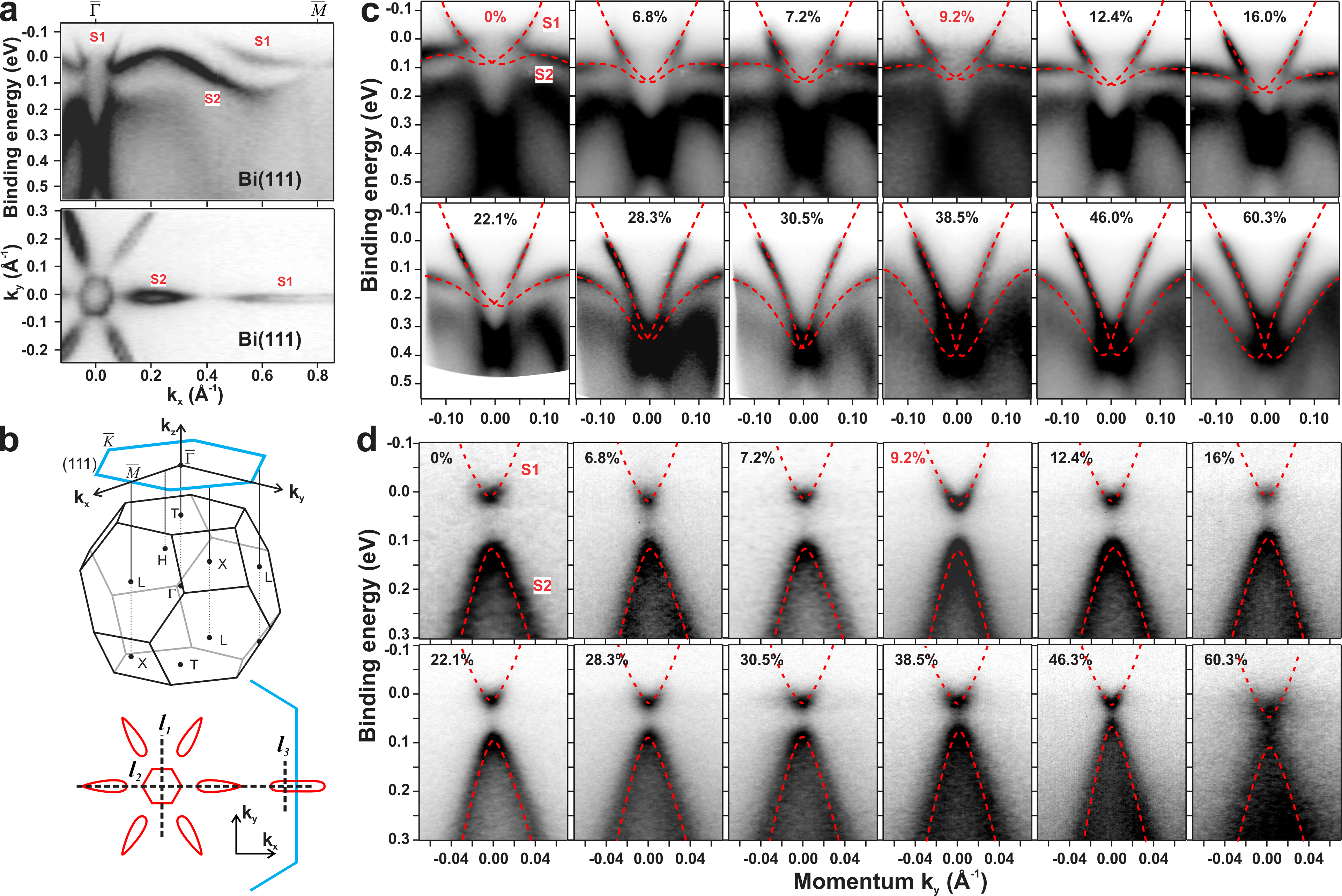
For the preparation of samples, we have adopted an optimized growth procedure that produces high quality surfaces yielding sharp experimental band structure for Sb concentrations . First, a 30 nm thick pure Bi(111) film is grown on a Si(111)-77 substrate. The sample is post-annealed at 500 K. As shown in Fig. 1-a, this growth method gives rise to a sharp and intense ARPES structure even at room temperature. On this buffer layer, we grow 120 nm thick (111) films. Bi and Sb are simultaneously deposited from Knudsen (effusion) cells. The Sb concentration has been determined from x-ray photoemission (XPS) spectra. An atomic sensitivity factor ratio has been used to find the Sb to Bi concentration ratio. The ratio was determined independently by energy dispersive x-ray spectroscopy (EDX). The ARPES measurements were performed with a hemispherical SPECS HSA3500 electron analyzer characterized by an energy resolution of about 10 meV. Monochromatized He I (21.2 eV) radiation was used as a photon source. The sample was measured either at 100 K or at room temperature to follow the dispersion of the surface states above the Fermi level.

Figure 1-c presents the experimental surface band-structure of along the line (Fig. 1-b) as Sb concentration increases progressively from to . In all panels, the surface states and appear sharp and intense. The broad features below the surface states around the -point are surface resonances appearing within the projected bulk valence band Ast and Höchst (2003); Ast and Hochst (2004); Hofmann (2006); Sugawara et al. (2006). Figure 1-c nicely shows a gradual evolution of the surface band structure near the -point going from a pure Bi(111)-like to a pure Sb(111)-like band structure. As is known from the Bi(111) surface band structure, and lose spectral weight near the -point since they disperse into the projected bulk valence band Ast and Höchst (2003); Ast and Hochst (2004); Hofmann (2006). The crossing of the spin-split bands and cannot, therefore, be discerned. The red dashed lines crossing at the -point in Fig. 1-c are an extrapolation of the experimental dispersion of and based on a theoretically calculated band structure of Bi(111) Koroteev et al. (2004).
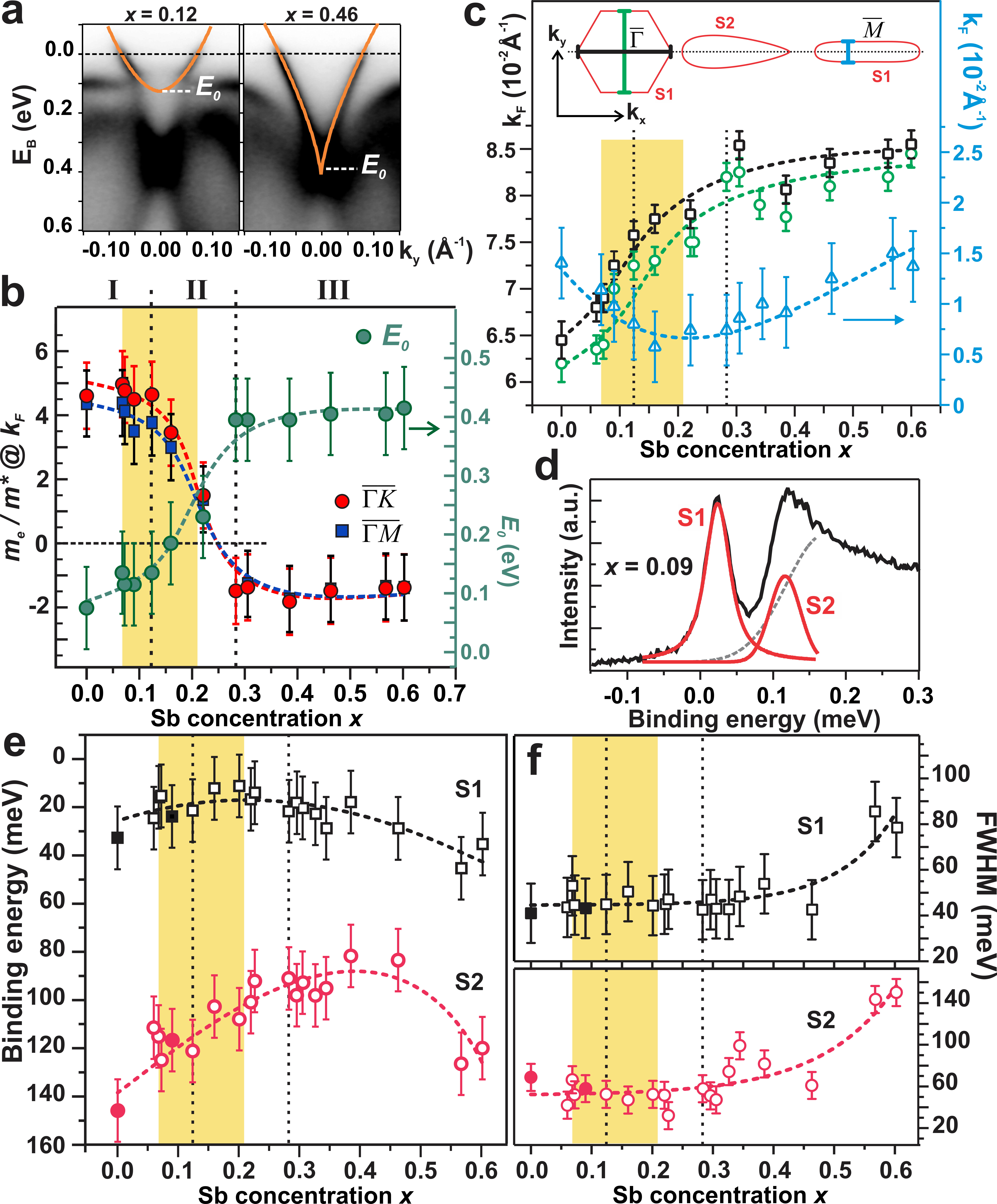
The surface band structure of Bi(111) in Fig. 1-c remains almost unchanged when increasing from to . For , a deformation of the dispersion occurs: The effective mass of changes sign at . In order to analyze the evolution of of as a function of Sb concentration, we fitted its dispersion with a symmetric power function. Figure 2-a presents different fits to at two different concentrations. The fit details are summarized in the supplemental material Epaps . In Fig. 2-b, we plot the extracted evolution of at the Fermi level. Three main Sb-concentration regions can be distinguished. They are denoted as regions I to III and delimited by dotted vertical lines in Fig. 2. In region I (), the anisotropy along and is due to the hexagonal warping of the electron pocket formed by Ast and Höchst (2001); Hofmann (2006). In region II (), the sign of changes, so that at , the band dispersion is linear. In this region, the transition of the dispersion of the surface states from a Bi(111)-like configuration (region I) to an Sb(111)-like configuration (region III) takes place. We attribute this change to the shifting bulk bands near the T and H points Lenoir et al. (1996); Tang and Dresselhaus (2012). While the band at the T point shifts to higher binding energy () for increasing , the band at the H point shifts towards the Fermi level (see Fig. 4).
The evolution of the experimental band structure of the surface states along the line near the -point is shown in Fig. 1-d as a function of Sb content. The bands are sharp and intense, but seem to not deviate much from the pure Bi(111) band dispersion in the entire concentration range, except at , where they become faint and washed-out. This broadening and intensity loss is not related to the surface quality of the sample, since the bands are very sharp around (Fig. 1-c). We have analyzed the energy distribution curves (EDC) at of the band structures in Fig. 1-d by fitting a Voigt function to the spectral features of the and bands (Fig. 2-d). The energy positions of and (Fig. 2-e) evolve smoothly as increases. The binding energy of varies from meV for pure Bi, goes to a minimum of meV for , then increases again and reaches meV at . Similarly, the energy position decreases slowly from meV at to a minimum meV for an Sb content of and then increases again to meV at . We note that the TI region does not constitute any special stage in the evolution of and energy positions Hsieh et al. (2008); Lenoir et al. (1996); Tang and Dresselhaus (2012); Nishide et al. (2010). In order to check for any hidden phenomena within the linewidth of the two surface bands, we analyzed the linewidth (FWHM) for each spectral feature. The extracted evolution of the linewidth for and is also smooth as shown in Fig. 2-f. The band is characterized by a smaller linewidth than , which is most likely due to a longer quasiparticle lifetime near the Fermi level. For , has a linewidth of about meV, which stays almost constant with increasing Sb content until . For , it increases comparatively rapidly to around meV at . The linewidth of follows the behavior of with constant values around meV until , after which it increases to about meV at .

We note that the linewidth of does not show any additional broadening within the TI region. This observation is different from previous ARPES results that indicate an additional broadening Hirahara et al. (2010); Nakamura et al. (2011); Nishide et al. (2010); Guo et al. (2011). Those ARPES measurements show the presence of a weak contribution to the linewidth of for , and Nishide et al. (2010); Nakamura et al. (2011); Hirahara et al. (2010); Guo et al. (2011). An extra broadening of could agree with the appearance of a third spin-polarized surface band (), which would result in five crossings with the Fermi level proving the non-trivial topology classification of the system as indicated in Ref. Hsieh et al. (2008, 2009). However, the expected energy position of is about meV from at Hsieh et al. (2008, 2009). With a linewidth of of about meV, a shoulder near the peak in the EDC curves corresponding to should be observable. Here, neither a peak nor a shoulder corresponding to could be resolved. In addition, no indication of the presence of even above the Fermi level can be seen in any of the ARPES data recorded at room temperature (see Fig. 2-e 2f and, . 3 Epaps ). On the other hand, comparing the ARPES results in which has been detected, a certain inconsistency about can be observed: A) has different dispersions along the direction in the literature Hsieh et al. (2008, 2009); Nishide et al. (2010); Nakamura et al. (2011); Hirahara et al. (2010); Guo et al. (2011). B) The reported energy separation between and at has different values ranging from to meV Hsieh et al. (2008, 2009); Nishide et al. (2010); Nakamura et al. (2011); Hirahara et al. (2010); Guo et al. (2011). Hence, in contrast to and , the detection of seems to be not easily reproducible and to be more sporadic than systematic. However, the presence of is not the ultimate proof of the non-trivial topology of the insulating BiSb alloy. Ab initio and tight-binding calculations describe the topological phase with only and Zhang et al. (2009); Teo et al. (2008). Furthermore, the observed in the experiment has not been related to the non-trivial topology but to surface imperfections Zhang et al. (2009); Nakamura et al. (2011). can originate, for example, from locally different surface terminations Zhu and Hofmann (2014). Thus, the uncontrolled damage to the surface caused by crystal cleaving can explain the sporadic character of . In this regard, the results presented here from in situ grown films with comparatively reduced surface damage are closer to the realistic representation of the topological insulator .
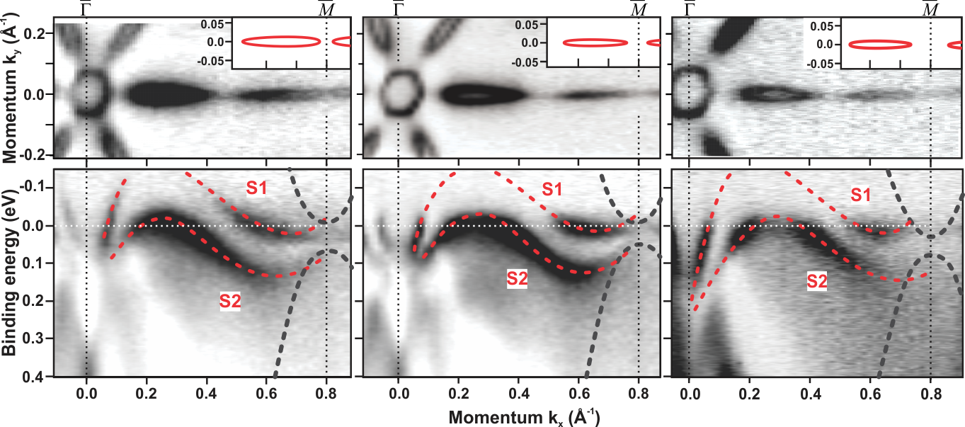
With the absence of in the non-trivial topological phase, can not hybridize with , but merges into the conduction band near the -point. The number of crossings with the Fermi level is still odd (five) Zhang et al. (2009); Nakamura et al. (2011). It ensues that the electron pocket at does not enclose the -point in the Fermi surface Zhang et al. (2009); Hsieh et al. (2008, 2009). In Fig. 3, the measured Fermi surfaces of and , which belong to the TI region are plotted. Closing electron-pockets contours just before the -point can be discerned, especially for . For , the size of the electron pocket is smaller (Fig. 2-c) preventing us from resolving its contour outline. On the corresponding experimental surface band structures along shown in the bottom panels, the intensity of and vanishes at (Fig. 3). The red dashed lines are a guide to the eye. In addition, also the experimental band structure for in Fig. 3 clearly shows a closed contour of the electron pocket and merging into the conduction band before . Consequently, the experimental surface band structure of the topologically non-trivial phase of (111) is in agreement with the theoretical modeling presented in Ref. Zhang et al., 2009.

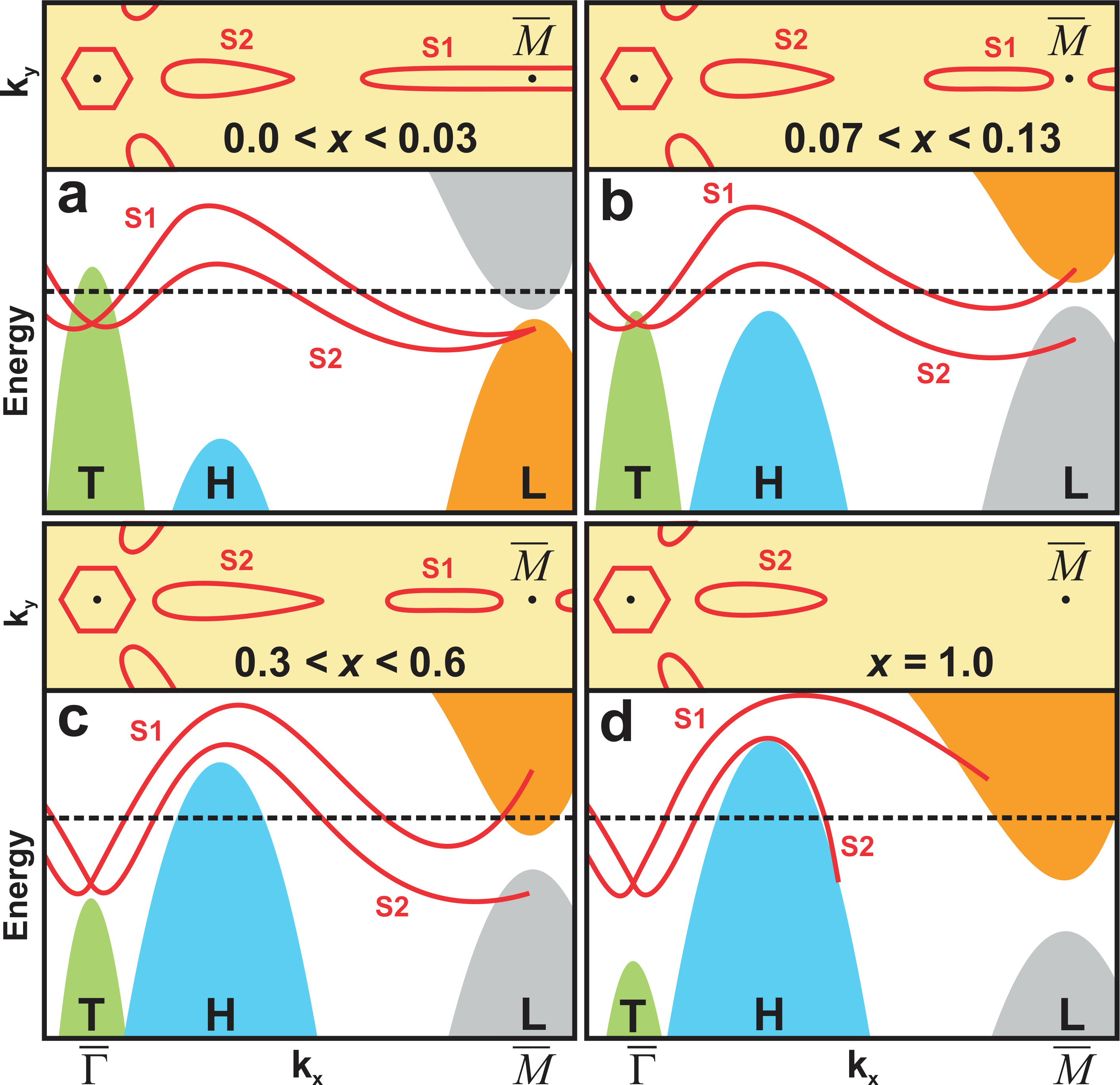
We conclude that the defect-reduced (111) surface bears only two surface states and regardless of Sb concentration . We schematically present the evolution of the surface states and as a function of Sb content in Fig. 4. For pure Bi(111) (Fig. 4-a), has been considered to connect to the valence band at NB . It switches connection from the valence band to the conduction band near at the topological transition () (Fig. 4-b). The surface state bands and further adapt to the energy shift of the bulk bands as Sb content increases. They smoothly evolve from a Bi(111)-like dispersion to the characteristic Sb(111)-like band structure (Fig. 4-c). This adaptation is most visible around within . However, it is not until that and become broad and faint near indicating convergence to the Sb(111) band structure (Fig. 4-d) Hsieh et al. (2009, 2010).
In summary, following an optimized method to grow high quality (111) films, we have investigated the evolution of the surface states of the system by a variation of from to using ARPES. Around the ARPES data show a gradual evolution of the surface band structure from Bi(111) towards Sb(111). The previously reported third surface band near could not be detected in the topologically insulating phase here. We find our results of the experimental (111) surface state band structure to agree with available theoretical predictions, which identify the crystal as topologically non-trivial with two surface states.
We acknowledge stimulating discussions with A. Schnyder. H. M. B. acknowledges funding from the Deutsche Forschungsgemeinschaft (DFG). C. R. A. acknowledges funding from the Emmy-Noether-Program of the Deutsche Forschungsgemeinschaft (DFG).
References
- Fu et al. (2007) L. Fu, C. L. Kane, and E. J. Mele, Phys. Rev. Lett. 98, 106803 (2007),
- Hasan and Kane (2010) M. Z. Hasan and C. L. Kane, Rev. Mod. Phys. 82, 3045 (2010),
- Hsieh et al. (2008) D. Hsieh, D. Qian, L. Wray, Y. Xia, Y. S. Hor, R. J. Cava, and M. Z. Hasan, Nature 452, 970 (2008),
- Ast and Höchst (2003) C. R. Ast and H. Höchst, Phys. Rev. B 67, 113102 (2003),
- Ast and Hochst (2004) C. R. Ast and H. Höchst, Phys. Rev. B 70, 245122 (2004),
- Hofmann (2006) P. Hofmann, Prog. Surf. Sci. 81, 191 (2006),
- Hsieh et al. (2009) D. Hsieh, Y. Xia, L. Wray, D. Qian, A. Pal, J. H. Dil, J. Osterwalder, F. Meier, G. Bihlmayer, C. L. Kane, et al., Science 323, 919 (2009),
- Nishide et al. (2010) A. Nishide, A. A. Taskin, Y. Takeichi, T. Okuda, A. Kakizaki, T. Hirahara, K. Nakatsuji, F. Komori, Y. Ando, and I. Matsuda, Phys. Rev. B 81, 041309 (2010),
- Nakamura et al. (2011) F. Nakamura, Y. Kousa, A. A. Taskin, Y. Takeichi, A. Nishide, A. Kakizaki, M. D’Angelo, P. Lefevre, F. Bertran, A. Taleb-Ibrahimi, et al., Phys. Rev. B 84, 235308 (2011),
- Teo et al. (2008) J. C. Y. Teo, L. Fu, and C. L. Kane, Phys. Rev. B 78, 045426 (2008),
- Zhang et al. (2009) H.-J. Zhang, C.-X. Liu, X.-L. Qi, X.-Y. Deng, X. Dai, S.-C. Zhang, and Z. Fang, Phys. Rev. B 80, 085307 (2009),
- Sugawara et al. (2006) K. Sugawara, T. Sato, S. Souma, T. Takahashi, M. Arai, and T. Sasaki, Phys. Rev. Lett. 96, 046411 (2006),
- Koroteev et al. (2004) Y. M. Koroteev, G. Bihlmayer, J. E. Gayone, E. V. Chulkov, S. Blügel, P. M. Echenique, and P. Hofmann, Phys. Rev. Lett. 93, 046403 (2004),
- (14) See Supplemental Material for fit procedure and results, additional ARPES data, examples of XPS spectra.
- Ast and Höchst (2001) C. R. Ast and H. Höchst, Phys. Rev. Lett. 87, 177602 (2001),
- Lenoir et al. (1996) B. Lenoir, M. Cassart, J.-P. Michenaud, H. Scherrer, and S. Scherrer, J. Phys. Chem. Sol. 57, 89 (1996),
- Tang and Dresselhaus (2012) S. Tang and M. S. Dresselhaus, Phys. Rev. B 86, 075436 (2012),
- Hirahara et al. (2010) T. Hirahara, Y. Sakamoto, Y. Saisyu, H. Miyazaki, S. Kimura, T. Okuda, I. Matsuda, S. Murakami, and S. Hasegawa, Phys. Rev. B 81, 165422 (2010),
- Guo et al. (2011) H. Guo, K. Sugawara, A. Takayama, S. Souma, T. Sato, N. Satoh, A. Ohnishi, M. Kitaura, M. Sasaki, Q.-K. Xue, et al., Phys. Rev. B 83, 201104 (2011),
- Zhu and Hofmann (2014) X.-G. Zhu and P. Hofmann, Phys. Rev. B 89, 125402 (2014),
- (21) Theoretical and experimental works on Bi(111) consider to connect to the valence band at Nakamura et al. (2011); Zhang et al. (2009); Koroteev et al. (2004). However, some others show that it rather connects to the conduction band Ast and Höchst (2003); Ohtsubo et al. (2013). The discussion on this issue is out of the scope of our present paper.
- Ohtsubo et al. (2013) Y. Ohtsubo, L. Perfetti, M. O. Goerbig, P. L. Fèvre, F. Bertran, and A. Taleb-Ibrahimi, N. J. Phys. 15, 033041 (2013),
- Hsieh et al. (2010) D. Hsieh, L. Wray, D. Qian, Y. Xia, J. H. Dil, F. Meier, L. Patthey, J. Osterwalder, G. Bihlmayer, Y. S. Hor, et al., N. J. Phys. 12, 125001 (2010),