Photonic Architectures for Equilibrium High-Temperature Bose-Einstein Condensation in Dichalcogenide Monolayers
Semiconductor-microcavity polaritons are composite quasiparticles of excitons and photons, emerging in the strong coupling regime. As quantum superpositions of matter and light, polaritons have much stronger interparticle interactions compared with photons, enabling rapid equilibration and Bose-Einstein condensation (BEC). Current realizations based on 1D photonic structures, such as Fabry-Pérot microcavities, have limited light-trapping ability resulting in picosecond polariton lifetime. We demonstrate, theoretically, above-room-temperature (up to 590 K) BEC of long-lived polaritons in MoSe2 monolayers sandwiched by simple TiO2 based 3D photonic band gap (PBG) materials. The 3D PBG induces very strong coupling of 40 meV (Rabi splitting of 62 meV) for as few as three dichalcogenide monolayers. Strong light-trapping in the 3D PBG enables the long-lived polariton superfluid to be robust against fabrication-induced disorder and exciton line-broadening.
Semiconductor microcavities with engineered photonic states are a valuable platform to observe fundamental and emergent quantum electrodynamic phenomenamc . Polaritons are formed as a quantum superposition of semiconductor-excitons and microcavity-photons when the exciton-photon interaction is much larger than their decay rates. The ability to tailor the photonic modes, light-matter interaction and polariton lifetime in semiconductor microcavities enables versatile control of polaritons and opens the possibility of novel quantum effects such as Bose-Einstein condensation (BEC) at elevated temperaturesbec1 ; bec2 ; bec3 ; bec4 ; deng . Picosecond time-scale quasiequilibrium room-temperature polariton BEC has been claimed in ZnOzno ; zno2 , GaNgan ; gan2 ; gan3 , and polymerspolymer in Fabry-Pérot microcavities. This is possible when the thermalization time is even shorter than the polariton lifetime. However, for both scientific studies and applications, it is more favorable to achieve room-temperature polariton BEC with polariton lifetimes on the scale of 100 ps - 1 ns. Realization of long-lived, room-temperature, equilibrium polariton BEC remains an important target for fundamental research and practical applicationrt .
In this article, we demonstrate theoretically a route to simultaneously achieve very strong exciton-photon coupling and long polariton lifetime using a simple TiO2 based photonic band gap (PBG)pbg ; pbg2 material sandwiching a planar quantum-well slab containing as few as three monolayers of the transition-metal dichalcogenide MoSe2shen . This architecture provides a realistic, technologically accessible route toward equilibrium polariton BEC above room temperature. In contrast, the corresponding Fabry-Pérot microcavity has picosecond polariton lifetime due to radiative recombination into unwanted leaky (air) modes that are degenerate with the microcavity mode. These leaky modes couple strongly to any finite area polariton condensate in the quantum-well region. They are eliminated by replacing the 1D periodic structure with a 3D PBG material. Recently WSe2 and MoS2 monolayers in 2D photonic crystals have been experimentally realized2dphc1 ; 2dphc2 . However, a complete 3D PBG is absent in those cavities and radiative decay of polaritons is not suppressed effectively. Another realization of a MoS2 monolayer in a Fabry-Pérot microcavitymos2-fp reveals exciton-photon coupling of 31.5 meV but very rapid (sub-picosecond) polariton decay and significant line-broadening of 38.5 meV.
In a MoSe2 monolayer the exciton binding energy is as large as 0.55 eV and the exciton Bohr radius is as small as 1.2 nmshen ; mose2 . Theoretical calculationshen predicts that 6% of incident light is absorbed during transmission through a MoSe2 layershen , indicating very strong light-matter interaction. As we show, this enables high-temperature BEC with only three quantum-well monolayers of MoSe2. Previous considerations of high-temperature, equilibrium BEC have involved on the order of 100 quantum-wellscdte . Another special property of MoSe2 is that due to correlation between wave-vector valley and spin polarizations at the electronic band edge of MoSe2, left- and right-circularly polarized light are coupled to different exciton spin and valley statesyao . In other words, optical, valley, and spin polarizations are correlated with each other. Information encoded in the spin and valley channels of the condensate can be uncovered by measuring the polarization of emitted light. This may provide a new degree of freedom to store and manipulate coherent quantum information in the predicted polariton condensateelectric ; gating ; gating2 .
Optical Microcavity Architectures
A fundamental challenge to the realization of above-room-temperature BEC is the accurate fabrication of complex photonic nanostructures. Almost all previous experimental studies have focused on 1D dielectric multi-layers which provide strong exciton-photon coupling at the expense of concomitant strong coupling to low-quality-factor leaky modes that render picosecond time-scale polariton lifetimes. 3D PBG materials enable very strong coupling without the occurrence of leaky modes. However, structures made of CdTecdte require a very large number of embedded quantum wells in the active region to provide sufficiently strong coupling to approach room temperature BEC. Here, we propose a simple route to above-room-temperature BEC using TiO2-based photonic crystal architectures. As a reference, we provide comparison with a corresponding TiO2-SiO2 1D multi-layer photonic cavity.
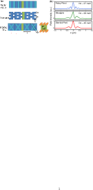
In Fig. 1 we depict the Fabry-Pérot (FP), woodpile photonic crystal (PC) and slanted-pore (SP) PC microcavities, as well as their cavity-mode field intensities along the growth -direction. There are 3 MoSe2 monolayers in the middle of each microcavity separated by 7 nm TiO2 layers (SiO2 for the FP). Inter-layer Coulomb correlation energy is suppressed due to the large static dielectric constant () of TiO2 at room temperaturehigh-d . The Coulomb interaction energy for two electrons (holes) separated by 7 nm with such high dielectric constant is 2 meV, which is much smaller than other energy scales such as the exciton-photon coupling meV. Consequently, we treat excitons in each monolayer as independent. The structures of 3 microcavities are illustrated in Fig. 1a. In the woodpile PC, the height of each rod is and the width is where nm is the periodicity in the - plane (see Fig. 1a). The SP PC cavity is a SP2 structure of the familyovi with the periodicity along the direction of where nm is the in-plane lattice constant. The diameter of each cylindrical air pore is . For both types of PC microcavity, the thickness of the slab is 0.05. The SiO2-TiO2 FP cavity has two Bragg mirrors with periodicity of nm and a half-wave SiO2 slab of thickness nm in the middle, such that the lowest band edge cavity mode is close to the exciton recombination energy of 1.55 eV.
Sandwiched PC–quantum-well–PC structuresyang1 ; yang2 are fabricated in a layer-by-layer processnoda ; noda6 . The PCs and the quantum-well structure are fabricated independently, the quantum-well structure is then fused onto the lower PC and finally the upper PC is fused onto the quantum-well structurenoda ; noda6 . Corresponding technologies for TiO2 PC growth have become mature in the last decadenoda1 ; epitaxial ; ALD ; martin ; martin2 . In addition, high quality MoSe2 thin films can be grown by molecular beam epitaxyshen and chemical vapor depositioncvd .
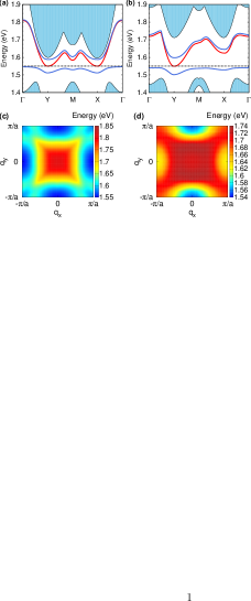
The 3D PBG’s in the woodpile and the SP PC’s are and 14%, respectively ( and are the bandwidth and the central frequency of the PBG, respectively). Photonic band structures near the 3D-PBG for the woodpile and SP PC cavities reveal several confined 2D guided bands in the PBG, among which only the lowest one (depicted in Fig. 2) is relevant for polariton BECcdte .
Strong exciton-photon coupling
The Hamiltonian of the coupled exciton-photon system can be written ascdte
| (1a) | |||
| (1b) | |||
where creates an exciton in the -th monolayer with total angular momentum along direction. The energy of the -exciton is where eV and are exciton emission energy and effective mass, respectively. In this optical transition from valence to conduction band, the electron spin is preserved but its orbital angular momentum changes by . creates a photon with wave-vector and frequency in the lowest guided 2D photonic band. The exciton-photon coupling is
| (2) |
where Cm (Supplementary Information) is the absolute value of the interband dipole matrix element, is the exciton wavefunction of the -excitonic state at zero electron-hole distance, is the vacuum permittivity, is the area of the unit cell of PC in the - plane, is the coordinate of the -th MoSe2 monolayer plane. where is the polarization vector of the exciton state with and is the periodic part of the photonic electric field . Here is the area of the system, with and . The special electronic band structure (see Fig. 3a) leads to optical selection rules for the lowest excitonic transitions: the photon excites only spin-up hole and spin-down electron in the valley, while photon excites only spin-down hole and spin-up electron in the valleyheli1 ; heli2 ; yao . Here is the total angular momentum along direction.
The resulting dispersion of the lower polariton branch is
| (3) |
Here the collective exciton-photon couplingcdte is given by . Strong light trapping leads to exciton-photon interaction as large as 40 meV and 38 meV in the SP PC and woodpile PC microcavities, respectively.
Above Room Temperature Polariton BEC
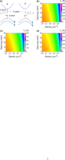
The polariton BEC transition temperature, , is calculated by the criteriononsager where and are the population on the ground state and the total polariton number respectivelyonsager . We consider a quantum box trap for polaritons with box area defined by the finite area of embedded MoSe2 thin films. As shown below, the trap size, characterized by the side length of the square box, does not alter the transition temperature considerably over a range from a few microns to one centimeter. The quantum box confinement leads to quantization of wave-vector and energy. At thermal equilibrium, , , where is the ground state energy, runs over all discrete energy levels, and is the chemical potential. As shown previouslycdte , is essentially defined by the polariton dispersion depth, , where is the exciton-photon detuning and is the exciton-photon coupling at photonic band edge. As approaches , the population on exciton-like states with very large effective mass becomes significantcdte . The pure exciton BEC transition temperature is calculated to be less than K for density less than and trap size of 1 micron in a MoSe2 monolayer. On the other hand for positive detuning meV and meV, the dispersion depth is 58 meV. This can support polariton BEC up to K.
Figs. 3(b)-(d) give the polariton BEC transition temperatures for different detuning and polariton densities for the SP PC, woodpile PC, and FP cavities. We assume that the exciton gas is initially created by incoherent pumping that (after thermal relaxation) equally populates all degenerate dispersion minima (-points) in the photonic band structure. As seen in Fig. 2, the woodpile PC has a doubly degenerate polariton minimum whereas the polariton ground state is nondegenerate for the SP PC. The trap size is m. The is enhanced with increasing detuning as the polariton dispersion depth increases. The highest is reached at the largest detuning meV which is 590 K, 450 K, and 430 K for the SP PC, woodpile PC and FP cavities, respectively. The BEC transition temperature is highest in the SP PC cavity since it contains a nondegenerate polariton ground state. This is provided by the placement of the active layer at a plane that breaks the - symmetry of the criss-crossing pores above and below (see Fig. 1a). In contrast, there are two degenerate polariton minima in the woodpile that reduces effective polariton density for BEC by a factor of two. In the case of the FP cavity, the polariton density available for BEC is divided by the two degenerate optical polarization states at . We do not consider larger detuning because a too large will reduce the exciton fraction of polariton as well as the polariton-phonon and polariton-polartion scattering, which leads to much longer equilibration time.
The polariton BEC transition temperatures at meV for different trap sizes and polariton densities for each cavity are shown in Fig. 4. The trap size dependence is prominent for low polariton densities, but very weak for high polariton densitiescdte . At low densities, and polariton equilibrium is governed by the low-lying excited states of very small effective mass particles in the box trap that are very sensitive to . At high polariton densities, and a significant fraction of polaritons acquire the bare exciton mass for which the level spacing is less sensitive to . Eventually tends to zero for very large trap size (when the low-lying excited states are extremely close to the ground state) according to the Mermin-Wagner theoremwagner . In all these calculations the largest polariton density, m-2, corresponds to an exciton density in each MoSe2 monolayer less than , well below the exciton saturation density of saturation .

Fabrication induced disorder and exciton line broadening tend to degrade high-temperature polariton BEC. In a PBG material, light in the cavity mode is well-protected from scattering into unwanted modes. Consequently, the role of disorder is primarily to shift the cavity resonance frequency. For photonic (dielectric) disorder, our calculation indicates that in the woodpile and SP PC cavities, photonic structure deviations less than 6 nm in the active slab layer, less than 12 nm in the logs close to the active slab layer, or less than 20 nm in the logs two periods away, do not affect the band edge of the lowest planar guided mode by more than 2%. This fluctuation is equivalent to alteration of the detuning by 30 meV, which can reduce the to 360 K (480 K) if the detuning decreases to 10 meV for the woodpile (SP) PC cavity. Polariton BEC is also found to be robust to exciton homogeneous and inhomogeneous broadening although the Rabi-splitting and polariton dispersion depth are slightly reduced (e.g., Rabi splitting in SP cavity is reduced from 80 meV to 62 meV) (see Supplementary Information).
In contrast there is no 3D PBG for the FP cavity and light-trapping is not robust to disorder. Excitons in the FP with wave-vector with are strongly coupled to leaky (air) modes, leading to rapid radiative decayTassone . This decay into leaky modes is not alleviated by increasing the quality of the FP cavity mode and is exacerbated by imperfect fabrication accuracy. In real FP cavities, dielectric disorder scatters polaritons with wave-vector into leaky modes with the same energy. Such scattering significantly limits the quality factor of the (nonleaky) cavity mode (). The overall polariton lifetime due to radiative decay is very short ( ps) in SiO2/TiO2 multilayerstio2-fp and in otherzno2 FP cavities. The resulting sub-picosecond polariton lifetime (see also calculation in the Supplementary Information) is still comparable with the thermalization time, although calculations have shown that phonon scattering is very efficient (about 0.1 ps scattering time) in MoSe2 at room temperaturemose2-phonon . In contrast, PC cavities protected by a 3D PBG enable light-trapping in all directions, leading to polaritons with lifetime limited only by nonradiative decay (see Supplementary Information). This nonradiative decay is further suppressed by our detuning () that renders our polariton more photon-like than exciton-like. The quantum coherence of polaritons in the cavity can be probed and manipulated using light propagating through engineered waveguide channels in the 3D PBG claddingoc ; noda6 .
In the absence of any microcavity, optically excited valley polarization of excitons can last only about 9 ps in MoSe2 at room temperaturetau-x . In high-quality PC microcavities strong light trapping over all directions can enhance polariton lifetime beyond 130 ps (the exciton lifetime in MoSe2 monolayer without any cavity at room temperature)tau-x . When the polaritons form a BEC, optical, valley, and spin polarization coherences maintained on such long time-scales may be useful for quantum information processing based on manipulation of the spin and valley degrees of freedomgating ; gating2 .
Conclusions
We have theoretically demonstrated photonic crystal architectures based on TiO2 with very strong light-matter interaction and long polariton lifetime for above-room-temperature, equilibrium exciton-polariton BEC. The 3D photonic band gap robustly supports strongly confined guided modes in a slab cavity containing three separated excitonic MoSe2 monolayers. Unlike 1D periodic Fabry-Pérot structures that suffer from substantial radiative decay through directions other than the stacking direction, the 3D PBG structures suppress radiative decay in all directions enabling equilibration and long-time polariton coherence. An important feature of the slanted pore PC architecture is that it provides a non-degenerate lower polariton dispersion minimum, without recourse to a symmetry-breaking external fieldelectric . This enables a remarkable equilibrium high-temperature Bose-Einstein condensate, above 500 K, with only three quantum well layers. Both TiO2 based photonic crystals and MoSe2 thin films have been fabricated with mature technologies providing a very accessible route to high-temperature BEC. This BEC is robust to disorder, fabrication imperfections, exciton homogeneous and inhomogeneous line-broadening. The unique coupling among the optical, valley, and spin degrees of freedom in MoSe2 provides a condensate with novel internal symmetries that can be manipulated by external fields. Polariton BEC with long-lived optical, valley, and spin coherence persisting above room-temperature offers new opportunities for macroscopic quantum physics.
Methods
The photonic band structures and electric field distributions for PC microcavities are calculated using the plane wave expansion method, while those for the FP microcavity are calculated using the transfer matrix method. The refractive indices of TiO2 and SiO2 are 2.7 and 1.5, respectivelymaterial . In MoSe2 the effective mass for conduction band electron and valence band hole are, and , respectivelyx2 . The effective mass of exciton is . The exciton Bohr radius and interband band dipole matrix element are obtained from existing studies on electronic band structure in MoSe2 and excitonic optical absorptionshen ; yao (see Supplementary Information). The calculation of involves summation over numerous polariton states which is broken into two parts: the summation over the first 1600 states and the integration over other higher states. Polariton energy in a square (hard-wall) quantum box is calculated according to wave-vector quantization.
References
- (1) Yamamoto, Y., Tassone, T. & Cao, H. Semiconductor cavity quantum electrodynamics. (Springer, Berlin, 2000).
- (2) Deng, H., Weihs, G., Santori, C., Bloch, J., & Yamamoto, Y. Condensation of semiconductor microcavity exciton polaritons. Science 298, 199-202 (2002).
- (3) Kasprzak, J. et al. Bose-Einstein condensation of exciton polaritons. Nature 443, 409-414 (2006).
- (4) Balili, R., Hartwell, V., Snoke, D., Pfeiffer, L., West, K. Bose-Einstein condensation of microcavity polaritons in a trap. Science 316, 1007-1010 (2007).
- (5) Kasprzak, J., Solnyshkov, D. D., André, R., Dang, L. S. & Malpuech, G. Formation of an exciton polariton condensate: thermodynamic versus kinetic regimes. Phys. Rev. Lett. 101, 146404 (2008).
- (6) Deng, H., Haug, H. & Yamamoto, Y. Exciton-polariton Bose-Einstein condensation. Rev. Mod. Phys. 82, 1489-1537 (2010).
- (7) Lai, Y.-Y., Lan, Y.-P. & Lu, T.-C. Strong light-matter interaction in ZnO microcavities. Light Sci. Appl. 2, e76 (2013).
- (8) Li, F. et al. From excitonic to photonic polariton condensate in a ZnO-based microcavity. Phys. Rev. Lett. 110, 196406 (2013).
- (9) Christopoulos, S. et al. Room-temperature polariton lasing in semiconductor microcavities. Phys. Rev. Lett. 98, 126405 (2007).
- (10) Christmann, G., Butté, R., Feltin, E., Carlin, J.-F. & Grandjean, N. Room temperature polariton lasing in a GaN/AlGaN multiple quantum well microcavity. Appl. Phys. Lett. 93, 051102 (2008).
- (11) Levrat, J. et al. Condensation phase diagram of cavity polaritons in GaN-based microcavities: experiment and theory. Phys. Rev. B 81, 125305 (2010).
- (12) Plumhof, J. D., Stöferle, T., Mai, L., Scherf, U. & Mahrt, R. F. Room-temperature Bose-Einstein condensation of cavity exciton-polaritons in a polymer. Nat. Mater. 13, 247-252 (2014).
- (13) Snoke, D. Microcavity polaritons: a new type of light switch. Nat. Nanotechnol. 8, 393-395 (2013).
- (14) John, S. Strong localization of photons in certain disordered dielectric superlattices. Phys. Rev. Lett. 58, 2486-2489 (1987).
- (15) Yablonovitch, E. Inhibited spontaneous emission in solid-state physics and electronics. Phys. Rev. Lett. 58, 2059-2062 (1987).
- (16) Ugeda, M. M. et al. Observation of giant bandgap renormalization and excitonic effects in a monolayer transition metal dichalcogenide semiconductor. arXiv:1404.2331, Nat. Mater. in press.
- (17) Gan, X. et al. Controlling the spontaneous emission rate of monolayer MoS2 in a photonic crystal nanocavity. Appl. Phys. Lett. 103, 181119 (2013).
- (18) Wu, S. et al. Control of two-dimensional excitonic light emission via photonic crystal. 2D Mater. 1, 011001 (2014).
- (19) Liu, X. et al. Strong light-matter coupling in two-dimensional atomic crystals. arXiv:1406.4826
- (20) Ross, J. S. et al. Electrical control of neutral and charged excitons in a monolayer semiconductor. Nat. Commun. 4, 1474 (2013).
- (21) Jiang, J. H. & John, S. Photonic crystal architecture for room temperature equilibrium Bose-Einstein condensation of exciton-polaritons. Phys. Rev. X 4, 031025 (2014).
- (22) Xiao, D., Liu, G.-B., Feng, W., Xu, X. & Yao, W. Coupled spin and valley physics in monolayers of MoS2 and other group-VI dichalcogenides. Phys. Rev. Lett. 108, 196802 (2012).
- (23) Schneider, C. et al. An electrically pumped polariton laser. Nature 497, 348-352 (2013)
- (24) Amo, A. et al. Exciton-polariton spin switches. Nature Photon. 4, 361-366 (2010)
- (25) Cerna, R. et al. Ultrafast tristable spin memory of a coherent polariton gas. Nat. Commun. 4, 2008 (2013).
- (26) Parker, R. A. Static dielectric constant of rutile (TiO2), 1.6-1060 K. Phys. Rev. 124, 1719-1722 (1961).
- (27) Toader, O., Berciu, M., & John, S. Photonic band gaps based on tetragonal lattices of slanted pores. Phys. Rev. Lett. 90, 233901 (2003).
- (28) John, S. & Yang, S. Electromagnetically induced exciton mobility in a photonic band gap. Phys. Rev. Lett. 99, 046801 (2007).
- (29) Yang, S. & John, S. Exciton dressing and capture by a photonic band edge. Phys. Rev. B 75, 235332 (2007).
- (30) Ogawa, S., Imada, M., Yoshimoto, S., Okano, M., & Noda, S. Control of light emission by 3D photonic crystals. Science 305, 227-229 (2004)
- (31) Noda, S., Fujita, M., & Asano, T. Spontaneous-emission control by photonic crystals and nanocavities. Nature Photon. 1, 449-458 (2007).
- (32) Noda, S., Tomoda, K., Yamamoto, N. & Chutinan, A. Full three-dimensional photonic bandgap crystals at near-infrared wavelengths. Science 289, 604-606 (2000).
- (33) Nelson, E. et al. Epitaxial growth of three-dimensionally architecture optoelectronic devices. Nat. Mater. 10, 676-681 (2011).
- (34) King, J. S. et al. Infiltration and inversion of holographically defined polymer photonic crystal templates by atomic layer deposition. Adv. Mater. 18, 1561-1565 (2006).
- (35) Deubel, M., Wegener, M., Kaso, A. & John, S. Direct laser writing and characterization of “slanted-pore” photonic crystals. Appl. Phys. Lett. 85, 1895-1897 (2004).
- (36) Deubel, M. et al. Direct laser writing of three-dimensional photonic-crystal templates for telecommunications. Nat. Mater. 3, 444-447 (2004).
- (37) Shim, G. W. et al. Large-area single-layer MoSe2 and its van der Waals heterostructures. ACS Nano 8, 6655-6662 (2014).
- (38) Zeng, H., Dai, J., Yao, W., Xiao, D. & Cui, X. Valley polarization in MoS2 monolayers by optical pumping. Nat. Nanotechnol. 7, 490-493 (2012).
- (39) Mak, K. F., He, K., Shan, J. & Heinz, T. F. Control of valley polarization in monolayer MoS2 by optical helicity. Nat. Nanotechnol. 7, 494-498 (2012).
- (40) Penrose, O. & Onsager, L. Bose-Einstein condensation and liquid helium. Phys. Rev. 104, 576-584 (1956).
- (41) Mermin, N. D. & Wagner, H. Absence of Ferromagnetism or antiferromagnetism in one- or two-Dimensional isotropic Heisenberg models. Phys. Rev. Lett. 17, 1133-1136 (1966).
- (42) Schmitt-Rink, S., Chemla, D. S. & Miller, D. A. B. Theory of transient excitonic optical nonlinearities in semiconductor quantum-well structures. Phys. Rev. B 32, 6601-6609 (1985).
- (43) Savona, V. & Tassone, F. Exact Quantum Calculation of polariton dispersion in semiconductor microcavities. Solid State Commun. 95, 673-678 (1995).
- (44) Bhattacharya, P. et al. Room temperature electrically injected polariton laser. Phys. Rev. Lett. 112, 236802 (2014).
- (45) Jin, Z., Li, X., Mullen, J. T. & Kim, K. W. Intrinsic transport properties of electrons and holes in monolayer transition-metal dichalcogenides. Phys. Rev. B 90, 045422 (2014).
- (46) Chutinan, A., John, S. & Toader, O. Diffractionless flow of light in all-optical microchips. Phys. Rev. Lett. 90, 123901 (2003).
- (47) Kumar, N., He, J., He, D., Wang, Y. & Zhao, H. Valley and spin dynamics in MoSe2 two-dimensional crystals. Nanoscale, 6, 12690 (2014).
- (48) Landmann, M., Rauls, E. & Schmidt, W. G. The Electronic structure and optical response of rutile, anatase and brookite TiO2. J. Phys.: Condens. Matter 24, 195503 (2012).
- (49) Ramasubramaniam, A. Large excitonic effects in monolayers of molybdenum and tungsten dichalcogenides. Phys. Rev. B 86, 115409 (2012).
Acknowledgments
We thank J. E. Sipe, J.-L. Cheng, and R. A. Muniz for helpful discussions. This work was supported by the Natural Sciences and Engineering Research Council of Canada and the United States Department of Energy through Contract No. DE-FG02-06ER46347.
Author Contributions
J.-H.J. performed calculations and analysis. S.J. guided the research.
Additional information
Competing financial interests: The authors declare no competing financial interests.
SUPPLEMENTARY INFORMATION
Guided 2D Photonic band Edge
In the woodpile PC cavity the lowest 2D photonic band has two dispersion minima: the point and the point . The dispersion has a symmetry, inherited from the symmetry of the woodpile PC cavity. We consider the situation when the 2D photonic band edge is close to the exciton emission energy (i.e., nm) where the dispersion of the 2D photonic band near the minima is . Here, and where is the bare electron mass in vacuum. In SP PC cavity the dispersion of the lowest 2D photonic band has the symmetry. There is only one dispersion minimum at the point where the effective mass is also anisotropic with and for nm. The effective mass of photon in the FP cavity is at exciton-photon resonance.
Electronic band structure of MoSe2
Schematic of electronic band structure of MoSe2 monolayer is shown in Fig. 3a in the main text. Band extrema are located at the ( is the honeycomb lattice constant of MoSe2) and pointsyao . Very large splitting occurs between spin-up and -down states of 180 meVmose2 in the valence band due to spin-orbit interaction. Denoting the -components of total, orbital and spin angular momenta as , and , the valence band maximum at the valley gives spin-up holes (absence of an electron with and in the valence band). Its time-reversal partner valley gives spin-down holes. This special electronic band structure leads to optical selection rules for the lowest excitonic states (see Fig. 3a in the main text): the photon excites only spin-up hole and spin-down electron in the valley, while photon excites only spin-down hole and spin-up electron in the valleyyao .
Estimation of the exciton-photon coupling in MoSe2
From Ref. book the imaginary part of the optical susceptibility at the energy of the -exciton state is given by
| (4) |
where is the quantum well width and is the homogeneous broadening of the -exciton state. From measurements of we deduce .
The absorptance for an isolated two-dimensional system with thickness is
| (5) |
where and are the frequency and speed of light, respectively, and is the refractive index. From Ref. x2 the in-plane dielectric constant is 4.7 for a monolayer MoSe2. Accordingly, we choose the refractive index .
For MoSe2 the absorptance shen . It follows from Eqs. (4) and (5) that
| (6) |
From Ref. shen the homogeneous broadening at room-temperature is about 50 meV. Therefore, C which is 2.4 times as large as that of excitons GaAs quantum-wells of width 3 nm ( C). Using for the 2D exciton and the Bohr radius nmshen , we estimate Cm. This is also comparable withyao Cm where Åyao is the honeycomb lattice constant of MoSe2, eVyao is the effective electron hopping parameter, C is the electronic charge and eVshen is the electronic band gap of MoSe2.
Ultra-short polariton radiative lifetime in Fabry-Pérot microcavities
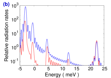
1D periodic microstructures can provide strong coupling to a single high-quality factor optical mode. However the concomitant strong coupling to degenerate leaky modes severely reduces the polariton radiative lifetime. Here, we simulate polariton radiative decay from a finite-size polariton condensate using an extended dipole at the center of a FP cavity by finite-difference-time-domain (FDTD). Different dipole sizes are used to represent small and large polariton BEC trap sizes. The radiative decay rate in the FP cavity is compared with that of the same dipole in vacuum (i.e., without the cavity). Experimentstau-x suggest that the latter is about 1/(130 ps) in a MoSe2 monolayer at room temperature. 2D FDTD simulations are used to provide a semi-quantitative prognosticator of a realistic 3D structure (see Fig. 5). The radiative decay rate (relative to that in vacuum) for SiO2-TiO2 FP cavities with different dipole sizes and numbers of layers are plotted as a function of the detuning of the dipole (exciton) energy from the Fabry-Pérot cavity energy in Fig. 5. The radiative decay is greatly enhanced at some energies while suppressed at other energies all within the exciton homogeneous line-width. The former are the hot-spots for exciton radiative decay leading to very short ( ps) polariton lifetime. In Fig. 5 the zero of energy eV and all energy scales in the figures are within the 1D photonic stop-gap at normal incidence.
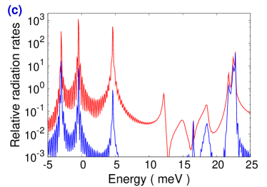
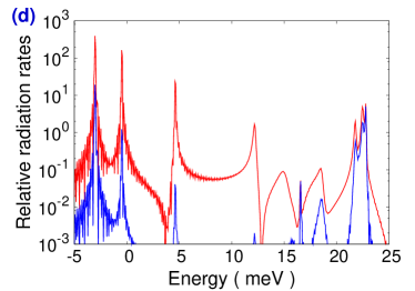
For FP cavities with 8 pairs of SiO2 and TiO2 layers (as in Fig. 5a) the cavity mode has a quality factor of , implying a cavity photon lifetime of 11 ps. However, excitons can decay radiatively into a broad range of very low quality leaky modes. This radiative decay is most rapid into leaky modes with energy lower than the cavity mode. The enhancement of radiation rate leads to sub-picosecond polariton lifetime. With 15 pairs of layers the FP cavity mode has a quality factor as high as implying a cavity photon lifetime of 1500 ps. As before, excitons can radiate through leaky modes (Figs. 5b and 5c) emerging from the sides of the FP. Radiation through leaky modes becomes weaker for the larger dipole size of than for the smaller dipole size of . Nevertheless, radiation lifetimes at the hot-spots are on the order of 1 ps. In the limit of an infinitely extended dipole contained in an FP cavity of infinite lateral extent, momentum conservation requires that all radiation is emitted into the cavity mode. However, in this case, BEC is excluded by the Mermin-Wagner theoremwagner .
Dielectric disorder in realistic SiO2-TiO2 FP’s reduces the polariton lifetime even below our calculated time scalestio2-fp . Moreover, at room temperature, excitons with energies away from strongly-coupled leaky modes but within the homogeneous linewidth (50 meVshen ) and phonon energy (43 meVLO-mose1 ) can be scattered efficiently (within ps) by phononsLO-mose2 to the leaky modes and then radiate rapidly. These effects reduce polariton lifetime to ps even for FP cavities with 15 pairs of layers and cavity quality factor of . The sub-picosecond lifetime of polaritons is still on the same order of magnitude with the phonon scattering time (about 0.1 ps) in MoSe2 at room temperatureLO-mose2 . In contrast, in a 3D PBG microcavity architecture with a microcavity embedded in a 3D PBG materialnoda ; noda6 , all leaky modes can be eliminated leading to very long polariton lifetime, limited only by exciton nonradiative decay. These nonradiative decay channels include Auger recombination arising from exciton-exciton collision and Shockley-Read-Hall recombination arising from electronic defects in the active semiconductor monolayers. Auger recombination is usually very inefficient in moderate to large band gap semiconductors such as MoSe2 for the moderate exciton densities we consider (volume density less than cm-3)zhao ; cdte . Recently high (electronic) quality, large area MoSe2 monolayers were successfully prepared by various methodscvd ; method2 ; method3 , exploiting the significant mechanical, chemical and thermal stability of MoSe2 monolayersmethod3 . In our architecture, the MoSe2 monolayers are encapsulated by TiO2 layers above and below, protecting them from defects introduced by wafer-fusion of the central slab to the photonic crystal. In well-fabricated samples, the polariton lifetime in our 3D PBG microcavities can be much longer than 130 ps, while efficient phonon scattering facilitates equilibration of the polariton gas in psLO-mose2 .
Effect of exciton inhomogeneous and homogeneous broadening
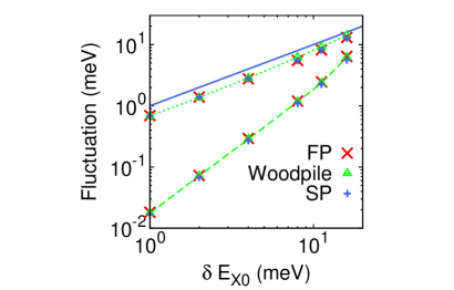
As a result of polariton motional narrowing, inhomogeneous broadening within a given monolayer has only a minor effect on BECyang1 ; yang2 ; book-kavo . Inhomogeneous broadening between different monolayers is modeled by a Gaussian random shift of the exciton emission energy in each monolayer, , . The root mean square deviation of the vacuum Rabi splitting and the polariton dispersion depth , calculated as a function of exciton inhomogeneous broadening , are shown in Fig. 6. The results for the three types of cavity are almost the same. The fluctuation of the vacuum Rabi splitting is considerably smaller than the exciton inhomogeneous broadening due to averaging among different monolayerscdte , whereas the fluctuation of the dispersion depth is comparable to . Nevertheless, for inhomogeneous broadening less than 10 meV, the dispersion depth remains larger than 48 meV enabling BEC up to 500 K (370 K) for the SP (woodpile) PC cavity.
Exciton homogeneous broadening is considerable in MoSe2 at room temperature due to phonon scatteringLO-mose2 . Optical measurements reveal a broadening of 50 meV in Ref. shen . Picosecond phonon scatteringLO-mose2 facilitates thermal equilibration of polaritons within several picoseconds. Homogeneous broadening slightly degrades the vacuum Rabi splitting and the polariton dispersion depth. If the homogeneous broadening is described by a imaginary part of exciton energy, , the vacuum Rabi splitting is reduced from meV to meV at zero detuning for meV. For a detuning of meV, exciton homogeneous broadening of meV reduces the lower-polariton dispersion depth by 5.5 meV. The highest transition temperature is then reduced from 590 K to 560 K. If an inhomogeneous broadening of 30 meV is taken into account as well, the transition temperature will be reduced to 430 K which is still above room-temperature. This suggests that polaritons in woodpile and SP PC microcavities are robust against electronic and photonic disorder and exciton homogeneous broadening, enabling above room-temperature polariton BEC in realistic systems.
References
- (1) Xiao D., Liu, G.-B., Feng, W., Xu, X. & Yao, W. Coupled spin and valley physics in monolayers of MoS2 and other group-VI dichalcogenides. Phys. Rev. Lett. 108, 196802 (2012).
- (2) Ross, J. S. et al. Electrical control of neutral and charged excitons in a monolayer semiconductor. Nat. Commun. 4, 1474 (2013).
- (3) Haug, H. & Koch, S. W. Quantum theory of the optical and electronic properties of semiconductors, Chap. 10, (World Scientific, 2009).
- (4) Ramasubramaniam, A. Large excitonic effects in monolayers of molybdenum and tungsten dichalcogenides. Phys. Rev. B 86, 115409 (2012).
- (5) Ugeda, M. M. et al. Observation of giant bandgap renormalization and excitonic effects in a monolayer transition metal dichalcogenide semiconductor. arXiv:1404.2331, Nat. Mater. in press.
- (6) Kumar, N., He, J., He, D., Wang, Y. & Zhao, H. Valley and spin dynamics in MoSe2 two-dimensional crystals. Nanoscale, 6, 12690 (2014).
- (7) Kumar, N. et al. Exciton-exciton annihilation in MoSe2 monolayers. Phys. Rev. B 89, 125427 (2014).
- (8) Mermin, N. D. & Wagner, H. Absence of ferromagnetism or antiferromagnetism in one- or two-dimensional isotropic Heisenberg models. Phys. Rev. Lett. 17, 1133-1136 (1966).
- (9) Bhattacharya, P. et al. Room temperature electrically injected polariton laser. Phys. Rev. Lett. 112, 236802 (2014).
- (10) Horzum, S. et al. Phonon softening and direct to indirect band gap crossover in strained single-layer MoSe2. Phys. Rev. B 87, 125415 (2013).
- (11) Jin, Z., Li, X., Mullen, J. T. & Kim, K. W. Intrinsic transport properties of electrons and holes in monolayer transition-metal dichalcogenides. Phys. Rev. B 90, 045422 (2014).
- (12) Ogawa, S., Imada, M., Yoshimoto, S., Okano, M. & Noda, S. Control of light emission by 3D photonic crystals. Science 305, 227-229 (2004)
- (13) Noda, S., Fujita, M., & Asano, T. Spontaneous-emission control by photonic crystals and nanocavities. Nature Photon. 1, 449-458 (2007).
- (14) Jiang, J. H. & John, S. Photonic crystal architecture for room temperature equilibrium Bose-Einstein condensation of exciton-polaritons. Phys. Rev. X 4, 031025 (2014).
- (15) Chamlagain, B. et al. ACS Nano 8, 5079-5088 (2014)
- (16) Wang, X. et al. Chemical vapor deposition growth of crystalline monolayer MoSe2. ACS Nano 8, 5125-5131 (2014).
- (17) Shim, G. W. et al. Large-area single-layer MoSe2 and its van der Waals heterostructures. ACS Nano 8, 6655-6662 (2014).
- (18) John, S. & Yang, S. Electromagnetically induced exciton mobility in a photonic band gap. Phys. Rev. Lett. 99, 046801 (2007).
- (19) Yang, S. & John, S. Exciton dressing and capture by a photonic band edge. Phys. Rev. B 75, 235332 (2007).
- (20) Kavokin, A. V. & Malpuech, G. Cavity polaritons (Elsevier, Amsterdam, 2003), chap. 3.