Contacts for organic switches with carbon-nanotube leads.
Abstract
We focus on two classes of organic switches operating due to photo- or field-induced proton transfer (PT) process. By means of the first-principles simulations, we search for the atomic contacts which strengthen diversity of the two swapped I-V characteristics between two tautomers. We emphasize, that the low-resistive contacts not necessarily possess good switching properties. Very often, the higher-current flow makes it more difficult to distinguish between the logic states. Instead, the more resistive contacts multiply a current gear to a larger extent. The low- and high-bias work regimes set additional conditions, which are fulfilled by different contacts: (i) in the very low-voltage regime, the direct connections to the nanotubes perform better than the popular sulfur contacts, (ii) in the higher-voltage regime, the best are the peroxide (-O-O-) contacts. Additionally, we find that the switching-bias value is not an inherent property of the conducting molecule, but it strongly depends on the chosen contacts.
pacs:
73.23.Ad, 73.63.Rt, 73.63.Fg, 71.15.MbI Introduction
Miniaturization caused mainly by the energy savings, speed and multi-functionality reasons is a strong driving force for the molecular basic research. The diodes, transistors, switches, memory cells, and sensors are currently designed from the molecular systems connected to the metallic or carbon leads.b1 Fabrication of organic devices is technologically simpler and its costs are lower. Thus, the search for organic substitutes of inorganic systems is a vigorous branch.b2 It is also dictated by the ecologic requirements since in the organic systems, the light atoms replace heavy - and toxic for the environment - elements. Moreover, the relatively new field of molecular electronics intensively stimulates the development of methods.b3
The metallic leads are widely used for nano-device electronics,b4 however recently, the carbon systems become more popular.b5 This is mainly due to the better thermoelectric efficiency - which is a separate subject of investigations including the vibronic effects.b6 ; b7 ; b8 ; b9 Therefore, we decided to use the carbon-nanotube (CNT) leads. To date, the carbon-system contacts to the metal leads were explored for C60,b10 ; b11 CNTb12 ; b13 and graphene.b13 ; b14
Various types of electrodes and nano-devices, as well as their functionalities, set requirements for the electronic contacts.b15 ; b16 Their role has been addressed a decade ago,b17 ; b18 and it is still of major importance.b19 ; b3 All types of devices seek the low-resistivity contacts in order to avoid large heat dissipation.b20 ; b21 ; b22 Additionally, some contacts are designed to be spin-selective.b23 Switches, however, need contacts which are low-resistive, and additionally they amplify the current gear obtained at the transition between two, or more, molecular forms; so an effect of the switched logic state is easily measured in the circuit. Finding such contacts is the main goal of our study, since – according to our knowledge – it was not addressed up to date.
Molecular switches work under various external triggering stimuli: electric or magnetic field, light, temperature, chemical reaction, mechanical stress, radiation, etc.b24 Here, we focus on two classes of the molecular switches, which operate under the photo- or field-stimuli. The first group can operate at very low voltage, since the tautomeric transition is triggered by light, not by bias. The second group works in the wide range of voltages, set by the values of swapping biases – which are different for the state-on and the state-off. These voltages typically are higher than the low-bias regime in which the photo-switches operate. The higher-bias regime is more demanding for the electronic contacts. Hence, it is much more difficult to obtain a high current gear for the field-switches than for the photo-switches.
In this work, we used the first-principles methods for the electronic-structure and ballistic-conductance calculations to obtain the current-voltage (I-V) curves for the tautomeric switches connected to the CNT leads. The studied photo- and field-switches base on the proton transfer between the oxygen and the nitrogen centers.b25 ; b26 ; b27 ; b28 ; b29 ; b30 The contacts are chosen among the light atoms or chemical groups: -C-, -CC-, -O-, -O-O-, -S-, -CS2-, -CH2-, -NH-, as well as the direct connection to the CNT. Some choices might appear fancy at the first sight, however the results on a nanoscale are often surprising.b31
Interestingly, the switching voltages are not the properties of the conducting molecules only, but they depend strongly on the selected contacts. Among the investigated in this work structures, the cases with multiple negative differential resistance (NDR) show up, and they were described in our previous work as candidates for the high-frequency devices.b32
II Results and discussion
It is a common practice that the sulfur contacts are used to connect a molecule to the metallic or carbon-based leads. Some authors connect the molecule directly to the graphene surface or the carbon nanotube.b33 Here, we check some other possibilities. Among others, we explore the properties of acetylene (-CC-), oxygen (-O-) and peroxide (-O-O-) contacts. Generally, the oxygen element is not popular as a contact. But when oxygen is added to some conductive structures, it can bring along a new physics.b34 ; b35 ; b36 Below, we report the results for the two types of molecular switches: triggered either by light or by voltage; both are based on the proton transfer (PT) reaction along the intramolecular hydrogen-bond.
II.1 Photo-switches: low-voltage work regime
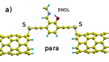
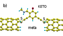
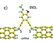
The photo-switches discussed in this subsection, differ from the discussed hereafter field-switches by the fact, that their two photo-tautomeric structures form due to reversible photoinduced intramolecular proton-transfer process - while the field-switching induces this reaction in the ground electronic state. Photo-switching of molecular conductance is studied for the two stable isomers of salicylidene methylamine (SMA).b27 ; b28 The photo-induced PT reaction occurs between the oxygen atom of the hydroxyl group and the nitrogen atom of the amino group of SMA.b30 Both respective photo-tautomeric forms - called the enol and keto - are presented in Fig. 1. Additionally, these forms differ from each other by the conformation of the methylamine tail with respect to the salicylidene core.b27 Importance of the contact geometry for the transport properties has been shown for many systems.b10 ; b37 ; b38 ; b39 ; b40 Moreover, the properties of the junction may also depend on the CNT chirality, thus, all carbon electrodes considered in this work are of the zigzag type - the most effective form for the switches.b41
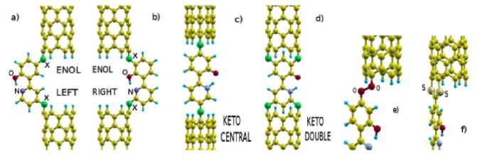
Following the work by Staykov et al.,b30 we simulate transport in various structural connections to the leads: para, meta, and not studied earlier ortho - all displayed in Fig. 1. But our main aim is to check the switching impact of contacts, such as the direct connection, O and S atomic connections. The S and O connections form the angular structures with the CNT (about 105-120 deg). In contrast, the direct connection is linear. Additionally, the electronic conjugation of the phenyl ring of SMA is extended by acetylenic moieties attached on its both sides; so-called anchor groups. Former studies of these molecules framed, however, between the metallic electrodes, have revealed that the meta connection is much more efficient for the photo-switching than the para one.b30 In this work, we considered also the ortho structure. The obtained I-V curves are presented in Fig. 2 (details of the calculations are given in the methods section).
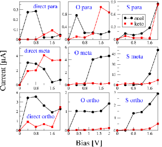
Focusing on the resistivity of the contacts and the connecting structures, generally it is not surprising that the sulfur atom is the best conductive contact within the range of applied bias (about 2V). The meta structures are much more conductive than the para, and also more than the ortho. With an exception that for the direct connection, the meta and ortho geometries show similar currents for the enol and keto structures below 2V. Transition voltages, in a sense of the voltage at which the current rises from zero for very small applied biases,b42 are usually lower for -O- than -S-, and are the lowest for the direct connection. This fact sets the working bias-regimes: Vwork(direct) Vwork(O) Vwork(S).
Further inspection of the results presented in Fig. 2 leads to the following conclusions: (i) the most interesting result with respect to the current gain between the two isomeric forms at very low bias, up to 0.4V, is obtained for the cases: direct- and oxygen para and ortho, but it is not the case with the S contact, (ii) for the voltage around 2V, the best performing switches are: oxygen contacts and direct-meta, and S-meta and -ortho. For some cases, the negative differential resistance is observed - especially with the direct contacts. This effect, however, does not exclude the device from operation if we choose the proper working bias-range (0.4-0.8V).
II.2 Field-switches: higher-voltage work regime
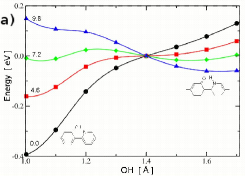
The electric field applied to the molecule may tune the shape of the energetical landscape of the ground-electronic state and thus, it may change the relative stability of the two tautomeric forms of the molecule. One form which is the most stable without the E-field may become less stable or even unstable in the higher voltage values which favor another tautomeric form. In the studied case the enol form is the only stable form when no filed is applied, (see Fig 3a, black filled circles). To stabilize the keto form one must apply the electric field along the main exes of the molecule, which is also the direction of the proton transfer between the oxygen and nitrogen atoms which transforms enol into the keto form. Thus, the distance between the oxygen and hydrogen atoms, R(OH), is the best choice of a driving coordinate for an illustrative description of the process. To characterize the process in more detail, we construct the minimum-energy profile (MEP) along the driving coordinate. Along the MEP, all the intramolecular nuclear degrees of freedom are optimized for a given frozen value of the driving coordinate R(OH). Separate ground-state MEPs are calculated for different values of the electric field applied to the molecule. Bias values in V are given in Fig. 3a above the corresponding MEP additionally distinguished with shape and color Those indicate changes in the ground-state energy landscape: the heights of the enol-to-keto and keto-to-enol tautomerization-reaction barriers and the stabilization energy of both forms. MEPs plotted in Fig. 3a represent relative energy normalized at R(OH)=1.4 Å.
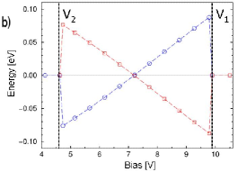
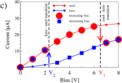
Potential-energy profiles sketched in Fig. 3a result in a ’hysteresis’ of the field-induced switching between the tautomeric forms of the 2PPy molecule terminated with the methyl groups. The ‘hysteresis’ curve presented in Fig. 3b represents minimum-energy of a given tautomeric form normalized vs. the mean energy of both tautomeric forms (the zero-energy of the scale) at the applied value of bias. One can see that both tautomeric forms of 2PPy can coexist within a given range of the applied voltage, the terminal values of which define the limits V1 and V2, where the PT process enol-to-keto and keto-to-enol takes place, respectively. The switching values of the voltage impose the limits on the I-V characteristics computed for a given tautomeric form (Fig. 3c). The operation mode of the device is as follows: we start from the enol form, and when the voltage is increased to the value higher than V1, the molecule switches to the keto form. Then, the bias is decreased down to the second switching voltage V2, and the reversed transformation to the enol form occurs. This effect shows up as a jump of the current flowing via the molecule (Fig. 3c).
Similarly to the photo-switches discussed above, also for the field-switches, different geometric connections to the CNT can be realized; they are presented in Fig. 4a-4d. In Fig. 4e, we show the zigzag geometry of the peroxy (-O-O-) contact, in contrast to the linear geometry of the acetylenic (-CC-) one. The contact via the CS2 planar group is depicted in Fig. 4f. It is interesting to explore the CS2 group, since it has been announced as very low-resistive contact for gold leads, characterized by low electronic work-function.b20 ; b43 To complete these studies, we add also the -NS2- connection to our list (in the same geometry as the -CS2- contact). It has been experimentally evidenced that the field-switching is a robust property of a molecule, and not a stochastic phenomenon.b44 We show in this work, that the switching effect is not only a property of the molecule but also strongly depends on the chosen contact. As one may notice inspecting Fig. 4, the single-branched contacts might be arranged to the 2PPy switch in the three-fold manner as: ’left’, ’right’- or ’central’ configuration. The double-branched contacts were studied earlier by us and showed the negative differential resistance,b32 which in some cases can exclude the system as a candidate for a switch.
| V1 | V2 | V1 | V2 | |
| contacts | E-K | K-E | E-K | K-E |
| double-branch | single-branch central | |||
| bare molecule(1) | 6.2 | 2.6 | ||
| -CH2- | 6.6 | 2.0 | 9.7 | 4.3 |
| -NH- | 5.4 | 1.4 | 10.3 | 5.4 |
| -O- | 7.2 | 2.9 | 10.1 | 5.3 |
| -S- | 6.2 | 2.1 | 8.7 | 4.9 |
| direct(2) | 8.9 | 3.1 | ||
| -CC- | 15.9 | 5.6 | ||
| -O-O- | 11.5 | 5.7 | ||
| -CS2-(3) | 15 | 15 | ||
| -NS2-(3) | 15 | 15 | ||
| single-branch left | single-branch right | |||
| -CH2- | 8.6 | 3.7 | 7.1 | 2.0 |
| -NH- | 7.9 | 4.2 | 6.3 | 1.4 |
| -O- | 7.7 | 4.1 | 7.7 | 2.4 |
| -S- | 8.0 | 3.4 | 7.5 | 2.1 |
| (1) molecule is ’free-standing’, not connected to leads | ||||
| (2) molecule is directly connected to leads | ||||
| (3) the enol to keto transition was not found up to 15V | ||||
In Table 1, we collect the high, V1, and the low, V2, transition voltages determined for various contacts and structures presented in Fig. 4a-4d. For completeness, we also show the tautomeric switching biases for the bare molecule - not connected to the leads. Inspection of these results leads to the following conclusions: (i) the operating voltage range for a given tautomeric form, V1-V2, is relatively wide (several volts), (ii) various contacts and structures introduce large diversification of the work regimes. What is very important, the relatively large switching bias in some cases is perhaps too high for technological applications. It is generally more practical, for stability reasons, to utilize the device operating under a lower transition (V2). Although, in reality the theoretically predicted demands are overestimated. The calculated bariers would be much smaller when the temperature, vibrational, interface and tunneling effects were included.AJ Analyzing the results obtained for different connections presented in Table 1, one may state that the double-branch and ’right’-single-branch structures seem to be the best promising choice (smaller V2). While the larger V2 values are given for the ’left’-single-branch connections, and the single-branch ’central’ connections are characterized by the highest switching biases. On the other hand, as we will see hereafter, the latter case is the only non-NDR case which is stable with respect to switching.
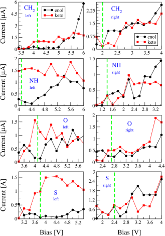
The I-V curves computed for single-branch side connections, ’left’ and ’right’, are depicted in Fig. 5. These curves correspond to the structures shown in Fig. 4a-4d. The NDR effect seen in some cases is very often detected in the triangular lattices, such as graphene and some organic molecules.b45 Here, we observe the NDR for the single-branch ’left’- and ’right’-side structures (Fig. 5), and this effect is even stronger than for the double-branch case.b32 This is generally an undesired effect with respect to the switching performance. Some remedy for this problem possibly could be found using longer anchor groups, since a suppression of the quantum conductance oscillations (leading also to the NDR effect) was reported.b46 On the other hand, the energetic barriers to be conquered in the course of the PT process are not very high (c.f. Fig. 3a) and the vibrational or thermal effects may lower them, as mentioned earlier. Thus, moving the transitions to the next bias-point (V1 to lower, and V2 to higher) narrowing the hysteretic loop and shifting the operation region to the non-NDR part. The work regimes, chosen for the lower transitions at V2, are marked in the I-V characteristics by dashed green lines. Despite the NDR effect existing in all cases in Fig. 5, the -NH- and -S- ’left’-side contacts seem to be promissing for technological applications, due to a large gear of the enol and keto currents in the vicinity of the switching bias.
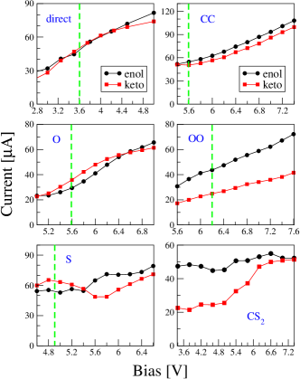
Finally, the single-branch central structures were analyzed with respect to their I-V properties; the results are presented in Fig. 6. One can notice, upon inspection of the figure, that the keto to enol switching voltage is the lowest for the case of the direct connection to the leads. Moreover, for the direct contact, as well as for the acetylenic (-CC-) and oxygenic (-O-) bridges, the I-V curves of two tautomers are almost identical to each other. It is not surprising result, since for the high voltage the following observations are true:
-
•
the range of the quantum-conductance function entering the current equation (see methods section) is large,
-
•
the projected density of states (PDOS) of the O-H-N group in the enol and keto structures lay closer to the Fermi level than the voltage range which enters the I-V formula.
Therefore, all details differentiating one tautomer from the other are summed-up in the transmission function to the similar values of the current. If the operating voltage range falls within the range where the characteristic parameters of the tautomers differ, then the current curves of the tautomers also differ.
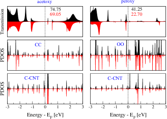
The most important result of this section is the conclusion that for the peroxy (-O-O-) contact, a good current-gear for the switching at high voltage (5V) is obtained. It is not advantageous property of the peroxy contacts that they are more resistive than the acetylenic ones (-CC-). But the peroxy contacts strengthen the diversity of the conductances of different molecular structures - and this is what we need.
Since the sulfur contact is an electron-rich and highly polarizable moiety, the existence of undesired NDR effect in this case is not surprising for larger biases.b45 We obtained nicely separated enol and keto current curves for -CS2- at voltages between 3.5V and 5.5V. It is of little practical use, however, due to the fact that the switching voltage with increasing bias (V1) is for this contact higher than 15V - up to the checked PES (see Table 1); and we did not observe switching to the keto structure. Also the current values for the enol and keto forms show a tendency to join each other at biases higher than 6V.
II.3 Transmission and the projected density of states
The electrical conductivity can be derived from the orbitals hybridization of the conducting molecule, atomic contacts and the leads - those orbitals, which energetically lay close to the Fermi level. Therefore, plots of the PDOS tell us about reasons for the existence of the quantum conductance peaks or their absence. Of course, not all states visible on the PDOS plots contribute to the current. In our systems, there are the lone electron pairs and the molecular orbitals orthogonal to the conduction direction. On the other hand, it is trivial that the lack of states in some energetic region results to no current.
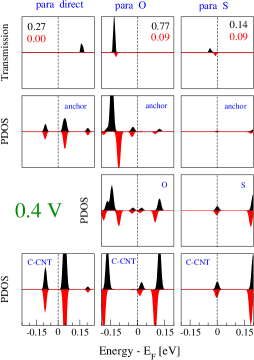
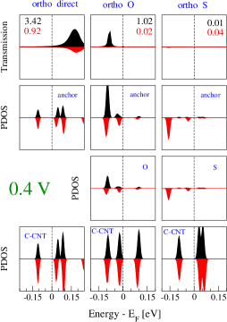
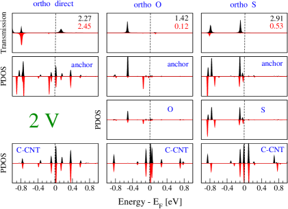
In Figs. 7 and 8, we plot the quantum conductance (QC) and PDOS of photo- and field-switches for selected contacts, for which the I-V curves were presented in Figs. 2 and 6. The electric fields at which the QC and PDOS plots have been obtained correspond to the bias 0.4V and 2V for the photo-switches (in Fig. 7) and 6V for the field-switches (in Fig. 8). For convenience, the corresponding values of the current [in A] are written in the top panels.
Transition voltage is the bias at which the current starts to grow from zero.b42 In the case of photo-switches operating at very low bias regime, the working voltages of the device are in the range where the enol and keto forms show different transition voltages. The lowest transition biases are for the direct contact, medium for oxygen and higher for the sulfur contacts. Following the discussion by Wu et al.,b42 the largest transition voltages are obtained for those atomic contacts whose -states lay higher in the energy above the Fermi level. This is also true for the photo-switches and the PDOS presented in Fig. 7. The position of the -states of the anchor group and the contact and the terminal carbon of the CNT lead is the highest in a case of the sulfur contact. For the direct contacts, these states are the most close to the Fermi level of all studied connections. The above sequence corresponds to the obtained current gears. The states which originate from the lonely pairs, or the orbitals non-overlapping with the conduction axis, do not contribute to the quantum conductance.
As for the resistance related problems, it has been stressed in many reports - for instance in the recent work by Schulz et al.b20 - that the Fermi level mismatch of the conductor and leads is responsible for the low conductance. Actually, for a good the switch, one tautomeric form should be very resistive and the other well conducting in the device-operating bias region. In contrast to the bias regime of 0.4V (upper panels), for 2V (lower panel) the best performing contact is that with sulfur, and the next of oxygen. The low transition bias of the direct contacts does not work for the switch in the higher voltage range. This is because all PDOS diversities of the enol and keto forms are summed-up to similar values when the bias range is larger. Instead, for the oxygen and sulfur contacts, not all PDOS mismatches between two tautomers appear in the bias range of 2V.
For the field-swithes operating at higher voltages - around 5-6V - the situation is more difficult. One needs to find such contacts, that the nonsymmetric contributions to the PDOS from the tautomers do not sum-up in the QC to similar values of current. In a case of the -CC- contacts, the quantum conductance spectra of tautomers are nonsymmetric but sum to the similar currents (see Fig. 8). On the other hand, the nonsymmetric QC spectra of the peroxy contacts give a good current gear. After inspection of the PDOS in the range of [-3,3] eV, the intensities of the acetoxy states are much smaller than the states of the peroxy case. Therefore, the tautomeric diversity is strengthened in the peroxy-contacts case, and they are the only contacts - of all studied here - which could work for the field-switches.
Since the energetic positions of the contact states are very important, we emphasize that the simple DFT method does not reproduce them well. One should go beyond this approximation, and for instance the self-interaction corrections (ASIC) and the constrained DFT (CDFT) method have been applied for the effect of the hydrogenetation on the sulfur contacts in the BDT-gold molecular junction.b47 On the other hand, our leads and conductors are mainly carbonic, and not metallic. In contrast to the large underestimation of the energy gap in diamond by simple DFT scheme, the carbonic conductive systems, such as graphene and carbon nanotubes, are well described within this method - the same as the band structures of simple metals. The DFT failur very strongly shows up when the metallic and non-metallic elements are combined, and the localized atomic-like -states (or -states) form. The relative position of these metallic states, with respect to the -states of the non-metallic atoms, is usually placed too shallow below the Fermi level (or the highest occupied molecular orbital, HOMO, level). Similarly, the corresponding energies of the unoccupied metallic-states reside too low above the conduction band minimum (or the lowest unoccupied molecular orbital, LUMO, level). Such situation leads to large overestimation of the calculated conductance. The systems studied in this work are purely non-metallic, therefore, they are free of the above described mismatch of the two kinds of the energy levels.
Since in this work, we studied an impact of the geometry on the current, another interesting phenomenon could be addressed in a future work - namely, the current-driven geometric and electronic structure rearrangements. These effects would lead to the non-linear conduction characteristics and different switching properties. Such studies within the time-dependent Ehrenfest formalism were reported for the metallic clusters.b48
III Conclusions
We searched for electronic contacts which strengthen the switching properties of the molecular devices based on the intramolecular proton transfer process. Two classes of model molecular photo- and field-switches, operating at lower- and higher-bias work regime, respectively, were analyzed. By means of the first-principles electronic calculations, we found the electronic structure, Wannier functions, and the electronic transport properties (the I-V curves).
The larger difference between the currents of the swapped structures, the better is the performance of a switch. Moreover, we would like to have low-resistive contacts, but the mechanism of the current on-off switching with applied bias and the rules governing the resistance stay in the opposition to each other. It is demonstrated that for very low- and higher-bias work regimes, the efficient contacts are chosen according to different effects: (i) the transition voltage for the current-on switch and (ii) the resistive conformational selectivity, respectively. The low-bias operating range (0.5V) of photo-switches prefers the direct connection with leads, which is low-resistive. For the middle voltage work regime (1-2V), the oxygen or sulfur are the best atomic contacts. The high-bias operating range (4V) of the field-switches choses the peroxy contacts.
In addition, we found that the transition voltages of the field-switches
are very sensitive to the choice of contacts. This is caused mainly
by differences in the polarizabilities of the atomic contacts.
IV Methods
We performed the density-functional theoryb49 calculations of the molecules between the CNT leads using the plane-wave Quantum ESPRESSO code.b50 These self-consistent runs were repeated for many discrete external electric fields with a step visible in the reported figures. Then the obtained Bloch functions were used to generate maximally localized Wannier functions (MLWF)b51 ; b52 employing the wannier90-2.0.0 code.b53 The same package was then utilized for the transport calculations within the Landauer-Büttiker scheme.b54 The obtained quantum conductance (or transmission) for each electric field, T(;EV), was embedded in the equationb55
with the Fermi-Dirac distribution f(). This way, we reach the current I at the bias V which is equivalent to the external electric field E assumed in the DFT calculations.
To estimate the voltage values necessary to switch the transistor forms, the enol to the keto and back to the enol, we optimized the geometry of the molecule at discrete values of the applied electric field (with the step of 0.001 a.u.). The DFT method implemented in TURBOMOLE [57] was used in these calculations along with the B3LYP functional and correlation-consistent valence double-zeta atomic basis set with polarization functions for all atoms (cc-pVDZ)b57 for thoroughly studied exemplar PPy molecule terminated with methyl groups. For all other PPy derivatives the default def-SV(P) basis set was used in search of their characteristic V1 and V2 switching bias values.
As for the plane-wave calculations setup, the BLYP functional was used.
The energy cutoff for the plane-waves in the
Quantum Espresso code was set to 30 Ry, and the pseudopotentials were of
the Martin-Trouliers type from the Fritz-Haber Institute library.
In the quantum conductance calculations, each lead was built by the two CNT
units, and the conductor region included the molecule with the contacts and one
CNT ring saturated with hydrogens on the left- and right- lead side.
The figures representing the molecular geometry have been
prepared with the XCrySDen package.b58
Acknowledgements
This work has been supported by the research projects of the National Science Centre of Poland, Grant No. 2012/04/A/ST2/00100. Calculations were done in the Interdisciplinary Centre of Mathematical and Computer Modeling (ICM) of the University of Warsaw within the grants G47-7, G56-32 and G29-11.
References
- (1) Aradhya, S. V.; Venkataraman, L. Single-molecule junctions beyond electronic transport. Nature Nanotechnology 8, 399–12.
- (2) Facchetti, A. Organic semiconductors: Made to order. Nature Materials 12, 598–3.
- (3) Ortmann, F.; Radke, K. S.; Günther, A.; Kasemann, D.; Leo, K.; Cuniberti, G. Materials Meets Concepts in Molecule-based Electronics. accepeted to Adv. Func. Mat., DOI:10.1002/adfm.201402334.
- (4) Perrin, M. L.; Verzijl, C. J. O.; Martin, C. A.; Shaikh, A. J.; Eelkema, R.; van Esch, J. H.; van Ruitenbeek, J. M.; Thijssen, J. M.; van der Zant, H. S. J.; Dulic, D. Large tunable image-charge effects in single-molecule junctions. Nature Nanotechnology 8, 282-6.
- (5) Avouris, P.; Chen, Z.; Perebeinos, V. Carbon-based electronics. Nature Nanotechnology 2, 605-11.
- (6) Benesch, C.; C̆íz̆ek, M.; Klimes̆, J.; Kondov, I.; Thoss, M.; Domcke, W. Vibronic Effects in Single Molecule Conductance: First-Principles Description and Application to Benzenealkanethiolates between Gold Electrodes. J. Phys. Chem. C 112, 9880–11.
- (7) Huang, Z.; Chen, F.; D’agosta, R.; Bennett, P. A.; Di Ventra, M.; Tao, N. Local ionic and electron heating in single-molecule junctions. Nature Nanotechnology 2, 698-6.
- (8) Kim, S.; Marzari, N. First-principles quantum transport with electron-vibration interactions: A maximally localized Wannier functions approach. Phys. Rev. B 87, 245407-11.
- (9) Tsutsui, M.; Kawai, T.; Taniguchi, M. Unsymmetrical hot electron heating in quasi-ballistic nanocontacts. Sci. Rep. 2, 217-7.
- (10) Frederiksen, T.; Foti, G.; Scheurer, F.; Speisser, V.; Schull, G. Chemical control of electrical contact to sp2 carbon atoms. Nature Commun. 5, 3659-7.
- (11) Schull, G.; Frederiksen, T.; Arnau, A.; Sanchez-Portal D.; Berndt, R. Atomic-scale engineering of electrodes for single-molecule contacts. Nature Nanotechnology 6, 23-5.
- (12) Nemec, N.; Tomanek, D.; Cuniberti, G. Contact dependence of carrier injection in carbon nanotubes: An Ab Initio study. Phys. Rev. Lett. 96, 076802.
- (13) Leonard, F.; Talin, A. A. Electrical contacts to one- and two-dimensional nanomaterials. Nature Nanotechnology 6, 773-11.
- (14) Xia, F.; Perebeinos, V.; Lin, Y.-M.; Wu, Y.; Avouris, P. The origins and limits of metal–graphene junction resistance. Nature Nanotechnology 6, 179-6.
- (15) Nitzan, A.; Ratner, M. A. Electron Transport in Molecular Wire Junctions. Science 300, 1384-6.
- (16) Agraït, N. A.; Yeyati, L.; van Ruitenbeek, J. M. Quantum properties of atomic-sized conductors, Phys. Rep. 377, 81-198.
- (17) Cuniberti, G.; Grossmann, F.; Gutierrez, R. The role of contacts in molecular electronics. Advances in Solid State Physics 42, 133–17.
- (18) Zhirnov, V. V.; Cavin, R. K. Molecular electronics: Chemistry of molecules or physics of contacts? Nature Mater. 5, 11–2.
- (19) Weiss, D. The importance of contacts. Nature Phys. 5, 859.
- (20) Schulz, P.; Sch afer, T.; Zangmeister, C. D.; Effertz, C.; Meyer, D.; Mokros, D.; van Zee, R. D.; Mazzarello, R.; Wuttig, M. A New Route to Low Resistance Contacts for Performance-Enhanced Organic Electronic Devices. Adv. Mater. Interfaces 1, 1300130-8.
- (21) Moon, J. S.; Antcliffe, M.; Seo, H. C.; Curtis, D.; Lin, S.; Schmitz, A.; Milosavljevic, I.; Kiselev, A. A.; Ross, R. S.; Gaskill, D. K.; Campbell, P. M.; Fitch, R. C.; Lee, K.-M.; Asbeck, P. Ultra-low resistance ohmic contacts in graphene field effect transistors. Applied Physics Letters 100, 203512.
- (22) Chai, Y.; Hazeghi, A.; Takei, K.; Chen, H.-Y.; Chan, P. C. H.; Javey, A.; Wong, H.-S. P. Low-Resistance Electrical Contact to Carbon Nanotubes With Graphitic Interfacial Layer. IEEE Trans Electr. Dev. 59, 12-8.
- (23) Guo, A.-M.; Gaul, E. D, C.; Gutierrez, R.; Dominguez-Adame F.; Cuniberti, G.; Sun, Q.-F.; Contact effects in spin transport along double-helical molecules. Phys. Rev. B 89, 205434.
- (24) Fuentes, N.; Martín-Lasanta, A.; de Cienfuegos, L. A.; Ribagorda, M.; Parra, A.; Cuerva, J. M. Organic-based molecular switches for molecular electronics. Nanoscale, 3, 4003-12.
- (25) Hofmeister C.; Härtle, R.; Rubio-Pons, Ó.; Coto, Pedro B.; Sobolewski, A. L.; Thoss, M. Switching the conductance of a molecular junction using a proton transfer reaction. J. Mol. Model. 20, 2163.
- (26) Benesch, C.; Rode, M. F.; c̆íz̆ek, M.; Härtle, R.; Rubio-Pons, O.; Thoss, M.; Sobolewski, A. L. Switching the Conductance of a Single Molecule by Photoinduced Hydrogen Transfer. J. Phys. Chem. C 113, 10315-4.
- (27) Jankowska, J.; Rode, M. F.; Sadlej, J.; Sobolewski, A. L. Photophysics of Schiff Bases: Theoretical Study of Salicylidene Methylamine. ChemPhysChem 13, 4287-8.
- (28) Jankowska, J.; Rode, M. F.; Sadlej, J.; Sobolewski, A. L. Excited-State Intramolecular Proton Transfer: Photoswitching in Salicylidene Methylamine Derivatives. ChemPhysChem 15, 1643-10.
- (29) Grzegorzek, J.; Filarowski, A.; Mielke, Z. The Photoinduced Isomerization and its Implication in the Photo-dynamical Processes in Two Simple Schiff Bases Isolated in Solid Argon. Phys. Chem. Chem. Phys. 13, 16596-9.
- (30) Staykov, A. T.; Watanabe, M.; Ishihara, T.; Yoshizawa, K. Photoswitching of Conductance through Salicylidene Methylamine. Just accepted in J. Phys. Chem. C, DOI: 10.1021/jp5081884.
- (31) Simbeck, A. J.; Lanzillo, N.; Kharche, N.; Verstraete, M. J.; Nayak, S. K. Aluminum Conducts Better than Copper at the Atomic Scale: A First-Principles Study of Metallic Atomic Wires. ACS Nano 6, 10449–7.
- (32) Sadek, M.; Wierzbowska, M.; Rode, M. F.; Sobolewski, A. L. Multipeak negative differential resistance from interplay between nonlinear Stark effect and double-branch current flow. RSC Adv. 4, 52933-7.
- (33) Qian, H.; Lu, J.-Q. Molecular electronic switch using Carbon nanotube electrodes. Physics Letters A 371, 465–4.
- (34) Rocha, A. R.; Archer, T.; Sanvito, S. Is magnetoresistance in excess of 1,000 Phys. Rev. B 76, 054435.
- (35) Wohlthat, S.; Pauly, F.; Viljas, J. K.; Cuevas, J. C.; Schön, G. Ab initio study of charge transport through single oxygen molecules in atomic aluminum contacts. Phys. Rev. B 76, 075413.
- (36) Aradhya, S. V.; Frei, M.; Halbritter, A.; Venkataraman, L. Correlating Structure, Conductance, and Mechanics of Silver Atomic-Scale Contacts. ACS Nano 7, 3706–7.
- (37) Quek, S. Y.; Kamenetska, M.; Steigerwald, M. L.; Choi, H. J.; Louie, S. G.; Hybertsen, M. S.; Neaton, J. B.; Venkataraman, L. Mechanically controlled binary conductance switching of a single-molecule junction. Nature Nanotech. 4, 230–5.
- (38) Perrin, M. L.; Prins, F.; Martin, C. A.; Shaikh, A. J.; Eelkema, R.; van Esch, J. H.; Briza, T.; Kaplanek, R.; Kral, V.; van Ruitenbeek, J. M.; van der Zant, H. S. J.; Dulic, D. Influence of the Chemical Structure on the Stability and Conductance of Porphyrin Single-Molecule Junctions. Angew. Chem. Int. Ed. 50, 11223-4.
- (39) Diez-Perez, I.; Hihath, J.; Hines, T.; Wang, Z.-S.; Zhou, G.; Müllen, K.; Tao, N.; Controlling single-molecule conductance through lateral coupling of π orbitals. Nature Nanotech. 6, 226-6.
- (40) Wu, S.; González, M. T.; Huber, R.; Grunder, S.; Mayor, M.; Schönenberger, C.; Calame, M. Molecular junctions based on aromatic coupling. Nature Nanotech. 3, 569–6.
- (41) del Valle, M.; Gutierrez, Rafael; Tejedor, C.; Cuniberti, G. Tuning the conductance of a molecular switch. Nature Nanotech. 2, 176–4.
- (42) Wu, K.; Bai, M.; Sanvito, S.; Hou, S. Transition voltages of vacuum-spaced and molecular junctions with Ag and Pt electrodes. J. Chem. Phys. 141, 014707.
- (43) Li, Z.; Smeu, M.; Park, T.-H.; Rawson, J.; Xing, Y.; Therien, M. J.; Ratner, M. A.; Borguet, E. Hapticity-Dependent Charge Transport through Carbodithioate-Terminated [5,15-Bis(phenylethynyl)porphinato]zinc(II) Complexes in Metal−Molecule−Metal Junctions. Nano Letters 14, 5493-7.
- (44) Blum, A. S.; Kushmerick, J. G.; Long, D. P.; Patterson, C. H.; Yang, J. C.; Henderson, J. C.; Yao, Y.; Tour, J. M.; Shashidhar, R.; Ratna, B. R. Molecularly inherent voltage-controlled conductance switching. Nature, 4, 167-6.
- (45) Alemani, M.; Peters, M. V.; Hecht, S.; Rieder, K.-H.; Moresco, F.; Grill, L. J. Am. Chem. Soc. 128, 14446.
- (46) Bułka, B. R.; Kostyrko, T.; Łuczak, J.; Linear and nonlinear Stark effect in a triangular molecule. Phys. Rev. B 83, 035301.
- (47) Péterfalvi, C. G; Lambert, C. J. Suppression of single-molecule conductance fluctuations using extended anchor groups on graphene and carbon-nanotube electrodes. Phys. Rev. B 86, 085443.
- (48) de Melo Souza, A.; Rungger, I.;Pontes, R. B.; Rocha, A. R.; da Silva, A. J. R.; Schwingenschloegl, U.; Sanvito, S. Stretching of BDT-gold molecular junctions: thiol or thiolate termina-tion? Nanoscale 6, 14495-13.
- (49) Todorović, M.; Bowler, D. R. Non-adiabatic simulations of current-related structural transformations in metallic nanodevices. J. Phys. Condens. Matter 23, 345301.
- (50) Kohn W.; Sham, L. J. Self-Consistent Equations Including Exchange and Correlation Effects. Phys. Rev. 140, A1133.
- (51) Giannozzi, P.; Baroni, S.; Bonini, N.; Calandra, M.; Car, R.; Cavvazzoni, C. QUANTUM ESPRESSO: a modular and open-source software project for quantum simulations of materials. J. Phys. Condens. Matter 21, 395502-19; available from http://www.quantum-espresso.org.
- (52) N. Marzari, D. Vanderbilt, Maximally localized generalized Wannier functions for composite energy bands, Phys. Rev. B 56, 12847-19.
- (53) Marzari, N.; Mostofi, A. A.; Yates, J. R.; Souza, I.; Vanderbilt, D. Maximally localized Wannier functions: Theory and applications. Rev. Mod. Phys. 84, 1419-57.
- (54) A. A. Mostofi, J. R. Yates, Y.-S. Lee, I. Souza, D. Vanderbilt and N. Marzari, wannier90: A tool for obtaining maximally-localised Wannier functions. Comp. Phys. Comm. 178, 685-15.; available from http://www.wannier.org.
- (55) Büttiker, M.; Imry, Y.; Landauer, R.; Pinhas, S. Generalized many-channel conductance formula with application to small rings. Phys. Rev. B 31, 6207-9.
- (56) Brandbyge, M.; Mozos, J.-L.; Ordejon, P.; Taylor, J.; Stokbro, K. Density-functional method of nonequilibrium electron transport. Phys. Rev. B 65, 165401.
- (57) TURBOMOLE V6.3 2011, a development of University of Karlsruhe and Forschungszentrum Karlsruhe GmbH, 1989-2007, TURBOMOLE GmbH, since 2007; available from http://www.turbomole.com .
- (58) Dunning, T. H., Jr. Gaussian Basis Sets for Use in Correlated Molecular Calculations. I. The Atoms Boron Through Neon and Hydrogen. J. Chem. Phys. 90, 1007.
- (59) Kokalj, A. Computer graphics and graphical user interfaces as tools in simulations of matter at the atomic scale Comp. Mater. Sci. 28, 155.