Atomistic analysis of the impact of alloy and well-width fluctuations on the electronic and optical properties of InGaN/GaN quantum wells
Abstract
We present an atomistic description of the electronic and optical properties of N/GaN quantum wells. Our analysis accounts for fluctuations of well width, local alloy composition, strain and built-in field fluctuations as well as Coulomb effects. We find a strong hole and much weaker electron wave function localization in InGaN random alloy quantum wells. The presented calculations show that while the electron states are mainly localized by well-width fluctuations, the holes states are already localized by random alloy fluctuations. These localization effects affect significantly the quantum well optical properties, leading to strong inhomogeneous broadening of the lowest interband transition energy. Our results are compared with experimental literature data.
pacs:
78.67.De, 73.22.Dj, 73.21.Fg, 77.65.Ly, 73.20.Fz, 71.35.-yOver the last twenty years, research into nitride-based semiconductor materials (InN, GaN, AlN and their respective alloys) has gathered pace. This stems from their potential to emit light over a wide spectral range, making them highly attractive for different applications. Humphreys (2008) Despite very high defect densities, blue emitting InGaN-based devices exhibit high quantum efficiencies. Nakamura (1998); Oliver et al. (2010) The widely accepted explanation for this is that the carriers are spatially localized due to alloy fluctuations and are thus prevented from diffusing to defects. Nakamura (1998); Chichibu et al. (2006); Schöming et al. (2004); Oliver et al. (2010) The impact of alloy fluctuations on the electronic and optical properties in -plane InGaN/GaN quantum wells (QWs) has been further evidenced experimentally, e.g., by the “S-shape” temperature dependence of the peak photoluminescence (PL) energy. Wang et al. (2012); Hammersley et al. (2012) It is important to note that in wurtzite (WZ) InGaN systems the effect of these fluctuations is much more severe compared to that found, e.g., in zinc-blende (ZB) InGaAs alloys. This originates from the very different physical properties (e.g., band gap and lattice spacing) of the binary constituents (InN and GaN). Humphreys (2008); Oliver et al. (2010) A further complication is that InGaN/GaN QWs, compared with InGaAs/GaAs wells, exhibit much stronger electrostatic built-in fields, arising in part from the strain dependent piezoelectric response. Bernardini et al. (1997) Thus, alloy fluctuations in InGaN/GaN QWs affect the electronic structure through a complicated interplay of local alloy, strain, and built-in field fluctuations.
Even though the importance of alloy fluctuations has been experimentally evidenced, they have been widely neglected in the modeling of WZ InGaN/GaN QWs. Previous atomistic calculations have mainly focused on ZB Lee and Wang (2006); Wu et al. (2009); Chan et al. (2010) or WZ Gorczyca et al. (2009); Liu et al. (2010); Moses et al. (2011); Pela et al. (2011) InGaN bulk alloys. Properties of WZ InGaN/GaN QWs with realistic dimensions are typically studied using continuum-based theoretical models, which inherently overlook alloy or built-in field fluctuations on a microscopic level. However, there are also some continuum-based approaches to mimic the impact of alloy fluctuations on the electronic and optical properties of WZ InGaN/GaN QWs. For example, Funato and Kawakami Funato and Kawakami (2008) modeled alloy fluctuations in a continuum-based approach by taking lateral confinement effects into account in the model, leading therefore to quantum dot (QD) like structures. This introduces, however, the effect that electron and hole wave functions are spatially localized at the same in-plane position. In a microscopic description of a random alloy, this need not necessarily be the case as we will show here. Watson-Parris and co-workers Watson-Parris et al. (2011) analyzed, based on a single-band effective mass approximation (EMA), the impact of alloy fluctuations on the electronic and optical properties of -plane InGaN/GaN QWs by assuming that the material parameters vary spatially. A similar approach has been recently applied by Yang et al. Yang et al. (2014) The authors highlighted the importance of alloy fluctuations for an accurate modeling of these systems. Watson-Parris et al. (2011); Yang et al. (2014) However, these continuum-based models overlook the underlying atomistic (anion-cation) structure, a feature that has been shown to be important for, e.g., AlInN alloys. Schulz et al. (2013) Also, the chosen single-band EMA of Ref. Watson-Parris et al., 2011 does not account for valence-band (VB) mixing effects. Moreover, the stronger carrier localization expected in regions containing In chains and clusters, Liu et al. (2010) is overlooked in a continuum-based description.
Here, we provide microscopic insight into the impact of alloy and well width fluctuations on the electronic and optical properties of InGaN/GaN QWs. We take as an example a series of N/GaN QWs with 25 % InN content (). Our electronic structure model is based on an atomistic tight-binding (TB) model, taking input (local strain and electrostatic built-in fields) from our recently established local polarization theory. Caro et al. (2013) This framework has already been validated against both density functional theory (DFT) and experimental data, Caro et al. (2013); Schulz et al. (2013) showing an excellent agreement between our semi-empirical theory, DFT, and experiment. Coulomb effects are treated in the configuration interaction (CI) scheme based on the calculated electron and hole TB wave functions, thus taking mixing between different states into account.
We show here, based on our microscopic approach, that the assumption of a random InGaN alloy in the QW region leads already to strong hole wave function localization effects. These effects are less pronounced for electron states. However, as we demonstrate, the ground-state electron wave function is strongly affected by the presence of well-width fluctuations (WWFs). Our analysis reveals also that local strain effects, arising from local alloy fluctuations, lead to a situation where different microscopic alloy configurations lead to very different orbital mixing effects into the hole ground state.
Additionally, we discuss not only ground-state properties but also excited states in InGaN/GaN QWs. These excited states are important for explaining the experimentally observed “S-shape” temperature dependence of the PL peak energy. We demonstrate by explicit calculation that also excited hole states are strongly localized.
Finally, we compare our full model, including Coulomb effects, with available experimental data. Our theoretical results and trends are in good agreement with values reported in the literature.
The paper is organized as follows. In the following section, we introduce the ingredients of our theoretical framework. Section II describes, based on available experimental literature data, the QW structure under consideration. Our results are presented in Sec. III. In Sec. IV, we compare the obtained results with experimental data from the literature. Finally, we summarize our work in Sec. V.
I Theoretical Framework
In this section, we introduce the microscopic theoretical framework we use to study the electronic and optical properties of InGaN/GaN QWs. In a first step, Sec. I.1, we describe our atomistic strain field and built-in potential model. In Sec. I.2, the electronic structure theory, based on a TB model, is introduced. Finally, Sec. I.3 deals with the calculation of the optical properties of InGaN/GaN QWs by means of a CI scheme.
I.1 Strain field calculations, local polarization theory, and local built-in potential model
Macroscopic electric polarization in an insulating heteropolar material arises from a non-vanishing sum of electric dipoles which is, in turn, a consequence of the lack of inversion symmetry in the material. This lack of inversion symmetry and the resulting electric polarization can already be present in the unstrained sample (e.g., spontaneous polarization in the WZ lattice) but it can also be enhanced by applied strain. For binary compounds, such as pure GaN, macroscopic strain induces an equivalent microscopic deformation of the unit cell, and the link between local and macroscopic electric polarization can be established. Caro et al. (2013) In the case of alloyed compounds, however, macroscopic strain cannot be directly related to the local deformation of the crystal. Take as an example group-III nitrides: since the In–N bond distances in InN are larger (by about 10%) than the Ga–N bond distances in GaN, each of the atomic tetrahedra with an In atom in the middle in an InGaN alloy will be compressively strained while those with a Ga atom in the middle will undergo tensile stretching. The exact extent of this local strain varies throughout the crystal depending on the specific local atomic configuration. In order to take the effects of local strain and disorder on electric polarization into account a local theory of polarization is needed. We have already presented the foundations of this theory and an assessment of its degree of applicability for group-III nitrides. Caro et al. (2013) The theory relies on decoupling the macroscopic and local contributions to the electric polarization, where the latter can be evaluated at each atomic site. The corresponding expression for the component of the local polarization vector field is given by
| (1) |
where are the clamped-ion piezoelectric coefficients, (in Voigt notation; in cartesian notation) are the macroscopic strain components, is the spontaneous polarization and is the volume assigned to each atomic site (for tetrahedrally-bonded crystals, 6 times the volume of a tetrahedron). The elementary charge is denoted by , is the Born effective charge of the atom at whose site the local polarization is being computed, and is its number of nearest neighbors. The parameter arises from a sum over nearest-neighbor distances ( is this same parameter before strain) and is the Kronecker delta. The derivation of Eq. (1) and further detail on the meaning and significance of all the quantities involved can be found in Ref. Caro et al., 2013.
The accuracy that can be attained with Eq. (1) relies greatly on the level of theory employed to obtain the different parameters that appear in the expression. Except for and , all of them can be calculated independently of the size of the system and be transferred across calculations. The parameters for the III-N compounds have been calculated on the basis of density functional theory (DFT) within the Heyd-Scuseria-Ernzerhof (HSE) screened exchange hybrid functional scheme and can be found in Ref. Caro et al., 2013. Macroscopic strain and the asymmetry parameter are system specific and require an explicit evaluation for the system at hand. For large systems, such as random alloy InGaN/GaN QWs with WWFs of realistic size as studied here, calculations at the DFT level are unaffordable and an alternative atomistic approach is required. For homopolar tetrahedrally-bonded compounds, commonly available force fields are based on the valence force field (VFF) derived by Musgrave and Pople for diamond, Musgrave and Pople (1962) or the Keating potential. Keating (1966) For heteropolar tetrahedrally-bonded compounds, notably ZB, Martin proposed a generalization of both models to include electrostatic interactions explicitly. Martin (1970) Martin’s expression for the total energy of atom in the ZB unit cell, including VFF and electrostatic contributions, is given by
| (2) |
The different , , , and denote the force constants. The angle between atoms , and is given by , denotes the effective charge of atom in a point charge model (that can be positive or negative) and is the elementary charge. The permittivity of the vacuum is given by , while denotes the dielectric constant of the material. The Madelung constant is , which in the case of the ZB lattice is given by . The last term in Eq. (2) is a linear repulsion term, required for the crystal to be stable, Martin (1970) that counteracts the linear elements obtained from the power expansion of the electrostatic part of the energy. All summations run over the first-nearest neighbors of atom , except the summation marked with a prime symbol, corresponding to the long-ranged Coulomb interaction, which runs over the whole crystal. To avoid double counting over atoms in the same unit cell, a factor has been introduced for the two summations involving bond-stretching terms. Martin has also given the relation between the force constants of the general VFF in Eq. (2) and Keating’s potential. The main advantage of using Eq. (2) for WZ is that the inclusion of the electrostatic terms leads to the important qualitative result of a ratio and internal parameter that deviate from the ideal values ( and , respectively). We have implemented Eq. (2) in the software package gulp. Gale and Rohl (2003) Fitting of the different force constants and the effective charges to structural and elastic properties of the WZ material in question leads also to good quantitative description of those quantities. More details of our VFF model will be given elsewhere.
Having established the local polarization vector field, Eq. (1), and the underlying VFF, Eq. (2), in a final step one needs to calculate the corresponding local built-in polarization potential . As discussed in detail in Ref. Caro et al., 2013, we perform these calculations on the basis of a point dipole method. The point dipole model is a solution to the challenge of solving Poisson’s equation on an atomistic grid, where abrupt changes in the polarization occur.
I.2 Electronic structure calculations
To model the impact of local alloy fluctuations on the electronic and later on the optical properties of InGaN/GaN QWs by means of an atomistic approach, we choose here an TB model. The TB parameters at each atom site of the underlying WZ lattice are set according to the bulk values of the respective occupying atom. Here, the bulk TB parameters are obtained by fitting the TB band structures of InN and GaN to the corresponding HSE hybrid-functional DFT results, as described in detail in Ref. Caro et al., 2013.
Since for the cation sites (Ga, In) the nearest neighbors are always nitrogen atoms, there is no ambiguity in assigning the TB on-site and nearest neighbor matrix elements. This classification is more difficult for the nitrogen atoms. In this case the nearest neighbor environment is a combination of In and Ga atoms. Here, we apply the widely used approach of using weighted averages for the on-site energies according to the number of In and Ga atoms. O’Reilly et al. (2002); Li and Pötz (1992); Boykin et al. (2007)
In setting up the Hamiltonian, one has to include the local strain tensor and the local built-in potential to ensure an accurate description of the electronic properties of the InGaN alloy. Several authors have shown that strain effects can be introduced by on-site corrections to the TB matrix elements , Jancu et al. (1998); Boykin et al. (2002) where and denote lattice sites and and are the orbital types. Here, we include the strain dependence of the TB matrix elements via the Pikus-Bir Hamiltonian Winkelnkemper et al. (2006); Schulz et al. (2010) as a site-diagonal correction. Caro et al. (2013) With this approach, the relevant deformation potentials for the highest valence and lowest conduction band states at the point are included directly without any fitting procedure. The deformation potentials for InN and GaN are taken from HSE-DFT calculations. Yan et al. (2009) Again on the same footing as in the case of the on-site energies for the nitrogen atoms we use weighted averages to obtain the strain dependent on-site corrections for N. Our approach is similar to that used for the strain dependence in an 8-band model, Winkelnkemper et al. (2006) but has the benefit that the TB Hamiltonian is sensitive to the distribution of local In, Ga and N-atoms.
The last ingredient to our TB model for the description of the electronic structure of N systems is the local built-in potential arising from piezoelectric and spontaneous polarization contributions as discussed in Sec. I.1. The built-in potential is likewise included as a site-diagonal contribution in the TB Hamiltonian. Ranjan et al. (2003); Saito and Arakawa (2002); Zielinski et al. (2005); Schuh et al. (2012)
I.3 Many-body calculations
Having discussed the TB Hamiltonian used for the description of the QW single-particle states, we now turn our attention to the investigation of the optical properties of the studied QW system. In a first step, we discuss the calculation of the interaction matrix elements. In a second step, we outline the CI scheme and the calculation of the optical spectra.
I.3.1 Calculation of interaction matrix elements
For the calculation of optical spectra, Coulomb and dipole matrix elements between TB single-particle wave functions are required. As the atomic orbitals are not explicitly known in an empirical TB approach, we approximate the Coulomb matrix elements by: Sheng et al. (2005); Schulz et al. (2006); Ziemann and May (2014)
| (3) | ||||
| (4) |
The are the expansion coefficients of the TB single-particle wave function , in terms of the atomic orbitals localized at the position . In Eq. (3) the variation of the Coulomb interaction is taken into account only on a length scale of the order of the lattice vectors but not inside one unit cell. This is well justified due to the long ranged, slowly varying behavior of the Coulomb interaction. For the evaluation of the integral in Eq. (4) can be done quasi-analytically by expansion of the Coulomb interaction in terms of spherical harmonics. Schnell et al. (2002) The details can be found in Ref. Schulz et al., 2006.
However, in an alloyed system this approach becomes more difficult for the on-site matrix elements as the size of the unit cell changes depending on the local environment. To simplify this approach we work here with 16 eV for the unscreened on-site Coulomb matrix elements. Schulz et al. (2006) This value is in accordance with other calculations for this type of matrix elements. Schnell et al. (2002) However, when taking screening effects into account and assuming a linearly interpolated dielectric constant for InGaN alloys, as assumed in Ref. Funato and Kawakami, 2008, is of the order 1-2 eV. To test the impact of the unscreened on-site matrix elements on the results we have changed its value by 4 eV to 12 eV. We find here that the direct Coulomb matrix element is affected by less than 0.5 meV when changing the on-site Coulomb matrix element by 4 eV. The origin of this is related to the fact that the direct Coulomb interaction is dominated by long range contributions as discussed above. Therefore, changes and local variations of the on-site Coulomb matrix elements should be of secondary importance.
Furthermore, the Coulomb interaction is evaluated on one supercell only. As we will see later, the wave functions of electrons and holes are strongly localized inside the supercell.
In contrast to the Coulomb matrix elements, the short range contributions dominate the dipole matrix elements. Thus, it is necessary to connect the calculated TB coefficients directly to the underlying set of atomic orbitals. A commonly used approach is the use of Slater orbitals. Lee et al. (2001) These orbitals include the correct symmetry properties of the underlying TB coefficients but lack the essential assumption of orthogonality with respect to different lattice sites, since they have been developed for isolated atoms. We have previously overcome this problem by using numerically orthogonalized Slater orbitals. Schulz et al. (2006) These orthogonalized orbitals fulfill all basic requirements, regarding the symmetry, locality, and orthogonality of the basis orbitals underlying the TB formulation. However, in general we can decompose the dipole operator into an envelope part and an orbital part. Here, we perform the calculation of the envelope part only, since we are only interested in getting first insights into the relative strength of different transitions from different microscopic configurations.
I.3.2 Configuration interaction scheme and optical spectra
In this section we briefly describe the CI approach and the calculation of the optical spectra. More details on the CI scheme are given, for example, in Refs. Barenco and Dupertuis, 1995; Franceschetti et al., 1999; Baer et al., 2004; Schulz et al., 2006. Since we are dealing with strongly localized states, as we will see later, we use our approaches developed for QD systems. Schulz et al. (2006)
In the CI calculation the microscopically evaluated single-particle states and Coulomb interaction matrix elements serve as an input to determine the many-body eigenstates. To this end, the Hamiltonian is expressed in terms of all possible Slater determinants that can be constructed for the finite localized single-particle basis for a given number of electrons and holes. In the following we are interested in effects arising from one electron-hole pair. Therefore, electron-electron and hole-hole Coulomb interactions are not required. We neglect here electron-hole exchange contributions since these are small corrections on the energy scale relevant for the discussion of our results. The resulting many-body matrix is diagonalized and Fermi’s golden rule is used to evaluate dipole transitions between the Coulomb-correlated states: Barenco and Dupertuis (1995); Franceschetti et al. (1999); Baer et al. (2004)
| (5) |
Here denotes the correlated initial state with energy and and the corresponding quantities of the final states. A similar equation holds for the absorption spectrum. The Hamiltonian describes the light matter interaction in dipole approximation
| (6) |
where and are hole and electron creation operators, respectively. In this expression denotes the dipole matrix elements with the single-particle states and for the electron and hole, respectively. The quantity is the electric field at the position of the QW and is the elementary charge. Here, we assume that the polarization vector of the electric field is given by , which corresponds to standard experimental set up. Hammersley et al. (2012); Wang et al. (2012) Fermi’s golden rule, Eq. (5), shows that the optical field always creates or destroys electron-hole pairs. From this it is immediately obvious that the only non-zero transition will stem from situations where the initial and final state differ by exactly one electron-hole pair.
II Model system
Having described the ingredients of our theory, we now introduce the QW structure being considered. As a model system we assume an approximately 3.5 nm wide N/GaN QW. This structure is similar to the experimentally studied system in Ref. Graham et al., 2005. All QW calculations have been performed on supercells containing 82,000 atoms (nm) with periodic boundary conditions. Following the experimental data in Refs. Monemar et al., 2002; Smeeton et al., 2003; Galtrey et al., 2007, 2008; Bennett et al., 2011; Baloch et al., 2013, we treat InGaN as a random alloy. To realize different microscopic configurations, our calculations have been repeated ten times with changing the atomic distribution. Furthermore, experimental studies reveal WWFs at the upper QW interface. Galtrey et al. (2008); Moram and Vickers (2009) The diameter of these well width fluctuations is 5-10 nm, while their height is between one and two monolayers. To treat such fluctuations, we assume disklike WWFs with a diameter of 5 nm and a height of two MLs, residing on the N/GaN QW.
III Results
In this section we analyze strain fields, built-in potentials, and the electronic and optical properties of the QW structure under consideration. In a first step we discuss the strain field and the built-in potential in the QW structure, including local effects and WWFs. In Sec. III.2 we address the electronic structure of the QW, while Sec. III.3 deals with the impact of Coulomb effects on the results.
III.1 Strain field and built-in potentials
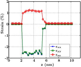
In Fig. 1 we show, following the approach by Pryor et al. Pryor et al. (1998), the strain tensor components , and along the axis ( axis) for one of the structures considered. The data shown here are averaged over the whole supercell. Several features are clearly visible. To a first approximation the different components reflect the profile one would expect from a continuum-based description. Caro et al. (2011) However, even when averaging the strain tensor components over the supercell, the impact of local alloy fluctuations giving rise to local strain tensor fluctuations is clearly visible. As we have seen already for random InGaN bulk systems, local strain field fluctuations significantly affect the valence and conduction band edges. Caro et al. (2013) Also the features arising from the WWFs are visible in the region of nm.
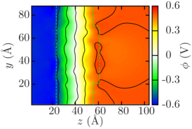
In a second step, we discuss the result from our local polarization theory. Figure 2 displays the calculated built-in potential for a slice through the center of the cylindrical-shaped WWF in the -plane for one of the considered structures. Again, the direction is parallel to the axis. As we can see from Fig. 2, the isolines inside the QW are not straight lines. This is in contrast to a continuum-based description. In our atomistic approach, the isolines are affected by the local strain and alloy fluctuations. In addition, the shape of the built-in potential is significantly affected by the presence of the WWF.
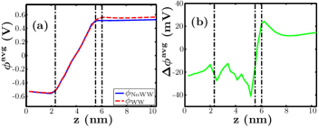
To further analyze the impact of WWFs on the built-in potential in -plane InGaN/GaN QWs, Fig. 3 (a) shows the built-in potential , averaged over the ten different configurations, for a line-scan through the QW along the axis. The line-scan runs through the center of the disklike WWF. reflects to a first approximation the capacitorlike behavior one would expect from a continuum-based description. The solid line shows the result in the absence of WWFs (), while the dashed line displays the built-in potential in the presence of WWFs (). The vertical dashed-dotted lines indicate the QW interfaces along the axis.
To analyze the impact of alloy and WWFs on the built-in potential in more detail, Fig. 3 (b) depicts . From this we can conclude two things. Firstly, even when averaging over the ten configurations the influence of the alloy fluctuations on built-in potential is clearly visible since is clearly not smooth in the QW region. Secondly, WWFs lead to a reduced built-in field inside the InGaN/GaN QW and near the upper interface. The change in the slope of inside the QW leads to the effect that the electron wave function can leak further into the QW center. The origin of the built-in field reduction can be explained using linear continuum elasticity theory. In this approach, the total built-in potential is the sum of the potential arising from the QW plus a contribution arising from a disk-shaped QD. By looking at Fig. 3 (b), the profile of reflects the characteristic of nitride-based QDs. Schulz and O’Reilly (2011)
III.2 Single-particle properties
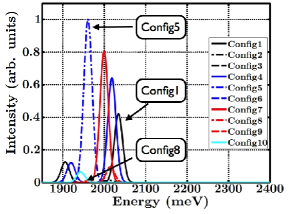
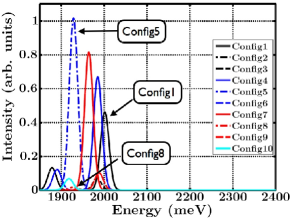
Figure 4 shows the ground-state emission spectrum without Coulomb interaction for ten different random configurations. The intensities are all normalized to the maximum intensity of configuration 5 (Config5). Several interesting features are clearly visible in the spectra.
Firstly, when looking at Fig. 4, we observe that different microscopic configurations give significantly different transition energies. This can also be seen from Table 1, where the single-particle transition energies are summarized. Without Coulomb effects, the difference between the lowest (Config3) and the highest (Config1) transition energy is 128.7 meV.
Secondly, a striking observation is that six out of ten configurations have an oscillator strength of less than 20% of the oscillator strength of configuration 5 (Config5). This indicates a weaker spatial wave function overlap of ground-state electron and hole levels. The main contribution to the emission spectrum arises here from the configurations 1, 4, 5, and 7. But even these four configurations have a spread of 73.7 meV in their transition energies.
| Config. | (eV) | (eV) | (meV) |
|---|---|---|---|
| 1 | 2.0344 | 2.0017 | 32.7 |
| 2 | 2.0119 | 1.9835 | 28.4 |
| 3 | 1.9057 | 1.8789 | 26.8 |
| 4 | 2.0184 | 1.9850 | 33.4 |
| 5 | 1.9607 | 1.9289 | 31.8 |
| 6 | 1.9198 | 1.8905 | 29.3 |
| 7 | 1.9997 | 1.9642 | 35.5 |
| 8 | 1.9560 | 1.9295 | 26.5 |
| 9 | 2.0149 | 1.9881 | 26.8 |
| 10 | 1.9431 | 1.9182 | 24.9 |
| Average | 1.9765 | 1.9469 | 29.6 |
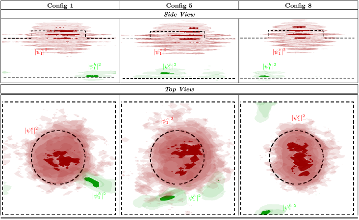
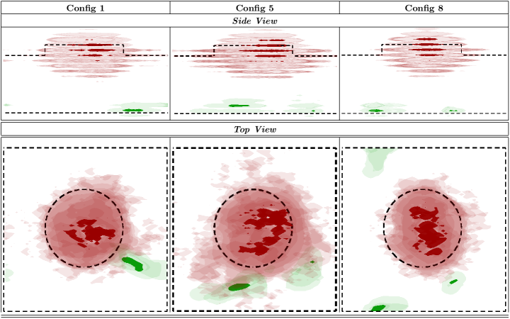
The broadening of the PL peak is usually attributed to wave function localization effects. To gain insight into the microscopic origin of such wave function localization effects and to elucidate the difference between different microscopic configurations, Fig. 5 shows the calculated single-particle electron and hole ground-state charge densities and , respectively, for Config1, Config5, and Config8. The charge densities for electrons (holes) are shown in red (green). A top view ( axis) and a side view ( axis) are given. The dashed lines indicate approximately the QW interfaces. The dark isosurfaces correspond to 50 % of the maximum value of the charge density, while the light isosurfaces correspond to 5% of the maximum value. Based on Fig. 4, these configurations have been chosen to represent the situation of a configuration with (i) a very large oscillator strength (Config 5), (ii) a very low oscillator strength (Config 8), and (iii) a system (Config 1) that can be regarded as an intermediate situation between (i) and (ii).
These charge density plots have several features in common. Firstly, the strong electrostatic built-in field leads to a spatial separation of electron and hole wave functions along the axis. However, and in contrast to standard continuum-based descriptions, which treat InGaN/GaN QWs as homogenous structures described by average parameters, we find a very strong (nm scale) hole wave function localization. Our results indicate therefore that already a random alloy is sufficient to lead to strong hole wave function localization effects. The electron wave functions are mainly localized by the presence of the WWF and show a larger localization length. It should also be noted that the electron wave functions are affected by local effects, since the charge density does not display a circular symmetry within the WWF. The localization length is here, to a first approximation, given by the dimensions of the WWF. The difference in the observed localization behavior can be attributed to the much higher hole effective mass compared to the electron effective mass. Rinke et al. (2008) Thus a much stronger hole wave function localization could be expected, consistent with our calculations. Our findings are in agreement with the results reported in Ref. Watson-Parris et al., 2011 for the hole states, but show that the electron charge density is also impacted by alloy fluctuation effects. Additionally, both electron and hole charge densities reflect the anion-cation structure of the underlying WZ lattice, with hole (electron) states preferentially located at anion (cation) planes/sites.
There are also differences clearly visible between the chosen configurations. In contrast to configurations 1 and 5, the hole wave function in configuration 8 is localized far away from the well width fluctuation (localization region of the electron) in and perpendicular to the plane. Consequently, one is left with a very weak spatial overlap and thus a very low oscillator strength. Configurations 1 and 5, however, are very similar with the hole wave function localizing near the WWF in the plane. However, configuration 5 seems to have a slightly higher overlap in the plane in comparison with configuration 1. This observation is also reflected in the transition strength displayed in Fig. 4.
| Orbital Contribution (%) | ||||||||
| Hole | Electron | |||||||
| Ground State | Ground State | |||||||
| Config. | ||||||||
| 1 | 82.29 | 15.73 | 1.63 | 0.35 | 1.15 | 1.10 | 4.57 | 93.18 |
| 2 | 75.67 | 20.85 | 2.82 | 0.66 | 0.67 | 0.85 | 4.46 | 94.02 |
| 3 | 27.19 | 69.48 | 2.69 | 0.64 | 0.88 | 1.07 | 4.79 | 93.26 |
| 4 | 85.90 | 10.98 | 2.50 | 0.62 | 1.28 | 1.35 | 4.66 | 92.71 |
| 5 | 73.55 | 24.49 | 1.60 | 0.36 | 1.04 | 1.03 | 4.63 | 93.29 |
| 6 | 17.33 | 79.36 | 2.66 | 0.65 | 1.05 | 1.11 | 4.68 | 93.16 |
| 7 | 87.83 | 9.35 | 2.26 | 0.56 | 0.88 | 0.91 | 4.61 | 93.60 |
| 8 | 41.63 | 55.19 | 2.55 | 0.63 | 1.54 | 1.19 | 4.75 | 92.52 |
| 9 | 14.71 | 83.02 | 1.76 | 0.51 | 1.09 | 0.89 | 4.66 | 93.36 |
| 10 | 22.66 | 74.82 | 2.00 | 0.51 | 1.17 | 0.95 | 4.74 | 93.14 |
| Average | 52.88 | 44.33 | 2.25 | 0.55 | 1.08 | 1.05 | 4.66 | 93.22 |
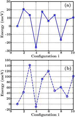
Having discussed that electron and hole wave functions are strongly localized for different reasons, we focus in the next step on the variation of the electron and hole ground-state energies between different configurations. This analysis reveals which of the two carrier types determines the variation in the transition energies shown in Fig. 4. The variation of the electron and hole ground state energies is displayed in Fig. 6 (a) and (b), respectively. Here the energies are calculated with respect to the ground-state energy of configuration 1 (). When looking at Fig. 6, in terms of its energy, configuration 1 seems to be an average configuration for the electrons. For the holes, it is a more extreme case, since the energy difference is most of the times very large. More specifically, we find that the electron energies vary in the range of 2-45 meV, while the hole ground state energies for different microscopic configurations scatter between 10 and 150 meV. For , the standard deviation is meV. For the holes, we find meV. This reflects the much stronger dependence of the hole ground-state energies on the specific microscopic random alloy configuration. However, it should be noted that we have considered here a specific size and shape for the WWF. To shed more light on the impact of WWFs on , we have performed calculations without WWFs. Since the hole states are localized by the random alloy fluctuations, when removing the WWF, the spread in is similar to the situation with WWFs. However, the interband transition energies are modified when we exclude WWFs. This arises from the fact that the electrons are now effectively localized in a narrower well, with a reduced potential drop across the well, as illustrated in Fig. 3, where the total potential drop is calculated to decrease by about 40 meV when the WWFs are removed. The distribution of WWF sizes and heights in actual samples should therefore also contribute to the experimentally observed broadening of InGaN QW absorption and emission spectra. A full treatment of the influence of WWFs on the transition energy would require a range of calculations, taking account both of variations in WWF sizes and also of the general reduction in electron-hole overlap with increasing well width and potential drop. This is beyond the scope of the present study. We can, however, conclude that random alloy fluctuations predominantly affect the hole ground-state energies, with WWFs affecting the electrons states, and with both factors then contributing to the overall broadening of the experimental absorption and emission spectra.
In addition, since our analysis reveals that local alloy effects significantly modify the valence band structure, we study in a further step the orbital character of electron and hole ground states. This analysis is important when investigating the optical polarization characteristic of InGaN/GaN QWs. This study goes beyond the capabilities of a single-band effective mass approximation. We note that with standard continuum-based approaches, which treat -plane InGaN QWs as homogenous structures described by average parameters, the topmost valence state would have a charge density, independent of the In content, with 50% - and 50% -like character. Table 2 shows the contributions of the , , , and orbitals to the hole and electron ground state on average and for the different configurations. The dominant orbital contribution in each configuration is highlighted. The electron ground state shows the expected behavior that the wave function is mainly given by -orbital contributions with much weaker contributions and negligible and character. For the hole ground state we observe strong variations in the - and -like orbital contributions. The fluctuations in these quantities can be attributed to local strain effects, explicitly taken into account in our model. However, on average our result is similar to the result expected from a multiband continuumlike description.
So far, we have focused our attention on ground-state properties. Since excited states make also a significant contribution to the optical properties, e.g. when describing the “S-shape” of the temperature dependence of the PL peak energies, Wang et al. (2012); Hammersley et al. (2012) we turn now to discuss excited states.
III.2.1 Excited states
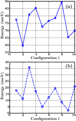
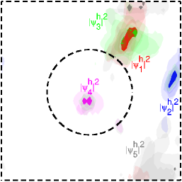
In a first step we look at the energetic separation and , respectively, of the ground state (GS) and the first excited (FE) state for electrons and also for holes as a function of the configuration . Figure 7 (a) shows , while Fig. 7 (b) depicts . From this figure one can infer again a strong difference between the results for the electrons and the holes. For the electrons scatters between 60-90 meV, while varies from 3-35 meV. The calculated mean value for electrons is meV and for holes meV. The calculated standard deviations meV and meV are very similar. However, when looking at , we find a much smaller value for electrons () than for holes (). This difference can be related to the difference in the impact of local alloy fluctuations and QW confinement effects on the electronic structure. We have already seen that the hole wave functions are significantly affected by local alloy fluctuations, while the electron wave functions, to a first approximation are localized by the WWFs. As discussed above, this difference arises from the difference in the effective masses. Therefore, the electrons are mainly affected by the overall confinement potential of the QW. Given the low electron effective mass, compared to the holes, a large splitting between ground and first excited electron state can be expected. The hole wave functions, due to their high effective mass, however, can localize in different potential minima/maxima originating from alloy fluctuations. This means that not only the hole ground state is expected to be highly localized but also excited states. To confirm this we have calculated the charge densities of the first five hole states for a given random supercell. As an example we have chosen configuration 1 (Config1) here, and the results are depicted in Fig. 8. One can clearly see that not only the hole ground state () reveals a strong localization but also the shown excited states. This behavior is not a particularity of configuration 1, all the other configurations show a similar behavior. The presence of localized excited states is consistent with the experimental observation of the “S-shape” temperature dependence in the PL spectra of InGaN/GaN QWs.
All the above highlighted factors shed further light on the features observed in the calculated emission spectrum [cf. Fig. 4]. The presence of the strong built-in field combined with the strong hole wave function localization, arising from local alloy fluctuations, and the electron wave function localization due to WWFs leads to small wave function overlaps of electron and hole ground states. Thus, the ground-state electrons and holes are likely to be localized at spatially separated positions in and perpendicular to the plane. This explains that the ground state transition strength in six out of ten configurations is weak. It should be noted that therefore a QD-like description of random alloy fluctuations in a continuum-based model might fail, since it does not account for the effect that the charge carriers are likely to be localized in different in-plane spatial positions.
So far, we have not taken into account Coulomb effects, which could increase the spatial overlap of electron and hole wave functions by compensating localization and built-in potential effects. Thus, we focus on the impact of Coulomb effects on the results in the next section.
III.3 Coulomb effects
To include Coulomb effects in the description, we use the CI scheme described in Sec. I.3. Since we have seen in the previous section that the energetic separation between different hole states is small, we include the first 15 hole states in the CI expansion. For the electrons we include the five energetically lowest single-particle states.
Figure 9 shows the calculated excitonic ground-state emission spectrum for the here considered ten different random configurations. The intensities are all normalized to the maximum intensity of configuration 5 without Coulomb effects [cf. Fig. 4]. Compared to Fig. 4, the (attractive) Coulomb interaction seems to introduce mainly an energetic shift of the whole emission spectrum. When including Coulomb effects the oscillator strength is, for the different transitions, only slightly increased. This indicates that the spatial separation of the electron and hole wave functions due to the presence of built-in potential and localization effects is much stronger than the attractive Coulomb interaction between the carriers. Similar to the situation without Coulomb effects we observe that different microscopic configurations give significantly different transition energies. The excitonic transition energies are summarized in Table 1. With Coulomb effects the difference between the lowest (Config3) and the highest (Config1) transition energy is 122.8 meV, which is only slightly different to the result in the absence of the Coulomb interaction (128.7 meV).
Also, Table 1 summarizes the calculated excitonic shifts for the different configurations. On average we find a shift of 29.6 meV, corresponding to the exciton binding energy. Recently, Wei and co-workers Wei et al. (2012) analyzed the excitonic binding energy in the framework of a single-band effective mass description, but neglecting alloy or well-width fluctuations. The authors find an excitonic binding energy of approximately 25 meV for a 3.5 nm wide N/GaN QW. The continuum based calculations by Funato and Kawakami, Funato and Kawakami (2008) give for an N/GaN QW with 3 nm width approximately 23 meV. However, these continuum-based QW calculations neglect the effect of in-plane carrier localization due to alloy fluctuations or WWFs. Such an in-plane confinement would increase the in-plane wave function overlap and consequently leads to an increase of the excitonic binding energy. As discussed before, the single-particle wave functions, as shown in Fig. 4, reveal not only a strong confinement along the -axis but also in-plane. While for configurations 1 and 5 electron and hole wave functions are almost localized at the same in-plane position, in configuration 8 they are not. This is also reflected in the excitonic binding energies. Configurations 1 and 5 have almost identical excitonic binding energies (32.7 meV versus 31.8 meV), while for configuration 8 the excitonic binding energy is much smaller (26.5 meV).
Funato and Kawakami Funato and Kawakami (2008) calculated also the excitonic binding energies of cylindrical InGaN/GaN QDs, therefore including lateral confinement effects. In the case of a cylindrical InGaN/GaN QD with a height of 3 nm and a diameter of 6 nm, the excitonic binding energies were increased, compared to a QW with an identical height and composition, by approximately 13 meV. For 25 % In, this gives approximately an excitonic binding energy of 36 meV. This value is comparable to our average excitonic binding energy of 29.6 meV, which also includes, due to alloy and WWFs, lateral confinement effects.
Having discussed the impact of Coulomb effects on the emission spectrum, we focus in the next step on the impact of the Coulomb interaction on the charge densities. In the CI scheme the excitonic many-body wave function is not a simple product of electron and hole wave functions, but it is written as a linear combination of electron-hole basis states:
| (7) |
Here, is the vacuum state, the expansion coefficient and () denotes the electron (hole) creation operator. Barthel et al. (2013) To visualize the electron and hole contribution to separately we use a reduced density matrix for electrons and holes. Barthel et al. (2013) For the electrons, the density operator is given by:
| (8) |
One can now calculate the electron and hole densities and , respectively. Following Fig. 5, Fig. 10 depicts the calculated electron [] and hole [] densities for the configurations 1, 5, and 8. When comparing Figs. 5 and 10, we infer that the position of the charge densities along the axis are only slightly affected by the Coulomb interaction for the here considered N/GaN QW. This shows that the spatial separation of the charge carriers is dominated by the built-in field, explaining that the oscillator strength is only very slightly modified by the attractive Coulomb interaction [cf. Fig. 4]. This situation could change with decreasing In content due to reduced built-in fields.
Similar to the effect along the axis, we find that electron and hole charge densities are only slightly modified by the Coulomb interaction in the plane. Based on the above effective mass argument, one could expect that the hole state is less affected by the Coulomb interaction, and that the electron wave function mainly changes and localizes near the hole. All the displayed configurations show that localization effects due to random alloy and well-width fluctuations are stronger than Coulomb effects. Only slight effects in the shape of the electron and hole wave functions are visible.
IV Comparison with experimental data
Our finding of localization effects on the nanometer scale is in good agreement with the experimental analysis by Graham et al. Graham et al. (2005) Graham and co-workers used the Huang-Rhys factor to analyze the localization length for the carriers in InGaN/GaN QWs. For varying In content, the authors estimated localization lengths of 1.1-3.1 nm. Graham et al. (2005) Our results are consistent with these experimental findings. However, Graham et al. assumed that the localization length is the same for electrons and holes. Our results reveal that the experimentally estimated localization length is consistent with the hole wave function localization, since the localization length of the electrons will be mainly determined by the size of in-plane WWFs, at least for the here considered 25% InN system. It should also be noted that we have studied here the lower limit (5 nm) of the experimentally reported values (5-10 nm). Galtrey et al. (2008) Thus, one could expect that when increasing the in-plane dimension of the WWFs, the localization length of the electrons is of the order 5-10 nm.
Next, we compare our calculated excitonic transition energies with available experimental data and analyze also the emission spectrum in terms of the experimentally available data on the full width half maximum (FWHM) of the PL peak. Here we have only a small number of different microscopic random alloy configurations. Thus, a detailed comparison is difficult. However, the present analysis allows us to study if our approach gives numbers of the right order of magnitude. For the here studied 3.5 nm wide N/GaN QW, we estimate an average excitonic transition energy of 1.95 eV [cf. Table 1]. Graham et al. Graham et al. (2005) extracted for a 3.3 nm wide N/GaN QW a PL peak energy of 2.162 eV, which is in good agreement with our calculations, given that our well is slightly wider and that we neglect also electron-phonon coupling effects.
We have also seen in Sec. III.3, that the main contribution to the calculated excitonic emission spectrum (cf. Fig. 9) arise from the configurations 1, 4, 5, and 7. The ground-state emission energy for those configurations is spread over a range of 72.8 meV. This value can now be compared to the experimental study of the FWHM of the PL peak in Ref. Graham et al., 2005 (cf. Ref. Watson-Parris et al., 2011). The experimental data for a 3.3 nm wide N/GaN QW gives a FWHM of about 63 meV.
As discussed above, for a more detailed comparison with experimentally available data, the analysis of more microscopic structures, different well width, WWFs and In contents would be required. This is beyond the scope of the present study, since we are here interested in the discussion of the general features of -plane InGaN/GaN QWs when taking alloy and WWFs explicitly into account. Nevertheless, our first results for the localization length, excitonic transition energies and their energetic variation give already values in very reasonable agreement with those reported in literature experimental studies.
V Conclusion
In conclusion, we have presented an atomistic approach, including local alloy, well-width, strain and built-in field fluctuations, to analyze the electronic and optical properties of -plane N/GaN QWs. Our calculations show that random alloy fluctuations lead to a very strong hole wave function localization (on the nm scale) which affects the QW optical properties significantly. The observed hole wave function localization is consistent with the experimentally estimated localization lengths of 1-3 nm. Graham et al. (2005) Additionally, we find that the electron wave functions are mainly localized by WWFs, with some contributions from the local alloy fluctuations. Moreover, by treating the optical properties in the CI frame, we were able to show that the emission spectra is dominated by the localized single-particle states due to well-width and alloy fluctuations and that the Coulomb interaction mainly affects the carrier wave functions in the growth plane and leads to overall energetic shifts of the emission spectrum. However, it should be noted that this behavior could be significantly different for systems with low In content or structures grown on non- or semi-polar planes. These systems will be analyzed in future studies.
Acknowledgements.
The authors would like to thank Philip Dawson, Rachel A. Oliver, Menno Kappers and Colin J. Humphreys for fruitful discussions. This work was supported by Science Foundation Ireland (project numbers 10/IN.1/I2994 and 13/SIRG/2210) and the European Union 7th Framework Programme DEEPEN (grant agreement no.: 604416).References
- Humphreys (2008) C. J. Humphreys, MRS Bulletin 33, 459 (2008).
- Nakamura (1998) S. Nakamura, Science 281, 956 (1998).
- Oliver et al. (2010) R. A. Oliver, S. E. Bennett, T. Zhu, D. J. Beesley, M. J. Kappers, D. W. Saxey, A. Cerezo, and C. J. Humphreys, J. Phys. D: Appl. Phys. 43, 354003 (2010).
- Chichibu et al. (2006) S. F. Chichibu, A. Uedono, T. Onuma, B. A. Haskell, A. Chakraborty, T. Koyama, P. T. Fini, S. Keller, S. P. DenBaars, J. S. Speck, et al., Nature Mater. 5, 810 (2006).
- Schöming et al. (2004) H. Schöming, S. Halm, A. Forchel, G. Bacher, J. Off, and F. Scholz, Phys. Rev. Lett. 92, 106802 (2004).
- Wang et al. (2012) H. Wang, Z. Ji, S. Qu, G. Wang, Y. Jiang, B. Liu, X. Xu, and H. Mino, Optics Express 20, 3932 (2012).
- Hammersley et al. (2012) S. Hammersley, D. Watson-Parris, P. Dawson, M. J. Godfrey, T. J. Badcock, M. J. Kappers, C. McAleese, R. A. Oliver, and C. J. Humphreys, J. Appl. Phys. 111, 083512 (2012).
- Bernardini et al. (1997) F. Bernardini, V. Fiorentini, and D. Vanderbilt, Phys. Rev. B 56, R10024 (1997).
- Lee and Wang (2006) B. Lee and L. W. Wang, J. Appl. Phys. 100, 093717 (2006).
- Wu et al. (2009) X. Wu, E. J. Walter, A. M. Rappe, R. Car, and A. Selloni, Phys. Rev. B 80, 115201 (2009).
- Chan et al. (2010) J. A. Chan, J. Z. Liu, and A. Zunger, Phys. Rev. B 82, 045112 (2010).
- Gorczyca et al. (2009) I. Gorczyca, S. P. Lepkowski, T. Suski, N. E. Christensen, and A. Svane, Phys. Rev. B 80, 075202 (2009).
- Liu et al. (2010) Q. Liu, J. Lu, Z. Gao, L. Lai, R. Qin, H. Li, J. Zhou, and G. Li, Phys. Stat. Sol B 247, 109 (2010).
- Moses et al. (2011) P. G. Moses, M. Miao, Q. Yan, and C. G. Van de Walle, J. Chem. Phys. 134, 084703 (2011).
- Pela et al. (2011) R. R. Pela, C. Caetano, M. Marques, L. G. Ferreira, J. Furthmüller, and L. K. Teles, Appl. Phys. Lett. 98, 151907 (2011).
- Funato and Kawakami (2008) M. Funato and Y. Kawakami, J. Appl. Phys. 103, 093501 (2008).
- Watson-Parris et al. (2011) D. Watson-Parris, M. J. Godfrey, P. Dawson, R. A. Oliver, M. J. Galtrey, M. J. Kappers, and C. J. Humphreys, Phys. Rev. B 83, 115321 (2011).
- Yang et al. (2014) T.-J. Yang, R. Shivaraman, J. S. Speck, and Y.-R. Wu, J. Appl. Phys. 116, 113104 (2014).
- Schulz et al. (2013) S. Schulz, M. A. Caro, L.-T. Tan, P. J. Parbrook, R. W. Martin, and E. P. O’Reilly, Appl. Phys. Express 6, 121001 (2013).
- Caro et al. (2013) M. A. Caro, S. Schulz, and E. P. O’Reilly, Phys. Rev. B 88, 214103 (2013).
- Musgrave and Pople (1962) M. J. P. Musgrave and J. A. Pople, Proc. R. Soc. Lond. A 268, 474 (1962).
- Keating (1966) P. N. Keating, Phys. Rev. 145, 637 (1966).
- Martin (1970) R. M. Martin, Phys. Rev. B 1, 4005 (1970).
- Gale and Rohl (2003) J. D. Gale and A. L. Rohl, Molecular Simulation 29, 291 (2003).
- O’Reilly et al. (2002) E. P. O’Reilly, A. Lindsay, S. Tomic, and M. Kamal-Saadi, Semicond. Sci. Technol. 17, 870 (2002).
- Li and Pötz (1992) Z. Q. Li and W. Pötz, Phys. Rev. B 46, 2109 (1992).
- Boykin et al. (2007) T. B. Boykin, N. Kharche, G. Klimeck, and M. Korkusinski, J. Phys.: Condens. Matter 19, 036203 (2007).
- Jancu et al. (1998) J. M. Jancu, R. Scholz, F. Beltram, and F. Bassani, Phys. Rev. B 57, 6493 (1998).
- Boykin et al. (2002) T. B. Boykin, G. Klimeck, R. C. Bowen, and F. Oyafuso, Phys. Rev. B 66, 125207 (2002).
- Winkelnkemper et al. (2006) M. Winkelnkemper, A. Schliwa, and D. Bimberg, Phys. Rev. B 74, 155322 (2006).
- Schulz et al. (2010) S. Schulz, T. J. Badcock, M. A. Moram, P. Dawson, M. J. Kappers, C. J. Humphreys, and E. P. O’Reilly, Phys. Rev. B 82, 125318 (2010).
- Yan et al. (2009) Q. Yan, P. Rinke, M. Scheffler, and C. G. Van de Walle, Appl. Phys. Lett. 95, 121111 (2009).
- Ranjan et al. (2003) V. Ranjan, G. Allan, C. Priester, and C. Delerue, Physical Review B 68, 115305 (2003).
- Saito and Arakawa (2002) T. Saito and Y. Arakawa, Physica E (Amsterdam) 15, 169 (2002).
- Zielinski et al. (2005) M. Zielinski, W. Jaskolski, J. Aizpurua, and G. W. Bryant, Acta Physica Polonica A 108, 929 (2005).
- Schuh et al. (2012) K. Schuh, S. Barthel, O. Marquardt, T. Hickel, J. Neugebauer, G. Czycholl, and F. Jahnke, Appl. Phys. Lett. 100, 092103 (2012).
- Sheng et al. (2005) W. Sheng, S. J. Cheng, and P. Hawrylak, Phys. Rev. B 71, 035316 (2005).
- Schulz et al. (2006) S. Schulz, S. Schumacher, and G. Czycholl, Phys. Rev. B 73, 245327 (2006).
- Ziemann and May (2014) D. Ziemann and V. May, J. Phys. Chem. Lett. 5, 1203 (2014).
- Schnell et al. (2002) I. Schnell, G. Czycholl, and R. C. Albers, Phys. Rev. B 65, 075103 (2002).
- Lee et al. (2001) S. Lee, L. Jönsson, J. W. Wilkins, G. W. Bryant, and G. Klimeck, Phys. Rev. B 63, 195318 (2001).
- Barenco and Dupertuis (1995) A. Barenco and M. A. Dupertuis, Phys. Rev. B 52, 2766 (1995).
- Franceschetti et al. (1999) A. Franceschetti, H. Fu, L. W. Wang, and A. Zunger, Phys. Rev. B 60, 1819 (1999).
- Baer et al. (2004) N. Baer, P. Gartner, and F. Jahnke, Eur. Phys. J. B 42, 231 (2004).
- Graham et al. (2005) D. M. Graham, A. Soltani-Vala, P. Dawson, M. J. Godfrey, T. M. Smeeton, J. S. Barnard, M. J. Kappers, C. J. Humphreys, and E. J. Thrush, J. Appl. Phys. 97, 103508 (2005).
- Monemar et al. (2002) B. Monemar, P. P.Paskov, J. P. Bergman, G. Pozina, V. Darakchieva, M. Iwaya, S. Kamiyama, H. Amano, and I. Akasaki, MRS Internet J. Nitride Semicond. Res. 7, 7 (2002).
- Smeeton et al. (2003) T. M. Smeeton, M. J. Kappers, J. S. Barnard, M. E. Vickers, and C. J. Humphreys, Appl. Phys. Lett. 83, 5419 (2003).
- Galtrey et al. (2007) M. J. Galtrey, R. A. Oliver, M. J. Kappers, C. J. Humphreys, D. J. Stokes, P. H. Clifton, and A. Cerezo, Appl. Phys. Lett. 90, 061903 (2007).
- Galtrey et al. (2008) M. J. Galtrey, R. A. Oliver, M. J. Kappers, C. J. Humphreys, P. Clifton, D. Larson, D. Saxey, and A. Cerezo, J. Appl. Phys. 104, 013524 (2008).
- Bennett et al. (2011) S. E. Bennett, D. W. Saxey, M. J. Kappers, J. S. Barnard, C. J. Humphreys, G. D. W. Smith, and R. A. Oliver, Appl. Phys. Lett. 99, 021906 (2011).
- Baloch et al. (2013) K. H. Baloch, A. C. Johnston-Peck, K. Kisslinger, E. A. Stach, and S. Gradecak, Appl. Phys. Lett. 102, 191910 (2013).
- Moram and Vickers (2009) M. A. Moram and M. E. Vickers, Rep. Prog. Phys. 72, 036502 (2009).
- Pryor et al. (1998) C. Pryor, J. Kim, L. W. Wang, A. J. Williamson, and A. Zunger, J. Appl. Phys. 83, 2548 (1998).
- Caro et al. (2011) M. A. Caro, S. Schulz, S. B. Healy, and E. P. O’Reilly, J. Appl. Phys. 109, 084110 (2011).
- Schulz and O’Reilly (2011) S. Schulz and E. P. O’Reilly, Phys. Status Solidi A 208, 1551 (2011).
- Rinke et al. (2008) P. Rinke, M. Winkelnkemper, A. Qteish, D. Bimberg, J. Neugebauer, and M. Scheffler, Phys. Rev. B 77, 075202 (2008).
- Wei et al. (2012) S. Wei, Y. Jia, and C. Xia, Superlattices and Microstructures 51, 9 (2012).
- Barthel et al. (2013) S. Barthel, K. Schuh, O. Marquardt, T. Hickel, J. Neugebauer, F. Jahnke, and G. Czycholl, Eur. Phys. J. B 86, 449 (2013).