Comment on “Reducing error rates in straintronic multiferroic nanomagnetic logic by pulse shaping” [Nanotechnology 26, 245202 (2015)]
In Ref. 1, the authors proposed to reduce error probability of switching in a system of two dipole-coupled magnetostrictive nanomagnets in strain-mediated multiferroic heterostructures using voltage (stress) pulse shaping. The authors conclude that high success probability of switching cannot be achieved at high switching speed (1 ns), and therefore their proposed system is only applicable for niche applications. However, such conclusion lacked the critical understandings behind such high error probability for general-purpose logic applications. Fortunately, such analysis and a possible solution along the line of the analysis is present in literature [2] using Bennett clocking [3] for logic design, on which Ref. 1 (and arXiv version Ref. 4) has made some incorrect statements. Earlier, a subset of the authors of Ref. 1 also published a paper [5] on a four magnet system using the Bennett clocking mechanism, where the authors also came up with a similar conclusion of high error probability and the demise of multiferroic nanomagnetic logic, however, without relevant analysis similar to the case as in the Ref. 1.
First, the Fig. 1 in Ref. 1 shows the directions of unit vectors in standard Cartesian coordinate system (--) incorrectly (one correct option is to interchange and ), and also the demagnetization factors in the Equations (7), (8), and (9) are incorrect. This may have produced incorrect results in the paper [1]. In any case, a correct coordinate system will be utilized in this Comment as shown in Fig. 1(a).
The Fig. 2(c) in Ref. 1 concerns about the in-plane potential landscape of the nanomagnets to analyze the error probability, however, the critical analysis in Ref. 2 has shown that it is the out-of-plane motion that is responsible for high error probability and a solution along the line of such critical analysis was presented. The intriguing dynamics of a complete switching for a single magnetostrictive nanomagnet has been studied elaborately in Refs. 6, 7. The torque due to stress acts in the out-of-plane ( in Fig. 1) direction as
where is the potential energy due to stress per unit volume, is the magnetostrictive coefficient, and is the stress. If such out-of-plane motion is not considered, the complete motion cannot be possible [6, 7]. Also such switching is confirmed by others [8, 9, 10]. Such out-of-plane motion also increases the switching speed to the order of GHz [6, 7].
Ref. 11 incorrectly assumed only in-plane motion of magnetization for logic design using Bennett clocking, and the switching delay of magnetization according to Ref. 11 is 1000 ns, and that is clearly untenable for building general purpose nanoelectronics [12, 13]. Fortunately, the analysis in Ref. 11 is incorrect and it was corrected by Roy for memory design [14, 15, 16, 6, 17, 7] and also for logic design [14, 18, 19]. Similarly, in the presence of thermal fluctuations, the critical analysis due to out-of-plane excursion of magnetization is missing in Refs. 1, 4, 5 for logic design purposes with wrong conclusions of high switching delay and high error probability; correct analysis has been performed by Roy in Ref. 2. Such out-of-plane motion also plays important role in determining the pertinent energy dissipation [20, 21, 22].
-
1.
Ref. 1 states while referring Ref. 2 that “it examined switching errors in straintronic memory (not logic)”. This is preposterous since Fig. 1(b) in Ref. 2 clearly shows the logic design using Bennett clocking for four-nanomagnet system and the underlying equations are also derived and provided. Actually, Ref. 1 analyzed only two nanomagnet system, therefore, the system in Ref. 1 is incomplete to be termed as logic design.
-
2.
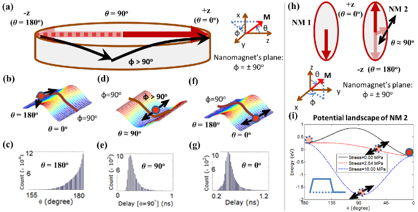
Ref. 1 states while referring Ref. 2 that “A feedback circuit will determine when the magnetization has rotated by … at that juncture.” This has been already stated and explained in literature [6, 7] and Ref. 1 stated it quite inaccurately. Fig. 1(a) shows that magnetization gets deflected out-of-plane due to the torque exerted on it [see Equation (Comment on “Reducing error rates in straintronic multiferroic nanomagnetic logic by pulse shaping” [Nanotechnology 26, 245202 (2015)])]. The three-dimensional potential landscapes are also shown in the Figs. 1(b), (d), (f), depicting the out-of-plane motion of magnetization. Due to thermal fluctuations, the initial angle distribution of magnetization [Fig. 1(c)] and the time it takes to reach is a wide distribution [Fig. 1(e)]. Stress needs to be withdrawn when magnetization reaches around so that magnetization traverses towards [switching delay distribution is shown in Fig. 1(g)], and does not backtrack towards , causing switching failure [6, 7]. This is purely dynamical phenomenon [6, 7] contrary to stead-state analysis. Therefore, a sensing element is required to detect when magnetization reaches around [6, 7]. The sensing element can be a spin valve or magnetic tunnel junction (MTJ), which is required to read the magnetization state [6, 7, 23]. We can get calibrated on the magnetoresistance of the spin valve or MTJ when and comparing this known signal with the sensed signal of the MTJ, the stress can be ramped down [6, 7]. According to the study presented in Refs. 6, 7, note that there is tolerance around , i.e., stress does not need to be withdrawn precisely at the juncture (this was also incorrectly stated in Refs. 21, 24, 25).
Similarly, in a two nanomagnet system [1], or in a complete four nanomagnet system using Bennett clocking [2], the out-of-plane excursion of magnetization needs to be considered as depicted in the Fig. 1(h). If magnetization gets deflected in so-called bad -quadrants, as explained in Refs. 6, 7, 2, the dipole coupling from the nanomagnet 1 [Fig. 1(h)] is not sufficient to switch the nanomagnet 2 in the correct direction, causing error in logic design. Ref. 1 considers only in-plane potential landscape while explaining, therefore it could not explain the primary reason behind the high error probability in magnetization switching for logic design purposes.
It should be noted that it is possible to harness more asymmetry in the system, rather than depending only on the out-of-plane excursion of magnetization [6, 7, 2], so that the sensing procedure and dynamic withdrawal of stress will not be required. As shown in Ref. 26, the interface and exchange coupling can create asymmetry in the system facilitating non-toggle switching, without any requirement of the sensing procedure.
-
3.
Ref. 1 uses a vague term ‘interactive pulse timing’ regarding Ref. 2. As explained in the above point, the strategy proposed in Ref. 2 is in line to the physical operation of the basic device operation, which Ref. 1 could not conceive. The pulse shaping methodology proposed in Ref. 1 is based on the understanding of in-plane motion and not on out-of-plane motion. Only in the very end of the paper, it vaguely states that “provided the out-of-plane magnetization effects do not begin to dominate first.” As explained in the above point, the contents in Ref. 1 lack the key understandings and analysis behind the critical device operation and high error probability.
-
4.
Ref. 1 states while referring Ref. 2 that “Unfortunately, the feedback circuit will dissipate so much energy that it defeats the very purpose of SML. It is therefore an ineffective countermeasure.” Actually, the research presented in Ref. 1 is an ineffective countermeasure since it concludes that low error probability cannot be achieved for logic design with their proposal, i.e., pulse shaping. Moreover, it could not analyze the reasoning behind high error probability, which nonetheless exists in the literature [2].
Ref. 1 foretell without any reasoning that the sensing element will dissipate too much energy. It appears that the authors in Ref. 1 think that logic is limited to four magnet systems [5] and it would require charge-based transistors to build any other circuitry [27, 28, 29, 30, 31]. Such thinking misses the big picture involved. Note that researchers are trying to replace the traditional transistors by a new possible energy-efficient switch (e.g., using multiferroic composites). Therefore, any required circuitry in general can be built with the energy-efficient switch itself rather than using charge-based transistors. Usually, it requires several peripheral circuitry in addition to the basic switch itself and it does not change the orders of energy dissipation [32, 33].
As stated in Refs. 6, 7, the sensing element to detect when magnetization reaches around can be implemented with spin valve or magnetic tunnel junction, which is anyway required to read the magnetization state of a nanomagnet [23]. And it is well-known that a small magnitude of current is required to read the magnetization state, leading to only miniscule energy dissipation. Therefore, the comment made by Ref. 1 is untenable.
A few contradicting facts vis-a-vis the comment made by Ref. 1 are pointed out below.
-
(a)
Ironically, a couple of authors in Ref. 1, Bandyopadhyay and Atulasimha (referred as BA onwards) are coauthors of Roy in Refs. 15, 16, 6, 17, 7. In particular, energy efficiency is claimed in the presence of thermal fluctuations in Ref. 17, which requires the sensing element too. Also, there is a patent [34] filed by BA including Roy’s contributions [15, 16, 6, 17, 7, 14, 18] claims energy-efficiency requiring the sensing element therein as well. Therefore, the comment made by Ref. 1 is very perplexing.
-
(b)
Note that Ref. 1 uses precisely shaped pulses. Such pulses need to be generated too using some circuitry. According to the perception of Ref. 1, transistors need to be utilized and the system would dissipate too much energy, invalidating the claim of energy efficiency in Ref. 1. Note that one additional hardware cannot be shared between many devices distributed on a chip due to interconnect delay and loading effect. Also, note that pulse shaping is an ineffective countermeasure since it is not helping much in reducing the error probability, therefore building and using such circuitry do not make sense.
-
(c)
Ref. 25, in which BA are coauthors, proposed a “toggle” switch (as stated that “a write cycle must be preceded by a read cycle to determine the stored bit”), which would require a similar use of spin-valve or MTJ for reading the known bit, storing it, and then using it for comparison. According to the perception of Ref. 1, such additional circuitry needs to be constructed with energy-inefficient transistors, invalidating the claim of energy efficiency in Ref. 25.
Fortunately, the perception in Ref. 1 is incorrect, otherwise, no system comprised of multiferroic devices would have been energy-efficient; transistors would have been required always to build the peripheral circuitry. Note that such sensing circuitry is not always required. It is shown in Ref. 26 that the interface and exchange coupling can create enough asymmetry in the system facilitating non-toggle switching, without any requirement of the sensing procedure and dynamic withdrawal of stress. Therefore, Ref. 1 misses several key understandings in this respect.
-
(a)
-
5.
Ref. 1 states while referring Ref. 2 that “We do not use any such construct and retain the energy advantage of SML.” First, note that Ref. 1 fails to achieve high switching speed at tolerable error probability for logic design. Ref. 1 does not mention that the proposal in Ref. 2 achieves high switching speed (1ns) at low error probability () for logic design. The pulse shaping methodology in Ref. 1 cannot tackle the critical issue behind switching failures as analyzed in Ref. 2.
Apart from making incorrect and misleading statements on Ref. 2, Ref. 1 is erroneous in the following aspects.
-
1.
Ref. 1 states that “Since our voltage pulse widths are 1 ns or more, we can neglect effects associated with finite rise and fall times of the stress in response to an abrupt voltage pulse.” Note that it is shown in literature [6, 7, 17] that particularly fall time is important to consider, since it may rotate magnetization out-of-plane in a direction that affects the error probability. Therefore, without a relevant analysis, the comparative basis of using different pulses (e.g., cases 3 and 4 pertain to ramped pulses, while the other cases do not) in Ref. 1 is untenable.
-
2.
Ref. 1 states that “Therefore, operating in the dipole dominated region reduces error rate but increases switching delay (because the stress is relatively weak), while operating at stress levels much above the dipole dominated region has the opposite effect.” The comment that “operating in the dipole dominated region reduces error rate” is incorrect, since the error occurs while withdrawing the stress. If the magnetization’s out-of-plane excursion is in so-called bad quadrant, it may be detrimental and magnetization may traverse in the opposite direction, as explained in Ref. 2. Therefore finite ramp rate particularly while withdrawing the stress is necessary to consider. Ref. 1 did not consider finite ramp rate, which is not only unphysical but also very important for relevant quantitative analysis. The dipole coupling makes the potential landscape asymmetric and the degree of asymmetry is same irrespective of stress, which is symmetric. Such statement fails to identify the key issue that dipole coupling makes small asymmetry in the system herein. This is why dipole coupling cannot counter the motion due to out-of-plane excursion, as explained in Ref. 2, and thereby Ref. 1 pertains to a high error probability.
Also, “operating at stress levels much above the dipole dominated region has the opposite effect.” is far from accurate since with high stress level accompanied by finite ramp rate, there can be considerable -motion [see Equation (Comment on “Reducing error rates in straintronic multiferroic nanomagnetic logic by pulse shaping” [Nanotechnology 26, 245202 (2015)])] and precession, increasing the switching delay eventually [6, 7, 17].
-
3.
While explaining the peak in Fig. 5, Ref. 1 says that with the increase of stress “the influence of dipole interaction is diminished” etc. This is not a correct explanation since asymmetric dipole coupling is always active alongwith the symmetric stress [see Fig. 1(i)]. For a correct explanation, one needs to invoke the out-of-plane excursion of magnetization with stress amplitude and stress pulse timing as parameters, as explained in Ref. 2.
-
4.
Ref. 1 states incorrectly that “Any combination of , and that gives a barrier height of 32 kT will yield similar results.” Note that the demagnetization factors dictate the magnetization dynamics and they depend on the specific values of , and . For example, switching delay can vary twice or more for the same barrier height [35]. This is a basic understanding regarding magnetization dynamics. Also, the barrier height needs to be calculated accurately. Several papers [21, 24, 25] underestimated the barrier height as much as by 40% using the assumption .
- 5.
-
6.
There are less serious but confusing and erroneous issues in Ref. 1, e.g., Equations (7)-(9) should have “” in stead of “” (sometimes is used for ), the calculated values of Equations (8) and (9) correspond to instead of , in Fig. 4, (instead of ) is used as azimuthal angle, there are two Fig. 4(c)s in the plot, Figs. 6, 8, and 10 plot from to , while has a range of only and it therefore depicts some duplicate and separated distributions incorrectly, also it appears that the last set in the Figs. 6, 8, 10 corresponds to 2 ns rather than 3 ns etc.
While there exists a litany of errors in Ref. 1, the purpose of this Comment is to primarily point out that Ref. 1 has made incorrect statements on Ref. 2 as explained earlier: (1) misquoted that Ref. 2 deals with memory and not logic, (2) did not mention that the proposal in Ref. 2 can keep the switching speed high 1 ns alongwith low error probability, unlike the case in Ref. 1, and (3) made misleading statement that energy dissipation in Ref. 2 is high. The understandings reflected in Ref. 1 are incorrect and not sound, while predicting the demise of multiferroic nanomagnetic logic in the presence of thermal fluctuations [1, 4, 5, 36, 37].
It should be also pointed out that there is issue with scaling down device dimensions since the analysis performed in Ref. 1 depends on the in-plane asymmetry created by dipole-coupling (between laterally placed nanomagnets), which decreases with scaling. Therefore, in the scaled-down nanomagnets, the error-probability would be even higher than what is mentioned in Ref. 1. There is also similar issue regarding area consumption on the proposals in Refs. 24, 25 due to using lateral piezoelectric pads, which is tantamount to micro-electronics rather than nano-electronics [12, 13], and therefore untenable for meeting practical standard requirement of area density 1 Tb/in2. Both theoretical and experimental works are emerging in this area [38] and the issues pointed out here hopefully would play an important role in devising memory and logic in our future information processing systems.
References
References
- [1] Munira K, Xie Y, Nadri S, Forgues M B, Fashami M S, Atulasimha J, Bandyopadhyay S and Ghosh A W 2015 Nanotechnology 26 245202
- [2] Roy K 2014 Appl. Phys. Lett. 104 013103
- [3] Bennett C H 1982 Int. J. Theor. Phys. 21 905–940
- [4] Munira K, Xie Y, Nadri S, Forgues M B, Fashami M S, Atulasimha J, Bandyopadhyay S and Ghosh A W 2014 arXiv1405.4000v1
- [5] Fashami M S, Munira K, Bandyopadhyay S, Ghosh A W and Atulasimha J 2013 IEEE Trans. Nanotechnol. 12 1206–1212
- [6] Roy K, Bandyopadhyay S and Atulasimha J 2011 arXiv:1111.5390
- [7] Roy K, Bandyopadhyay S and Atulasimha J 2013 Sci. Rep. 3 3038
- [8] Yi M, Xu B X and Gross D 2015 Mech. Mater. 87 40–49
- [9] Yi M, Xu B X and Shen Z 2015 Ext. Mech. Lett. 3 66–71
- [10] Yi M, Xu B X and Shen Z 2015 J. Appl. Phys. 117 103905
- [11] Atulasimha J and Bandyopadhyay S 2010 Appl. Phys. Lett. 97 173105
- [12] http://www.itrs.net
- [13] http://www.src.org/program/nri/
- [14] Roy K 2013 SPIN 3 1330003
- [15] Roy K, Bandyopadhyay S and Atulasimha J 2011 Appl. Phys. Lett. 99 063108
- [16] Roy K, Bandyopadhyay S and Atulasimha J 2011 Phys. Rev. B 83 224412
- [17] Roy K, Bandyopadhyay S and Atulasimha J 2012 J. Appl. Phys. 112 023914
- [18] Fashami M S, Roy K, Atulasimha J and Bandyopadhyay S 2011 Nanotechnology 22 155201
- [19] Demming A 2012 Nanotechnology 23 390201
- [20] Roy K, Bandyopadhyay S and Atulasimha J 2010 arXiv:1012.0819
- [21] Biswas A K, Bandyopadhyay S and Atulasimha J 2013 Appl. Phys. Lett. 103 232401
- [22] Roy K 2015 arXiv:1501.05941v1
- [23] Roy K 2015 Sci. Rep. 5 10822
- [24] Biswas A K, Bandyopadhyay S and Atulasimha J 2014 Appl. Phys. Lett. 104 232403
- [25] Biswas A K, Bandyopadhyay S and Atulasimha J 2014 Appl. Phys. Lett. 105 072408
- [26] Roy K 2014 J. Phys. D: Appl. Phys. 47 252002
- [27] Roy K 2013 Appl. Phys. Lett. 103 173110
- [28] Bandyopadhyay S and Atulasimha J 2014 Appl. Phys. Lett. 105 176101
- [29] Roy K 2014 arXiv:1412.2200v1
- [30] Roy K 2014 arXiv:1412.8244v1
- [31] Biswas A K, Bandyopadhyay S and Atulasimha J 2014 Sci. Rep. 4 7553
- [32] Rabaey J M, Chandrakasan A P and Nikoliç B 2003 Digital Integrated Circuits (Pearson Education)
- [33] Pedram M and Rabaey J M (eds) 2002 Power aware design methodologies (Kluwer Academic Publishers)
- [34] Atulasimha J and Bandyopadhyay S 2012 Planar multiferroic/magnetostrictive nanostructures as memory elements, two-stage logic gates and four-state logic elements for information processing US Patent 20120267735
- [35] Roy K 2015 IEEE Trans. Magn. 51 2500808
- [36] Fashami M S, Bandyopadhyay S and Atulasimha J 2013 Sci. Rep. 3 3204
- [37] D’Souza N, Fashami M S, Atulasimha J and Bandyopadhyay S 2014 arXiv:1404:2980
- [38] Roy K 2014 Ultra-low-energy straintronics using multiferroic composites Proc. SPIE Nanoscience (Spintronics VII) 9167, 91670U