Patched Green’s function techniques for two dimensional systems: Electronic behaviour of bubbles and perforations in graphene
Abstract
We present a numerically efficient technique to evaluate the Green’s function for extended two dimensional systems without relying on periodic boundary conditions. Different regions of interest, or ‘patches’, are connected using self energy terms which encode the information of the extended parts of the system. The calculation scheme uses a combination of analytic expressions for the Green’s function of infinite pristine systems and an adaptive recursive Green’s function technique for the patches. The method allows for an efficient calculation of both local electronic and transport properties, as well as the inclusion of multiple probes in arbitrary geometries embedded in extended samples. We apply the Patched Green’s function method to evaluate the local densities of states and transmission properties of graphene systems with two kinds of deviations from the pristine structure: bubbles and perforations with characteristic dimensions of the order of 10-25 nm, i.e. including hundreds of thousands of atoms. The strain field induced by a bubble is treated beyond an effective Dirac model, and we demonstrate the existence of both Friedel-type oscillations arising from the edges of the bubble, as well as pseudo-Landau levels related to the pseudomagnetic field induced by the nonuniform strain. Secondly, we compute the transport properties of a large perforation with atomic positions extracted from a TEM image, and show that current vortices may form near the zigzag segments of the perforation.
I Introduction
Following the isolation of graphene a general class of two dimensional materials with widely diverse and unique electrical, mechanical and optical properties has been realized. Geim and Grigorieva (2013); Fiori et al. (2014) Two dimensional materials are almost entirely surface and are therefore very susceptible to external influences like direct patterning Bai et al. (2010), adsorbate atoms Schedin et al. (2007), strain Qi et al. (2013), etc. This variety of ways to alter and control the material properties opens a huge range of engineering possibilities.Novoselov and Castro Neto (2012) In this context, it becomes important to investigate large scale disorder or patterning in relation to the electronic properties of graphene and related two dimensional materials. From a theoretical perspective several methods are available. Castro Neto et al. (2009) Typically, the electronic structure of the system is described with a tight-binding type Hamiltonian and a popular approach is then to construct the entire system in a piece-wise manner using recursive Green’s functions (RGFs).Lewenkopf and Mucciolo (2013) In this way, we can extract the necessary terms for calculating physical quantities of interest. The RGF method is best-suited for systems which are either finite or periodic in one dimension. It is frequently used for modeling transport, where self energies calculated using recursive techniques are used to attach semi-infinite pristine leads to either side of a finite device region. Datta (1997) Alternatively, an efficient approach to large disordered systems is the real space Kubo-Greenwood approach. Foa Torres et al. (2014) However, this method cannot include open boundary conditions and can only obtain average system quantities, as opposed to local electronic and transport properties.
In the most common formulation, the RGF method treats (quasi) one dimensional systems with only two leads. Although variants of the method can be used for arbitrary geometries and multiple leads, Kazymyrenko and Waintal (2008); Wimmer and Richter (2009) the method remains limited to finite-width or periodic systems. Consequently, it cannot describe local and non-periodic perturbations, or point-like probes similar to those considered experimentally. Baringhaus et al. (2014); Sutter et al. (2008) An extension of recursive techniques, to allow efficient treatment of local properties in systems without periodicity or finite sizes, would allow for easier theoretical investigation of systems which are computationally very expensive, or completely out of reach, using existing methods.
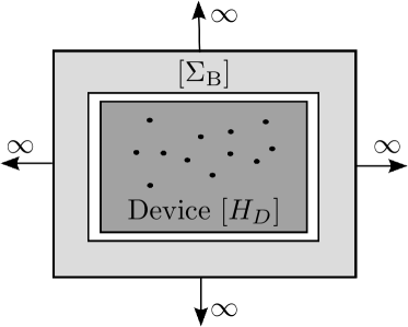
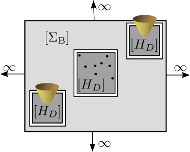
In this paper, we develop a Green’s function (GF) method which is able to efficiently treat large and finite sized ’patches’ embedded in an extended system, as shown in Fig. 1. The method combines an analytical formulation of the Green’s functions describing a pristine system Settnes et al. (2014a); Power and Ferreira (2011) with an adaptive recursive Green’s function method to described the patches. It allows for calculation of both local electronic and transport properties and for the inclusion of multiple leads and arbitrary geometries embedded within an extended sample.
This patched Green’s function method exploits an efficient calculation of the GF for an infinite pristine system using complex contour techniques. Using this GF, an open boundary self energy term can be included in the device Hamiltonian to describe its connection to an extended sample. The device region itself, containing nanostructures and/or leads, is then treated with an adaptive recursive method. We demonstrate the formulation using graphene, but it is generally applicable to all (quasi) 2D structures where the Green’s function for the infinite pristine system can be determined. Consequently, the patched Green’s function method is a versatile tool for efficient investigation of non-periodic nanostructures in extended two dimensional systems.
The rest of the paper is outlined as follows: the general formalism is developed in Section II.1 by calculating the open boundary self energy from the pristine GF. In Section II.2 we use graphene as an example to show the calculation of the pristine GF, while Section II.3 discusses the adaptive recursive method used to treat the device when including the boundary self energy. In Section III we use the developed method to study the local density of states of a graphene sample under the influence of a local strain field. As a result, we can compare local density of state (LDOS) maps with pseudomagnetic field distributions. In this way, we show the existence of Friedel-type oscillations along with pseudomagnetic field effects in the LDOS. Finally, in Section IV, we use the patched Green’s function technique to demonstrate the existence of vortex like current patterns in the presence of a perforation within an extended graphene sheet.
II Method
We consider the computational setup schematically shown in the left panel of Fig. 1, where a device region is embedded within an extended two dimensional system. This setup ensures that we are not including edge effects due to the finite-size of the simulation domain. Sajjad et al. (2013) The device region is described by a Hamiltonian, , which may include disorder, deformations, mean field terms or leads etc. This device region is embedded into an extended system by applying a self energy term, . To consider the setup in Fig. 1, we need two things: first, we need to construct to describe the extended part of the system and secondly, we need an efficient way to describe the device region while taking into account. Furthermore, the treatment of the device should be able to consider arbitrary geometries, including mutually disconnected patches within the extended system, as shown in the right panel of Fig. 1.
We describe the method in three steps:
-
A:
Derivation of the boundary self energy term, , in terms of the pristine lattice GFs.
-
B:
Calculation of the real-space GF needed in the self energy calculation. We use graphene as an example.
-
C:
Implementation of an adaptive RGF method to build the device region(s) efficiently while including the self energy term(s) .
II.1 Boundary self energy
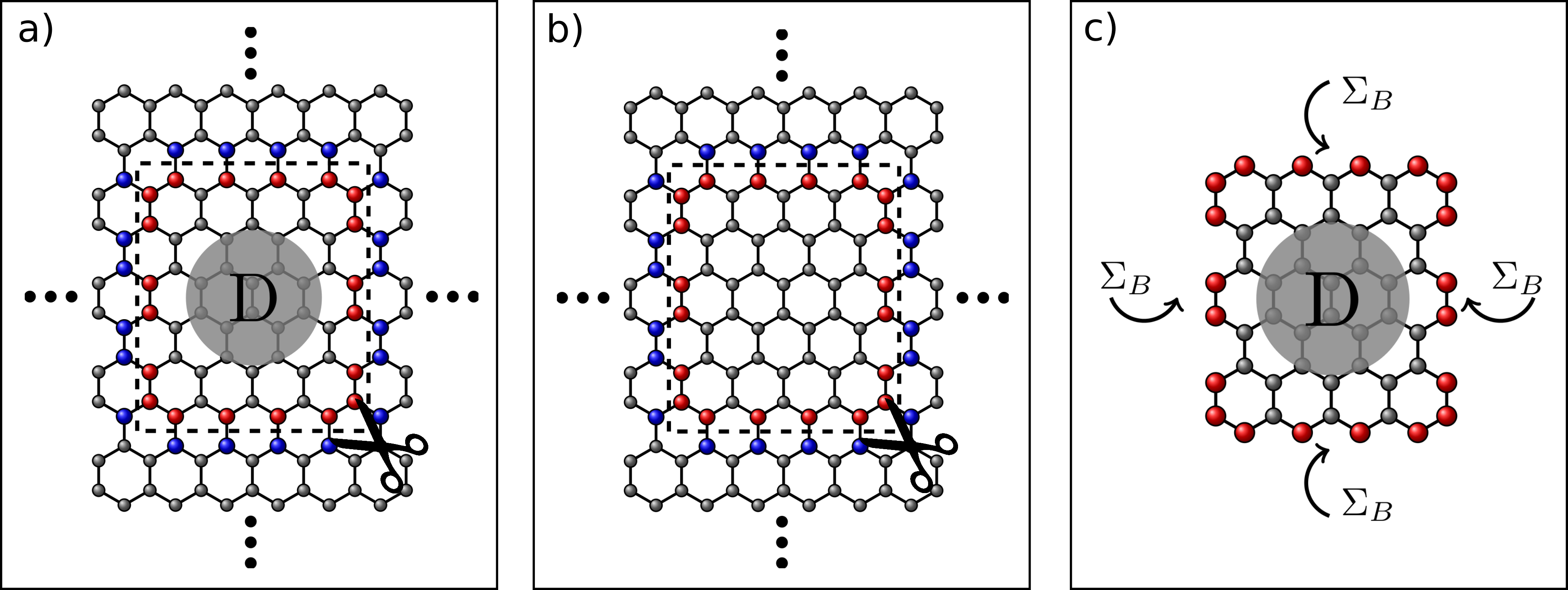
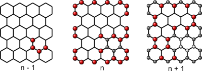
To construct the boundary self energy describing the extended region in Fig. 1, we consider the simple graphene example in Fig. 2a. Here a central device region, indicated by the dashed square, is embedded into an extended sheet. In this example both the extended area and the device region are assumed to be graphene-based, but the following arguments are general to any two dimensional material. We consider a division of the system into two parts: sites in the device (D) or sites in the extended sheet region. Furthermore, we subdivide the extended sheet into boundary sites (B) which are indicated by blue in Fig. 2 and have a non-zero Hamiltonian element coupling them to the device region, or ‘sheet’ sites which do not couple to the device region. Within a nearest-neighbour tight-binding Hamiltonian, the boundary sites in Fig. 2a are shown by blue symbols and have non-zero couplings to the device sites indicated by red symbols. We can now write the Hamiltonian for the entire system, in block matrix form, as
| (4) |
where the light shaded part of Eq. (4) represent an infinite Hamiltonian. The connections between device and sheet, (i.e. between the red and blue symbol sites) are contained in the off-diagonal blocks and .
We aim to replace the infinite Hamiltonian with a finite effective Hamiltonian, , which takes into account the extended sheet using a self energy term . To do this, we consider the connected system in panel a) of Fig. 2, and a disconnected system formed by removing the Hamiltonian elements and , corresponding to removing couplings crossing the dashed line in Fig. 2a. The GFs of the connected () and disconnected () systems can be related via the Dyson equation, and in particular we can write the GF of the connected device region as
| (5) |
Applying the Dyson equation again to obtain and inserting this into Eq. (5) allows us to simplify,
| (6) |
where the self energy term is given by
| (7) |
We note that the self energy in Eq. (7) is independent of the considered device and depends only on GF matrix elements connecting sites in the pristine surrounding ‘frame’ that remains when the device is removed from the full system. We take advantage of this to temporarily replace the device with a corresponding pristine region of the same size, as shown in panel b) of Fig. 2. The self-energy required to incorporate the finite pristine region into an infinite, pristine sheet is the same self energy, , that is required in Eq. (6). We can therefore write the required GF matrix, , in terms of the GF of the infinite pristine sheet, . These are related using the Dyson equation with a perturbation ,
| (8) |
The advantage of writing the self-energy in terms of the pristine sheet GFs, and , becomes clear in the next section, where we demonstrate an efficient method to calculate these two terms. It is worth noting that only needs to be calculated for the sites in D which connect to sites in B. These sites are indicated by red in Fig. 2 and are where the self-energy terms need to be added, as shown in panel c). In this way, the computations only involve matrices corresponding to the edge of the device and not the size of the full device region as straight forward inversion would require.
The calculation scheme can be summarized as follows:
-
1:
Calculate and using the methods outlined in Section II.2.
- 2:
- 3:
We note that this approach does not require a specific geometric shape of the device, nor does the device region need to be contiguous. We can treat different non-connected patches in an extended system, as shown in the right panel of Fig. 1, by extending the set D to include sites inside each patch and similarly expanding B to include sites at the boundary of each patch. The method presented in this section is applicable to any system where the connected, pristine GFs are easily obtainable as demonstrated in the next section using a tight-binding description of graphene as an example.
II.2 Real space graphene Green’s function
We now turn to the calculation of the real space GF of the pristine system, which is needed to calculate the self energy, , in Eq. (7) and Eq. (8). The approach required to calculate this quantity is demonstrated below for the case of a graphene sheet described with a nearest-neighbor tight-binding Hamiltonian, but is easily generalized for other cases.
This Hamiltonian is given by
| (9) |
where the sum runs over all nearest neighbour pairs and the carbon-carbon hopping integral is eV. The graphene hexagonal lattice can be split into two triangular sublattices, which we denote A and B, and neighbouring sites reside on opposite sublattices to each other. Using Bloch functions, the Hamiltonian can be rewritten in reciprocal space as Castro Neto et al. (2009)
| (10) |
where the matrix form arises from sublattice indexing within a 2 atom unit cell and we have used the definition , with the lattice vectors and and the carbon-carbon distance. With this definition of the unit vectors we have the armchair direction along the y-axis (and zigzag along the x-axis).
The eigenenergies and eigenstates of the system are easily obtained from this form of the Hamiltonian, and transforming back to real space allows us to write the desired Green’s function between sites and as Bena (2009); Power and Ferreira (2011)
| (11) |
where is the energy, is the area of the first Brillouin zone. The position of the unit cell containing site is denoted by with and being integers. Finally we use the definition , when and are on the same sublattice and if is on the A sublattice and is on the B sublattice and when is on B and on A.
To simplify the notation we introduce the dimensionless k-vectors and such that , and write the separation vector in terms of the lattice vectors . Inserting this into Eq. (11) gives
| (12) |
Eq. (12) can be solved using a two-dimensional numerical integration, but as we require Eq. (12) for each Green’s function element individually, we wish to increase the performance by doing one integration analytically using complex contour techniques.
Following the approach of Ref. Power and Ferreira, 2011, we use as complex variable and consider the poles, , of the denominator
| (13) |
The sign of the pole must be selected carefully to ensure that it lies within the integration contour, i.e. , for contours in the positive half plane corresponding to the situation . Care must also be taken with the additional phase terms that arise for opposite sublattice GFs.
Using the residue theorem and integrating over a rectangular Brillouin zone, and , we finally reduce Eq. (12) to
| (14) |
with given by Eq. (13). A similar expression to Eq. (14) can be derived when using as first integration variable. Power and Ferreira (2011) The above derivation is based upon a nearest neighbour model, but can be generalised to also include, for example, second nearest neighbour terms Lawlor and Ferreira (2014) or uniaxial strains. Power et al. (2012)
We can now use Eq. (14) to calculate the elements of the required GFs, and , defined in Section II.1. In this way, Eq. (14) can be used to fill up the elements of the desired matrices one at a time. Since we need GF matrices of size and , where and are the number of sites at the edge of the device region and in the region B, respectively, it could seem very ineffective to calculate one element at a time. However, the total number of GF elements to be calculated is greatly reduced by the symmetries of the pristine graphene lattice. The lattice itself is six-fold symmetric and each of these six identical wedges is in turn mirror symmetric, resulting in a -fold degeneracy of the GFs indexed by site separation vectors. Additionally, many of the required elements in and are identical. For instance, the onsite and nearest neighbour GF element appear many times, but only need to be calculated once. Taking the device region in Fig. 2 as example we have , yielding 400 individual elements for a brute force calculation. Instead, using symmetries and duplicates, we only need to calculate 38 and 42 elements when determining and , respectively. The reduction becomes more significant for larger systems, as we generally only need to add the GF elements corresponding to the longest couplings. Consequently, only a small percentage of the GF elements need to be calculated individually and their values for frequently used separations and energies can be stored or reused to enable extremely fast calculation of the required self energies.
II.3 Adaptive recursion for device region
In this section we consider the device region where the boundary self energy can be added at the edge. The full GF of the device region is given by , where we have simplified the notation from Eq. (6). From this GF both transport and local properties can be obtained. However, for most purposes we do not require every element of the Green’s function matrix element in the device region, and so to avoid a time consuming full matrix inversion, recursive methods are often applied Areshkin and Nikolić (2010); Lewenkopf and Mucciolo (2013); Yang et al. (2011); Thorgilsson et al. (2014); Metalidis and Bruno (2005); Cresti et al. (2003); Sajjad et al. (2013); Costa Girão and Meunier (2013).
This section outlines an adaptive recursion method which efficiently includes the boundary self energy as well as an arbitrary device region shape and configuration (and number) of leads. Alternative approaches have been developed to treat arbitrary shaped regions with multiple leads Kazymyrenko and Waintal (2008); Wimmer and Richter (2009); Costa Girão and Meunier (2013). These so-called knitting-algorithms add single sites at a time. They rely on a complicated categorizing of sites into different intermediate updating blocks making the theory and implementation cumbersome. Hence, we use an approach similar to the ones in Refs. Areshkin and Nikolić, 2010; Yang et al., 2011; Thorgilsson et al., 2014, and employ an adaptive partitioning of the Hamiltonian matrix in order to bring it into the desired tridiagonal form suitable for recursive methods.
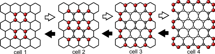
Calculating physical properties generally requires certain GFs connecting a specific set of sites in the device region. These sites of interest, for example, could be sites where we want to introduce defects, or couple to probes for transport calculations, or measure properties like the local density of states. We focus first on the general partitioning process, and then demonstrate how it can be quickly modified to account for the edge self-energy terms. We begin by placing all these sites of interest into recursive cell 1, as shown by the red sites in Fig. 3. We emphasize that the cells in this process are not of a fixed size and may consist of arbitrary sites which are not necessarily connected. Cell 2 is determined by selecting all the remaining unpartitioned sites which couple directly to sites in cell 1 via a non-zero Hamiltonian matrix element. In the example in Fig. 3, this consists of nearest neighbor sites of those in cell 1, which are not themselves in cell 1. This process is repeated until all sites in the device region have been allocated a cell, and is demonstrated schematically in the panels of Fig. 3 where red sites indicate the current cell, and dark gray or white sites indicate sites added to the previous cell, or to earlier cells, respectively.
With the resultant block tridiagonal Hamiltonian, we can now employ the usual recursive algorithm, starting from cell , so that the final step yields the required GF sites in cell . These terms can then be used to calculate observable quantities like transmission, LDOS, etc. Afterwards a reverse recursive sweep from to can be implemented to efficiently map local quantities like bond currents or LDOS everywhere within the device regionLewenkopf and Mucciolo (2013). For completeness the full recursive method is summarized in Appendix A including the reverse sweep. We emphasize that the presented method is not unique to graphene systems, but can be employed to arbitrary tight-binding-like models.
Including the boundary self-energy
We now return to the specific case at hand where the recursive method outlined above needs to be adapted carefully to take account of the boundary self energy. In general is a non-hermitian dense matrix connecting all edge sites of the device region. Therefore it is essential to assign all edge sites to the same cell. This principle is shown in Fig. 4. If cell contains sites which connect to an edge site, then cell must contain not only the edge sites directly connecting to cell , but also all other edge sites, as these are connected to each other via . In this way, the cell, , must then contain all the sites connecting to cell , i.e. also connecting to the edge, but not included in cell . The full cell partitioning algorithm, including this step, is given in Appendix A.
III Inhomogeneous strain fields in graphene bubbles
In this section, we employ the patched Green’s function method to a locally strained graphene system, demonstrating how it can prove a useful tool in investigating local properties of non-periodic nanostructures in extended two dimensional systems.
Strain engineering has been proposed as a method to manipulate the electronic, optical and magnetic properties of graphene. Low et al. (2011); Guinea et al. (2009); Jones and Pereira (2014); Qi et al. (2014); Neek-Amal and Peeters (2012a); Lu et al. (2012); Carrillo-Bastos et al. (2014); Juan et al. (2011); Neek-Amal et al. (2013); Neek-Amal and Peeters (2012b); Pereira et al. (2009, 2009); Pereira and Castro Neto (2009); Power et al. (2012); Pereira et al. (2010); Moldovan et al. (2013) It is based on the close relation between the structural and electronic properties of graphene. The application of strain can lead to effects like bandgap formation Pellegrino et al. (2010), transport gaps Low et al. (2011) and pseudomagnetic fields (PMFs). Guinea et al. (2009); Qi et al. (2014); Jones and Pereira (2014)
Uniaxial or isotropic strain will not produce PMFs, although it has been shown to shift the Dirac cone of graphene and induce additional features in the Raman signal. Ni et al. (2008) On the other hand, inhomogeneous strain fields can introduce PMFs. In this case, the altered tight binding hoppings mimic the role of a gauge field in the low energy effective Dirac model of graphene. Suzuura and Ando (2002); Vozmediano et al. (2010) For example Guinea et al. Guinea et al. (2009) demonstrated that nearly homogeneous PMFs can be generated by applying triaxial strain. One of the most striking consequences of homogeneous PMFs is the appearance of a Landau-like quantization. Guinea et al. (2009); Neek-Amal et al. (2013) Scanning tunnelling spectroscopy on bubble-like deformations see this quantization, where the observed pseudo-Landau levels corresponds to PMFs stronger than 300 T. Lu et al. (2012); Levy et al. (2010)
Deformations can be induced in graphene samples by different techniques like pressurizing suspended graphene Bunch et al. (2008); Qi et al. (2014) or by exploiting the thermal expansion coefficients of different substrates.Lu et al. (2012) As a result, introducing nonuniform strain distributions at the nanoscale is a promising way of realizing strain engineering. The standard theoretical approach to treat strain effects employs continuum mechanics to obtain the strain field. Several studies improve the accuracy by replacing the continuum mechanics by classical molecular dynamics simulations. Neek-Amal and Peeters (2012a); Qi et al. (2014, 2013) The strain field can then be coupled to an effective Dirac model of graphene to study the generation of PMFs in various geometries. In most studies, only the PMF distribution is considered as opposed to experimentally observable quantities like local density of states. The framework presented in Section II enables us to treat the effect of strain on the LDOS directly from a tight-binding Hamiltonian. Consequently, we are now able to describe a single bubble in an extended system without applying periodic boundary conditions which may introduce interactions between neighboring bubbles. The dual recursive sweep then allows for efficient calculation of local properties everywhere in the device region surrounding a bubble, enabling us to investigate spatial variations in real space LDOS maps. In this section we only treat one nanostructure, but the patched Green’s function technique efficiently handles several spatially separated nanostructures, as the separation is added very efficiently through the self energy term.
To account for strain within a tight binding approach we modify the hopping parameters.Pereira et al. (2009); Moldovan et al. (2013); Carrillo-Bastos et al. (2014) The nearest neighbour hopping in Eq. (9) between site and is given by the new distance, , between the sites,
| (15) |
where the coefficient . Pereira et al. (2009) We treat the deformation problem by applying an analytical displacement profile matched against experimental data for pressurized suspended graphene. Yue et al. (2012) Here and are the in-plane and vertical displacements, respectively, which are induced by the applied strain. For a rotationally symmetric aperture with radius , these are given, in spherical coordinates , as
| (16a) | ||||
| (16b) | ||||
for . Here is the maximal height of the bubble and is a constant relating the out-of-plane and in-plane deformations. Yue et al. (2012) We note that this profile gives rise to a sharp edge at , and many of the features we discuss below emerge from the strongly clamped nature of this bubble type.
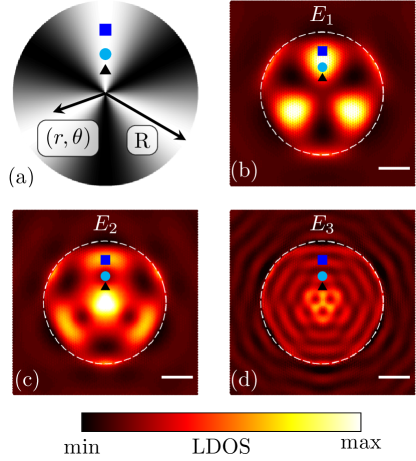
As shown in Appendix B, rotationally symmetric strain profiles give rise to threefold symmetric PMFs in the effective Dirac model. This is shown in Fig. 5a for the strain profile considered in Eq. (16). As discussed in earlier studies, Moldovan et al. (2013); Carrillo-Bastos et al. (2014) we get an asymmetric sublattice occupancy such that the LDOS of each sublattice has a threefold symmetric distribution following the PMF while rotated compared to the opposite sublattice. In all calculations below, we therefore show only one sublattice, as the result for the opposite sublattice can be obtained by a rotation and the total pattern is a superposition of both. Jones and Pereira (2014); Juan et al. (2011)
Comparing the PMF distribution in Fig. 5a with the calculated LDOS maps at different energies in Fig. 5b-d for a bubble of radius nm and height nm, we immediately notice that the threefold symmetry is also present in the LDOS maps. However, the spatial LDOS maps have significant additional details compared to the PMF distribution.
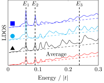
In Fig. 6 we calculate the energy dependent LDOS at the positions indicated by symbols (square, circle and triangle) in Fig. 5. We first consider the average of the LDOS within the ‘slice’ containing the symbols, shown by the bottom (red) curve in Fig. 6. Two distinct oscillation types are observed, and we argue that these can be divided into Friedel-type and PMF-induced features. At high energies in particular we notice regularly space oscillations with an approximate period of . These are consistent with Friedel-type oscillations related to the size of the structure and emerging from interferences between electrons scattered at opposite sides of the bubble. An exact treatment needs to take into account the renormalized Fermi velocity, , due to the average change in bond length. Pellegrino et al. (2011) At lower energies we observe distinct peaks which are not equally spaced (the first two appear at and ). We will show that these are due to pseudomagnetic effects and we refer to them as pseudo Landau levels.
Besides the Friedel oscillation associated with the bubble radius, we also have similar oscillations associated with the distances to different edges of the bubble. These features are highly position dependent, and explain the differences between the three single position curves in Fig. 6. When considering the average, these position dependent oscillations are washed out (bottom curve in Fig. 6), leaving only the oscillation dependent on the structure size. However, at individual positions these oscillations can have a considerable impact. Returning to the individual position STS curves in Fig. 6, we note that the peak at is only dominant for the points indicated by the square and triangle. It is suppressed by Friedel-type interferences at the circle point, which is also clear from the LDOS map in Fig. 5c.
The amplitude of the Friedel-type oscillations is determined by the strength of scattering near the bubble edges. The clamped edge implied by the strength profile in Eq. (16) gives rise to significant strain fields along this edge, leading to a sharp, strong perturbation. More realistic profiles calculated from molecular dynamics also indicate strong perturbations near the edges of clamped bubbles.Qi et al. (2014) Our results indicate that edge scattering effects may significantly affect LDOS behavior in clamped bubble systems and even mask PMF-induced features.
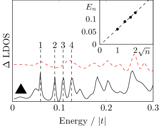
To treat the oscillations due to the feature size and edge sharpness in more detail, we calculate the LDOS for an artificial system only taking into account the strain field along a small ring around the edge, see Fig. 7 (dashed red line). In this way, only Friedel-type features are expected within the structure. If we compare to the full calculation (full black line in Fig. 7), we notice that the oscillations at higher energies are present in both calculations, whereas the sharp peaks are only present in the full calculation. This confirms the Friedel nature of the higher energy oscillations and suggests the lower energy peaks are due to an alternative mechanism. To confirm that the sharp peaks are due to pseudomagnetic effects, we compare the peak positions to the standard form expected for Landau levels in graphene , where is the electron charge, is the magnetic field and is the peak number. Castro Neto et al. (2009) The peaks labelled 1-4 in Fig. 7 display the dependence characteristic of Landau levels in graphene, as shown in the inset of Fig. 7. The size of the PMF can furthermore be inferred to be T from the inset.
To conclude, we discussed how the features in the LDOS spectra of clamped graphene bubbles can be explained by a combination of size-dependent scattering and PMF-induced effects like pseudo Landau quantization. Significant strain fields near the edge of the structure give rise to strong Friedel-type oscillations in the LDOS and these oscillations envelope the effect of a PMF. We must therefore be careful to distinguish between the two type of oscillations when investigating the electronic effects of PMFs induced by inhomogeneous strain fields.
IV Vortex currents near perforations
In this section we investigate local transport properties near antidots (i.e. perforations) in a graphene sheet. Periodic arrays of antidots have been studied as a way to open a bandgap in graphene Pedersen et al. (2008); Gunst et al. (2011); Fürst et al. (2009) or to obtain waveguiding effects. Pedersen et al. (2012); Power and Jauho (2014) Furthermore, a single perforation in a graphene sheet has been considered as a nanopore for DNA sensing. Schneider et al. (2010); Merchant et al. (2010)
Several studies show that the electronic structure of antidots is closely related to the exact edge geometry. Power and Jauho (2014); Pedersen et al. (2008); Settnes et al. (2014b) Experimental fabrication techniques like block copolymer Kim et al. (2010); Bai et al. (2010); Kim et al. (2012) or electron beam lithography, Eroms and Weiss (2009); Xu et al. (2013); Oberhuber et al. (2013) inevitably lead to disorder and imperfect edges. However, it may be possible to control the edge geometry of the antidot by heat treatment Jia et al. (2009); Xu et al. (2013), or selective etching. Oberhuber et al. (2013); Pizzocchero et al. (2014)
Motivated by the interest in how current flows in antidot systems, we apply the patched GF method to a single perforation in a graphene sheet. The method allows us to study the perforation with no influence from periodic repetition or finite sample size. Additionally, the combination of recursive methods and a boundary self-energy allows for investigation of antidot sizes realizable experimentally. Cagliani et al. (2014); Bai et al. (2010); Merchant et al. (2010) In fact we consider both an example antidot with perfect edges and an exact structure found from high resolution transmission electron microscope (TEM) images using pattern recognition. Kling et al. (2014); Vestergaard et al. (2014)
To investigate current on the nanoscale, recent experiments have realized multiple STM-systems. Baringhaus et al. (2014); Sutter et al. (2008); Clark et al. (2014); Li et al. (2013) These allow for individual manipulation of several STM-tips in order to make electrical contact to the sample near the considered nanostructure. Theoretically, we previously considered multiple STM setups allowing for both fixed and scanning probes. Settnes et al. (2014a, b) The method presented here allows for not only transmission calculations but also calculation of local electronic and transport properties in the presence of multiple point probes. At the same time large separations between the different probes and/or nanostructures are easily included as additional separation is achieved in a very computationally efficient manner through the self energy term connecting multiple patches. The combination of large spatial separation between features, while still enabling calculation of local electronic and transport properties, can prove a useful tool in investigating extended two dimensional systems where we take special interest in a particular region of the extended sample.
In order to consider transmissions and current patterns, we add leads to the system through inclusion of a lead self-energy term, , where is the coupling element between the device site and the lead. To model the structureless lead, we use the surface GF of a single atomic chain, as this has a constant DOS in the considered energy range. The distance dependence in is necessary to avoid an unphysical coupling between different lattice sites via the lead. We therefore add a -dependence for the off-diagonal terms 111The surface Green’s function of the single atomic chain is given by . Economou (2005) We chose as this gives a constant DOS within the considered energies. The distance dependence for off-diagonal finally gives the GF, where , as appropriate for a structureless three-dimensional free electron gas. Economou (2005)
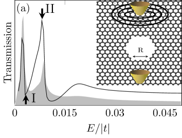
First, we consider a zigzag-edged antidot with side length nm, where is the length of the graphene unit cell and Å. This is comparable to experimental sizes where sub-20-nm feature sizes have been reported. Merchant et al. (2010); Kim et al. (2010); Bai et al. (2010); Kim et al. (2012) The antidot is between two probes placed nm apart, as shown schematically in the inset of Fig. 8a. The main panel of Fig. 8a shows the transmission as a function of energy for this dual point probe setup. We note the distinct transmission peaks. As explained in Ref. Settnes et al., 2014b, these peaks are related to localized states along the zigzag edges. As a consequence, we notice the correspondence between the peaks in the transmission and the peaks in the LDOS around the edge, see shaded area in Fig. 8a.
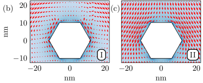
Next, we calculate the bond currents from the top lead. The bond current between site and from lead are calculated, as explained in Appendix A, by , where is the Hamiltonian matrix element connecting site and . The bond currents around the zigzag antidot for the energies indicated in Fig. 8a are shown in Figs. 8b and 8c. In this way, we see that the transmission dips are related to vortex like current paths. These vortex paths create a larger ‘effective size’ for the antidot at this energy, characterized by a region around the antidot avoided by the current paths. On the other hand, at the transmission peaks the current passes near to the antidot edge.
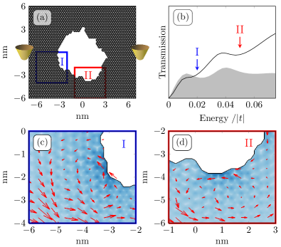
The antidot considered in Fig. 8, although of realistic size, is an idealization, as experimental perforations will inevitably contain imperfections. To consider a more realistic case, we turn to a perforation observed in experimental TEM images. Using pattern recognition Kling et al. (2014); Vestergaard et al. (2014) the positions of the individual carbon atoms are obtained from high resolution TEM images (see Fig. 9 of Ref. Vestergaard et al., 2014). Pristine graphene is added around the experimentally obtained perforation to obtain the system shown in Fig. 9a. From the transmission (see Fig. 9b), we notice that peaks are still present, but broadened by the disorder. Considering the two energies I and II in Fig. 9b and comparing their spatial current maps, we find that certain positions around the antidot are responsible for the additional backscattering causing the transmission dips. Dip I corresponds to a vortex pattern at the left side of the antidot (see Fig. 9c), whereas the dip at II is caused by a vortex pattern at the bottom of the antidot (see Fig. 9d). This result suggests that electrons at different energies see a different effective perforation size and shape and are scattered accordingly.
V Conclusion
We have expanded the standard recursive Green’s function method to calculate local and transport properties enabling calculations in extended non-periodic systems. We exploit an efficient calculation of the pristine two-dimensional GF using complex contour methods. Once calculated, the pristine GFs are used to determine a boundary self energy term describing the extended system. In this way, we can treat a finite device region embedded within an extended sample.
We first demonstrated how this approach is able to efficiently treat the electronic properties of strained bubbles in an extended graphene sheet. Considering a clamped bubble, we have shown that the finite size gives rise to Friedel-type oscillations in the density of states. This effect mixes with any pseudomagnetic effects arising from the strain field. We show that the edge effects can cloud pseudomagnetic signatures in the LDOS by adding additional structure which is not directly related to pseudomagnetic effects.
Secondly, we showed how finite leads can be added to a patched device region to efficiently calculate transport properties for spatially separated features, while still being able to map local properties in various parts of the system. In particular, we investigated the current flow around perforations of a graphene lattice. Both idealized geometries and experimental geometries obtained from high resolution TEM images were considered. The transmissions show distinct dips caused by localized states along zigzag segments of the perforations. The transmission dips were associated with vortex-like current paths formed near the perforation edges.
We have demonstrated the versatility of this novel approach to the popular recursive GF method. The method allows for calculation of the same local and transport properties as standard methods, but adds the ability to treat large non-periodic structures embedded in extended samples. We can extend the present method beyond nearest neighbor and to relevant alloys like hBN or transition metal dichalcogenides. We therefore predict that the patched Green’s function method will prove a valuable tool in the investigation of nanostructures in two dimensional materials.
Acknowledgements We thank B.K. Nikolic for enlightening discussions of recursive methods applied to arbitrary geometries. We also thank J. Kling for providing the experimental TEM data used in modelling current paths around realistic perforations. The work was supported by the Villum Foundation, Project No. VKR023117. The Center for Nanostructured Graphene (CNG) is sponsored by the Danish Research Foundation, Project DNRF58.
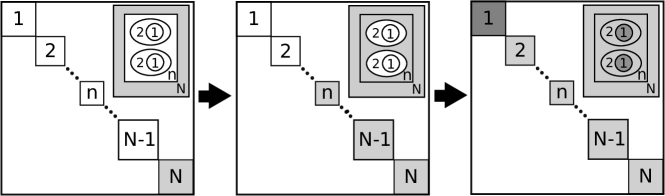

Appendix A Recursive Algorithm
To obtain a tridiagonal Hamiltonian we let cell contain all sites of interest. Then following the algorithm outlined below we assign all sites into cells.
-
1:
Let denote all sites in cell and denote all sites not yet assigned to a cell.
-
2:
Find all sites for which where and . Denote these sites .
-
2a:
If contains an edge site, then all remaining edge sites are added to .
-
3:
Sites in are removed from
-
4:
Repeat 1-3 until all sites are assigned to a cell.
Step 2a is included if we require an edge self energy term as described in Section II.
Assuming the block tridiagonal partitioning obtained from the algorithm above, we make an update sweep starting from cell , as shown schematically in Fig. 10. The steps are calculated using the recursive relations Lewenkopf and Mucciolo (2013)
| (17a) | ||||
| (17b) | ||||
| (17c) | ||||
where one of the terms includes the self energy and terms are included if we calculate transmission. After the sweep is complete, the fully connected GF of cell is obtained as . As all sites of interest are placed in this cell, we can now calculate observables involving these sites. For example we calculate transmission, , between lead L and L’ using these GFs.
| (18) |
where and () is the retarded (advanced) GF connecting the two leads L and L’.
In order to obtain other blocks of the full GF matrix, we need to store the GF matrix, , for each cell as we sweep from to . The stored blocks are shown in light gray on Fig. 10.
To obtain the LDOS at site , , we need the diagonal of the GF matrix. We calculate the block diagonal from a reversed sweep from to , see Fig. 10. The reversed sweep uses the block diagonals, , from the first sweep to calculate the full diagonal GF, ,
| (19) |
Finally, we want to obtain bond currents for the state leaving a lead . This can be calculated by . Remembering that the leads are assigned to cell , we need the off-diagonal blocks, and , in order to obtain bond currents. Using the stored GFs from the first sweep we can calculate the needed off-diagonals,
| (20a) | ||||
| (20b) | ||||
Appendix B Pseudomagnetic field for rotational symmetric strain field
The strain tensor is generally given as
| (21) |
where is the in-plane deformation field and is the out-of-plane deformation.Vozmediano et al. (2010)
A general two dimensional strain field, , leads to a gauge field in the effective Dirac Hamiltonian of graphene Suzuura and Ando (2002); Vozmediano et al. (2010)
| (22) |
which in turn gives a PMF
| (23) |
Eqs. (22) and (23) imply that the x-axis is chosen along the zigzag direction of the graphene lattice.
Now restricting ourselves to rotationally symmetric deformations, and , while using polar coordinates yields
| (24) |
with . We notice from Eq. (24) that the PMF for a rotationally symmetric displacement field is always 6-fold symmetric. On the other hand, the magnitude depends on both the in-plane and out-of-plane displacement.
Considering the displacement field in Eq. (16) we now obtain a PMF of the form,
| (25) |
Taking into account the scaling , we obtain a final scaling of the PMF with the size of the bubble, .
References
- Geim and Grigorieva (2013) A. K. Geim and I. V. Grigorieva, Nature 499, 419 (2013).
- Fiori et al. (2014) G. Fiori, F. Bonaccorso, G. Iannaccone, T. Palacios, D. Neumaier, A. Seabaugh, S. K. Banerjee, and L. Colombo, Nature Nanotechnology 9, 768 (2014).
- Bai et al. (2010) J. Bai, X. Zhong, S. Jiang, Y. Huang, and X. Duan, Nature nanotechnology 5, 190 (2010).
- Schedin et al. (2007) F. Schedin, A. K. Geim, S. V. Morozov, E. W. Hill, P. Blake, M. I. Katsnelson, and K. S. Novoselov, Nature Materials 6, 652 (2007).
- Qi et al. (2013) Z. Qi, D. A. Bahamon, V. M. Pereira, H. S. Park, D. K. Campbell, and A. H. C. Neto, Nano letters 13, 2692 (2013).
- Novoselov and Castro Neto (2012) K. S. Novoselov and A. H. Castro Neto, Physica Scripta T146, 014006 (2012).
- Castro Neto et al. (2009) A. H. Castro Neto, N. M. R. Peres, K. S. Novoselov, and A. K. Geim, Reviews of Modern Physics 81, 109 (2009).
- Lewenkopf and Mucciolo (2013) C. Lewenkopf and E. Mucciolo, Journal of Computational Electronics 12, 203 (2013).
- Datta (1997) S. Datta, Electronic Transport in Mesoscopic Systems (Cambridge University Press, 1997).
- Foa Torres et al. (2014) L. E. F. Foa Torres, S. Roche, and J.-C. Charlier, Introduction to Graphene-Based Nanomaterials (Cambridge University Press, 2014).
- Kazymyrenko and Waintal (2008) K. Kazymyrenko and X. Waintal, Physical Review B 77, 115119 (2008).
- Wimmer and Richter (2009) M. Wimmer and K. Richter, Journal of Computational Physics 228, 8548 (2009).
- Baringhaus et al. (2014) J. Baringhaus, M. Ruan, F. Edler, A. Tejeda, M. Sicot, A.-P. Li, Z. Jiang, E. H. Conrad, C. Berger, C. Tegenkamp, and W. A. de Heer, Nature 506, 349 (2014).
- Sutter et al. (2008) P. W. Sutter, J.-I. Flege, and E. A. Sutter, Nature Materials 7, 406 (2008).
- Settnes et al. (2014a) M. Settnes, S. R. Power, D. H. Petersen, and A.-P. Jauho, Phys. Rev. Lett. 112, 096801 (2014a).
- Power and Ferreira (2011) S. R. Power and M. S. Ferreira, Physical Review B 83, 155432 (2011).
- Sajjad et al. (2013) R. N. Sajjad, C. A. Polanco, and A. W. Ghosh, Journal of Computational Electronics 12, 232 (2013).
- Bena (2009) C. Bena, Physical Review B 79, 125427 (2009).
- Lawlor and Ferreira (2014) J. A. Lawlor and M. S. Ferreira, ArXiv e-prints (2014), arXiv:1411.6240 .
- Power et al. (2012) S. R. Power, P. D. Gorman, J. M. Duffy, and M. S. Ferreira, Phys. Rev. B 86, 195423 (2012).
- Areshkin and Nikolić (2010) D. A. Areshkin and B. K. Nikolić, Physical Review B 81, 155450 (2010).
- Yang et al. (2011) M. Yang, X.-J. Ran, Y. Cui, and R.-Q. Wang, Chinese Physics B 20, 097201 (2011).
- Thorgilsson et al. (2014) G. Thorgilsson, G. Viktorsson, and S. Erlingsson, Journal of Computational Physics 261, 256 (2014).
- Metalidis and Bruno (2005) G. Metalidis and P. Bruno, Physical Review B 72, 235304 (2005).
- Cresti et al. (2003) A. Cresti, R. Farchioni, G. Grosso, and G. P. Parravicini, Physical Review B 68, 075306 (2003).
- Costa Girão and Meunier (2013) E. Costa Girão and V. Meunier, Journal of Computational Electronics 12, 123 (2013).
- Low et al. (2011) T. Low, F. Guinea, and M. I. Katsnelson, Physical Review B 83, 195436 (2011).
- Guinea et al. (2009) F. Guinea, M. I. Katsnelson, and A. K. Geim, Nature Physics 6, 30 (2009).
- Jones and Pereira (2014) G. W. Jones and V. M. Pereira, New Journal of Physics 16, 093044 (2014).
- Qi et al. (2014) Z. Qi, A. L. Kitt, H. S. Park, V. M. Pereira, D. K. Campbell, and A. H. Castro Neto, Phys. Rev. B 90, 125419 (2014).
- Neek-Amal and Peeters (2012a) M. Neek-Amal and F. M. Peeters, Phys. Rev. B 85, 195445 (2012a).
- Lu et al. (2012) J. Lu, A. H. Castro Neto, and K. P. Loh, Nature communications 3, 823 (2012).
- Carrillo-Bastos et al. (2014) R. Carrillo-Bastos, D. Faria, A. Latgé, F. Mireles, and N. Sandler, Physical Review B 90, 041411 (2014).
- Juan et al. (2011) F. D. Juan, A. Cortijo, M. A. H. Vozmediano, and A. Cano, Nature Physics 7, 810 (2011).
- Neek-Amal et al. (2013) M. Neek-Amal, L. Covaci, K. Shakouri, and F. M. Peeters, Physical Review B 88, 115428 (2013).
- Neek-Amal and Peeters (2012b) M. Neek-Amal and F. M. Peeters, Physical Review B 85, 195446 (2012b).
- Pereira et al. (2009) V. M. Pereira, A. H. Castro Neto, and N. M. R. Peres, Physical Review B 80, 045401 (2009).
- Pereira and Castro Neto (2009) V. M. Pereira and A. H. Castro Neto, Phys. Rev. Lett. 103, 046801 (2009).
- Pereira et al. (2010) V. M. Pereira, R. M. Ribeiro, N. M. R. Peres, and A. H. Castro Neto, EPL (Europhysics Letters) 92, 67001 (2010).
- Moldovan et al. (2013) D. Moldovan, M. Ramezani Masir, and F. M. Peeters, Physical Review B 88, 035446 (2013).
- Pellegrino et al. (2010) F. M. D. Pellegrino, G. G. N. Angilella, and R. Pucci, Physical Review B 81, 035411 (2010).
- Ni et al. (2008) Z. H. Ni, T. Yu, Y. H. Lu, Y. Y. Wang, Y. P. Feng, and Z. X. Shen, ACS Nano 2, 2301 (2008).
- Suzuura and Ando (2002) H. Suzuura and T. Ando, Phys. Rev. B 65, 235412 (2002).
- Vozmediano et al. (2010) M. Vozmediano, M. Katsnelson, and F. Guinea, Physics Reports 496, 109 (2010).
- Levy et al. (2010) N. Levy, S. A. Burke, K. L. Meaker, M. Panlasigui, A. Zettl, F. Guinea, A. H. Castro Neto, and M. F. Crommie, Science 329, 544 (2010).
- Bunch et al. (2008) J. S. Bunch, S. S. Verbridge, J. S. Alden, A. M. van der Zande, J. M. Parpia, H. G. Craighead, and P. L. McEuen, Nano Letters 8, 2458 (2008).
- Yue et al. (2012) K. Yue, W. Gao, R. Huang, and K. M. Liechti, Journal of Applied Physics 112, 083512 (2012).
- Pellegrino et al. (2011) F. M. D. Pellegrino, G. G. N. Angilella, and R. Pucci, Phys. Rev. B 84, 195404 (2011).
- Pedersen et al. (2008) T. G. Pedersen, C. Flindt, J. G. Pedersen, N. A. Mortensen, A.-P. Jauho, and K. Pedersen, Physical Review Letters 100, 136804 (2008).
- Gunst et al. (2011) T. Gunst, T. Markussen, A.-P. Jauho, and M. Brandbyge, Phys. Rev. B 84, 155449 (2011).
- Fürst et al. (2009) J. A. Fürst, J. G. Pedersen, C. Flindt, N. A. Mortensen, M. Brandbyge, T. G. Pedersen, and A. P. Jauho, New Journal of Physics 11, 095020 (2009).
- Pedersen et al. (2012) J. G. Pedersen, T. Gunst, T. Markussen, and T. G. Pedersen, Phys. Rev. B 86, 245410 (2012).
- Power and Jauho (2014) S. R. Power and A.-P. Jauho, Phys. Rev. B 90, 115408 (2014).
- Schneider et al. (2010) G. F. Schneider, S. W. Kowalczyk, V. E. Calado, G. Pandraud, H. W. Zandbergen, L. M. K. Vandersypen, and C. Dekker, Nano letters 10, 3163 (2010).
- Merchant et al. (2010) C. A. Merchant, K. Healy, M. Wanunu, V. Ray, N. Peterman, J. Bartel, M. D. Fischbein, K. Venta, Z. Luo, A. T. C. Johnson, and M. Drndić, Nano letters 10, 2915 (2010).
- Settnes et al. (2014b) M. Settnes, S. R. Power, D. H. Petersen, and A.-P. Jauho, Phys. Rev. B 90, 035440 (2014b).
- Kim et al. (2010) M. Kim, N. S. Safron, E. Han, M. S. Arnold, and P. Gopalan, Nano letters 10, 1125 (2010).
- Kim et al. (2012) M. Kim, N. S. Safron, E. Han, M. S. Arnold, and P. Gopalan, ACS Nano 6, 9846 (2012).
- Eroms and Weiss (2009) J. Eroms and D. Weiss, New Journal of Physics 11, 095021 (2009).
- Xu et al. (2013) Q. Xu, M.-Y. Wu, G. F. Schneider, L. Houben, S. K. Malladi, C. Dekker, E. Yucelen, R. E. Dunin-Borkowski, and H. W. Zandbergen, ACS Nano 7, 1566 (2013).
- Oberhuber et al. (2013) F. Oberhuber, S. Blien, S. Heydrich, F. Yaghobian, T. Korn, C. Schüller, C. Strunk, D. Weiss, and J. Eroms, Applied Physics Letters 103, 143111 (2013).
- Jia et al. (2009) X. Jia, M. Hofmann, V. Meunier, B. G. Sumpter, J. Campos-Delgado, J. M. Romo-Herrera, H. Son, Y.-P. Hsieh, A. Reina, J. Kong, M. Terrones, and M. S. Dresselhaus, Science 323, 1701 (2009).
- Pizzocchero et al. (2014) F. Pizzocchero, M. Vanin, J. Kling, T. W. Hansen, K. W. Jacobsen, P. Bøggild, and T. J. Booth, The Journal of Physical Chemistry C 118, 4296 (2014).
- Cagliani et al. (2014) A. Cagliani, D. Mackenzie, L. Tschammer, F. Pizzocchero, K. Almdal, and P. Bøggild, Nano Research 7, 743 (2014).
- Kling et al. (2014) J. Kling, J. S. Vestergaard, A. B. Dahl, N. Stenger, T. J. Booth, P. Bøggild, R. Larsen, J. B. Wagner, and T. W. Hansen, Carbon 74, 363 (2014).
- Vestergaard et al. (2014) J. S. Vestergaard, J. Kling, A. B. Dahl, T. W. Hansen, J. B. Wagner, and R. Larsen, Microscopy and Microanalysis , 1 (2014).
- Clark et al. (2014) K. W. Clark, X.-G. Zhang, G. Gu, J. Park, G. He, R. M. Feenstra, and A.-P. Li, Physical Review X 4, 011021 (2014).
- Li et al. (2013) A.-P. Li, K. W. Clark, X.-G. Zhang, and A. P. Baddorf, Advanced Functional Materials 23, 2509 (2013).
- Note (1) The surface Green’s function of the single atomic chain is given by . Economou (2005) We chose as this gives a constant DOS within the considered energies. The distance dependence for off-diagonal finally gives the GF, .
- Economou (2005) E. N. Economou, Green’s functions in quantum physics (Springer, 2005).