Orientation and strain modulated electronic structures in puckered arsenene nanoribbons
Abstract
Orthorhombic arsenene was recently predicted as an indirect bandgap semiconductor. Here, we demonstrate that nanostructuring arsenene into nanoribbons can successfully transform the bandgap to be direct. It is found that direct bandgaps hold for narrow armchair but wide zigzag nanoribbons, which is dominated by the competition between the in-plane and out-of-plane bondings. Moreover, straining the nanoribbons also induces a direct bandgap and simultaneously modulates effectively the transport property. The gap energy is largely enhanced by applying tensile strains to the armchair structures. In the zigzag ones, a tensile strain makes the effective mass of holes much higher while a compressive strain cause it much lower than that of electrons. Our results are crutial to understand and engineer the electronic properties of two dimensional materials beyond the planar ones like graphene.
pacs:
73.20.-r, 73.61.Cw, 61.46.-w, 78.30.AmI I. Introduction
Graphene, an ideal two-dimensional (2D) material, has charmed materials researchers with its peculiar electronic properties that allow electrons to move freely within its surface at high speed ks-novoselov ; mi-katsnelson ; dl-miller ; l-liao . But it lacks a natural bandgap, which is a mandatory feature to control the electric flow on and off. This largely undermines graphene’s usefulness as a replacement for the mainstream semiconductors in optoelectronics. Just recently, few-layer arsenic was demonstrated to be an alternative 2D semiconductor z-zhang ; negative ; c-kamal . It has a sizable bandgap (around 1 eV) and simultaneously retains a considerable carrier mobility (several thousand square centimeters per volt-second). From the point of view of applications, nanodevices are expected to be fabricated by using a single atomic layer, wherein electron are strictly confined within the surface. In pricinple, this allows the fastest flow of carriers across the surface, like graphene. Unfortunately, the intrinsic bandgap of monolayer arsenic (arsenene) is indirect, which is not desired for realistic device applications.
Generally, fabricating nanoribbons of materials are expected to have large changes in electronic properties due to the edge and nanoscale size effect v-barone ; my-han ; j-xie ; x-han . Along this perspective, a study on arsenene nanoribbons would be an interesting research topic. It is expected to modulate the electronic structures of arsenene and possibly to introduce an indirect-direct bandgap transition. On the other hand, in practical applications, especially in nano-devices, the involved materials are always thin strips with edges. In experiments, arsenene nanoribbons can be obtained either by cutting mechanically exfoliated arsenne, or by patterning epitaxially-grown arsenene. Especially, the technique of scanning tunneling microscope (STM) lithography allow producing any pattern, width and edge shape of nanoribbons l-Tapasztd . In this respect, it is timely and crucial to thoroughly investigate the electronic properties of arsenene nanoribbons to extend their use in semiconducting industry. However, as far as our knowledge goes, there is no such study committed up to now.
In this work, two types of hydrogen passivated arsenene nanoribbons with armchair (aANRs) and zigzag (zANRs) edges are considered and their electronic structures are investigated by employing density functional theory (DFT) calculations. Our calculations demonstrate that indirect-direct bandgap transition is possible in both aANRs ad zANRs only by changing the ribbon width. Most interestingly, the indirect-direct bandgap transition holds for narrow aANRs but wide zANRs. Furthermore, straining the nanoribbons can also transform the bandgap to be direct. At the same time, the effective masses of carriers can be largely modified under stains. All these properties make arsene as an appealing 2D materials for future applications in optoelectronics.
The rest of this paper is arranged as follows. In Sec. II, we briefly describe the method used in this work. Results and discussion are represented in Sec. III. Finally, we conclude our work in Sec. IV.
II II. Theoretical method
All the calculations in this work are performed with Vienna ab initio Simulation Package (VASP) gkresse ; gkjf . The generalized gradient approximation (GGA) of Perdew-Burke-Ernzerhof (PBE) functional perdew is adopted to describe the exchange-correlation energy between electrons within the projector augmented wave (PAW) method peb . The plane wave energy cutoff is set to 450 eV to ensure the convergence of total energy. Structural optimizations are applied by relaxing the positions of all the atoms until the convergence tolerance of force on each atom is less than 0.01 eV/Å. Periodic boundary condition is used to simulate the 2D infinite sheet. A vacuum space at least 10 Å is used to avoid the interaction between periodic images. The reciprocal space is sampled by a fine grid of Gamma-centered Monkhorst-Pack’s mesh 11 1 1 in the Brillouin zone.
III III. Results and discussion
A. Geometric properties of arsenene nanoribbons.
By cutting arsenene sheet perpendicular to the zigzag and armchair directions, two types nanoribbons with armchair (aANRs) and zigzag (zANRs) edges are respectively generated. These aANRs and zANRs are further classified by the number of As-As rings () contained in the structure. Wherein, each As-As ring includes six As atoms, as illustrated in the planar view in Figs. 1(a) and 1(b). An aANR (zANR) with As-As rings is represented as -aANR (-zANR). Two structures of 4-aANR and 4-zANR ( = 4) are respectively given in Figs. 1(a) and 1(b) for examples. It should be noted that all the nanoribbons considered in our calculations are passivated with hydrogen. For an evaluation of the thermal stability, the edge formation energy () is estimated as
| (1) |
where is the width of the nanoribbon, is the total energy of the nanoribbon, is the number of As atoms in the nanoribbon, is the energy of arsenene per atom, is the number of hydrogen atoms, and is the energy of a H2 molecule. Our calculation results (see Fig. 1(c)) indicate that the formation of edges are slightly endothermic for both aANRs and zANRs, and the order of stability is zANRs aANRs. Of the nanoribbons, the armchair ones are more easily to be stretched than to be compressed, with respect to that the total energy under stretching is much lower than that under compressing (see the left scale of Fig. 1(d)). Stretching and compressing the zigzag ones are revealed to be nearly equivalent (see the right scale of Fig. 1(d)). Additionally, a basic knowledge of the bonding feature of arsenene is necessary to understand the electronic properties. As illustrated in the inset of Fig. 1(c), each unit cell of arsenene includes four inequivalent As atoms. Wherein, the and describe mainly the in-plane bondings. and in contrast, the and represent primarily the out-of-plane bondings. Changes of these parameters will spark a huge effect on electronic structures, as discussed in the following parts.
B. Electronic structures of aANRs
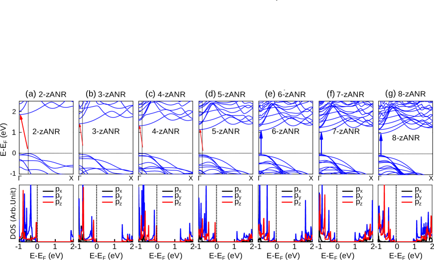
Usually, nanostructuring a semiconducting material into nanoribbons can modulate effectively the gap value () due to the quantum confinement effect x-han ; ad-yoffe ; jw-son . It is true in our case. As can be found in Fig. 2, the amplitude of bandgap in aANRs gradually increases when it goes from 8-aANR to 2-aANR. The gap value scales inversely with the ribbon’s width of , as listed in Tab. I. The increases from 0.79 eV to 1.15 eV with changing from 31.7 Å to 9.5 Å. Besides, it is found that the nature of the bandgap (i.e., direct or indirect) largely depends on the ribbon’s width. An indirect-direct bandgap transition takes place when reducing the ribbon’s width. As shown in Figs. 2(a)-2(c), 2-aANR, 3-aANR and 4-aANR exhibit direct bandgaps. Both the conduction band minimum (CBM) and valence band maximum (VBM) locate at the same crystal point . While in 5-aANR (Fig. 2(d)), 6-aANR (Fig. 2(e)), 7-aANR (Fig. 2(f)) and 8-aANR (Fig. 2(g)), the bandgaps appear as indirect. The CBM is still located at the point while the VBM rises along the -X line and close to the X point. Among the aANRs, direct bandgaps are grasped by the narrower ones with 16.9 Å.
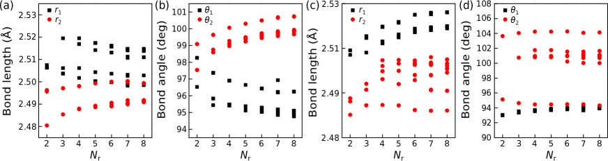
Indeed, such an indirect-direct bandgap transition reflects the structural modifications when arsenene is cut into nanoribbon structures. From inspection of Tab. I, one should have noticed that along with reducing the ribbon’s width, the lattice constant along the infinite direction (denoted as ‘’ in Tab. I) decreases. This consequently affects the bond lengths of and and the bond angles of and . When the ribbon’s width is reduced, increases while decreases (Fig. 4(a)); increases in contrast to decreasing (Fig. 4(b)). As it is found, the increase in one of the bond lengths (or angles) leads to decrease in the other bond length (or angle). At narrower width, both and are more decreased. As a result, the out-of-plane bondings, mainly pz-orbital alike, is strengthened. An decrease in energy is a natural consequence. This effect is clearly demonstrated from the orbital-resolved density of states (DOS), as displayed in the bottom panels in Fig. 2. In the narrower structures, such as 2-aANR (Fig. 2(a)), 3-aANR (Fig. 2(b)) and 4-aANR (Fig. 2(c)), the pz orbitals occupy a lower energy in the valence band (VB) and the VBM is dominated by the py orbitals of in-plane bondings. While in the wider ones from 5-aANR to 8-aANR (see Figs. 2(d)-2(g)), the case is converse. The pz orbitals rise in energy and predominate the VBM. Such a competition between the in-plane and the out-of-plane bondings manipulate the energy gap to be direct or indirect.
By using the nearly free electron model, the effective mass of holes at the VBM () and of electrons at the CBM () are calculated using . In this work, we only concern the and at the point in direct bandgaps. We find that and are comparable in aANRs. In 16.96 Å wide 4-aANR, = 0.24 and = 0.30 ( is the static electron mass). Nanostructuring modifies these values slightly, for example, in the narrowest 9.53 Å wide 2-aANR, = 0.37 and = 0.45.
C. Electronic structures of zANRs
Now, we switch our attention to zANRs. The quantum confinement effect is obviously observed in zANRs. The increases from 1.06 eV to 1.87 eV by decreasing the from 37.7 Å to 8.9 Å (see Tab. I). Strikingly different from the case of aANRs, in zANRs, the indirect-direct bandgap transition happens when increasing the ribbon’s width of . As displayed in Figs. 3(a)-3(d), the bandgaps are indirect in -zANR with 5 ( 23.4 Å). The CBM occurs at the point while the VBM lies along the -X line and close to the point. As the ribbon width is increased up to 28.2 Å, the bandgap turns to be direct with both the CBM and VBM located at the point. Therefore, direct bandgaps hold for the relatively wider zigzag nanoribbons. In contrast to that in aANRs, the values of and in zANRs are relatively larger. In 6-zANR, = 5.96 and = 5.09. While in 8-zANR, = 1.63 and = 1.25.
Similar with that in aANRs, the indirect-direct bandgap transition in zANRs is closely related to the structural changes, as illustrated in Figs. 4(c) and 4(d). By widening the ribbon’s width, the lattice constant along the infinite direction (represented as ‘’ in Tab. I) increases. As a result, the values of and keep almost unchanged; whereas, and are increased. The increase in and will weaken the in-plane covalent bondings and give rise to an energy increase correspondingly. This is why the VBM in the wider structures are predominated by the in-plane py orbitals (from 6-zANR to 8-zANR, see Figs. 3(e)-3(g)). Oppositely, the VBM is occupied by the pz orbitals in the narrower ones from 2-zANR to 5-zANR (see Figs. 3(a)-3(d)). Here also we clearly see the indirect-direct bandgap transition is controlled by a competition between the in-plane and out-of-plane bondings. The mechanism is the same as that discussed above in aANRs. It is that, contracted in-plane bonding parameters ( and ) stabilize the py orbitals in the VB; shrinked out-of-plane bonding parameters ( and ) stabilize the pz orbitals. The relatively higher energy states ultimately dictate the VBM. We should note that these structural changes occur naturally at different ribbon’s widths. Further reducing the parameters by external fields, such as straining, will cause an energy increase, discussed as below.
Based on the above discussion, it is highly expected to achieve direct bandgaps by manufacturing narrow armchair or wide zigzag arsenene nanoribbons. Our results are insightful in consideration of the following two aspects. First, an intrinsic direct bandgap make arsenene applicable in optoelectronics devices. Also, it would be of great interest for valleytronic applications via achieving degenerate energy valleys at different -points kf-mak2 ; t-cao ; sf-wu ; z-zhang2 . Second, the indirect-direct bandgap transition observed in arsenene nanoribbons provides researchers with solid evidence to engineer the bandgap properties of similarly puckered structures or other non-planar structures. Future experiments can test our proposal directly.
D. Electronic structures of aANRs at strains
To further understand the effects of structural changes and engineer the electronic properties of the nanoribbons, strain is applied along the infinite direction of each type of nanoribbons. The magnitude of the strains are employed up to a magnitude of 10%, which is physically realizable considering that it is much lower than the theoretical ultimate strain of the puckered structure c-kamal ; x-peng . We assign the positive (negative) values of for tensile (compressive) strains, respectively. Here, we present the results for 5-aANR and 5-zANR only but similar trends hold for other ribbon widths.
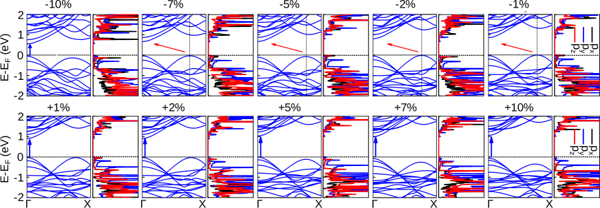
As illustrated in Fig. 5, the armchair structure is particularly sensitive to tensile strains. Although 5-aANR possesses an intrinsic indirect bandgap, a very low tensile strain of = +1% successfully induce a direct bandgap. By contrast, a much higher compressive strain of = -10% is required to make the transition happen. Additionally, tensile strains apparently enhance the bandgap width. As strain is applied between = +1% and = +10%, the bandgap increases from 0.94 eV to 1.12 eV (see Tab. II). In contrast, compressive strain reduces the energy gap. Straining the structure at = -1% and = -10% corresponds to the gap values of 0.86eV and 0.61 eV, respectively.
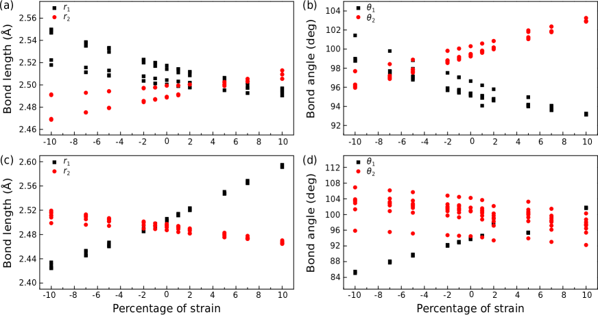
An analysis of the geometric structures is necessary to under the band structures changes. The analysis results are plotted in Figs. 7(a) and 7(b). Both the bond length ( and ) and bond angle ( and ) change linearly with the amount of strain. When straining is applied from = -10% to = +10%, and decrease while and increase. A closer look at the orbital-resolved DOS plots in Fig. 5 reveals that such structural changes makes the VBM is first dominated mainly by px and pz orbitals (from = -10% to = +2%), then by py and pz orbitals (from = +5% to = +7%), and finally by only the py orbitals ( = +10%). As discussed previously, the VBM of 5-aANR under zero strain is comprised of px and pz orbitals (see Fig. 2(d)). Stretching this armchair structure along the armchair direction seems to be capable of stabilizing the px and pz orbitals. Hence, the px and pz orbitals occupy the relative lower energy and the py orbitals dominate the VBM. Similar phenomenon was observed in the similar structure of armchair puckered phosphorene nanoribbons x-han . In addition, at stretching strains, both and is lowered slightly in comparison with the case of no strain (see Tab. II). However, this does not affect the carrier transport property much since the ratio keeps almost unchanged.
E. Electronic structures of zANRs at strains
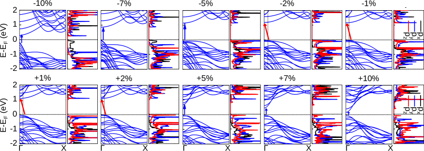
The calculated band structures of 5-zANR at various strains are presented in Fig. 6. We can see that, at a low tensile or compressive strain of 5%, the bandgap remains as indirect. In a contrast, more strengthened stretching ( +5%) or compressing ( -5%) make the bandgap transfer from indirect to direct. In addition to this, in contrast to that in aANRs, both tensile and compressive strains result in decreased bandgaps in 5-zANR (see Tab. II). The gap energy decreases from 1.21eV to 0.24 eV when straining is increased from = 0 to = +10%. The value changes from 1.21eV to 0.32 eV when strain is applied from = 0 to = -10%.
The structural changes of 5-zANR at various strains are plotted in Figs. 7(c) and 7(d). Both the bond length ( and ) and bond angle ( and ) change linearly with the amount of strain. As the strain varies from = -10% to = +10%, and increase while and decrease. This consequently imposes an influence on the electronic states near the VBM. At compressive strains, the VBM is composed mainly with the in-plane bondings of px orbitals (from = -10% to = -7%) and of py orbitals (from = -5% to = -1%). By comparison, at all tensile strains from = +1% to = +10%, the VBM is predominated by the out-of-plane bondings of pz orbitals. This is because that, around the optimized structures, reducing the and causes an energy increase of the in-plane bondings of px and py orbitals; decreasing the and lead to the energy increase of the out-of-plane bondings of pz orbitals, sharing the same mechanism as that in strained aANRs. In addition, straining effectively tune the and , especially the ratio of (see Tab. II). At strains of 0, is much larger than . The ratio of is around 3.7-6.5. In a sharp contrast, at strains of 0, is much smaller than with the ration of = 0.1-0.2.
IV IV. Conclusion
In summary, two types of arsenene nanoribbons are constructed and modeled. An indirect-direct bandgap transition is successfully realized by cutting narrow aANRs and wide zANRs. The indirect-direct bandgap transition is dominated by the competition between the in-plane and out-of-plane bondings. The energy gap of these nanoribbons can be modulated over a wide range by varying the ribbon’s width. Placing aANRs and zANRs under strains significantly modifies the band structures as well as the carrier transport properties. Either stretching or compressing the nanoribbons with an appropriate strength can implement an indirect-direct bandgap transition in both aANRs and zANRs. In addition, in aANRs, the energy gap can be largely enhanced by applying tensile strains. In zANRs, tensile strain results in much larger than while compressive strain makes much smaller than . Our results demonstrate the wide possibilities to tune the electronic properties of two dimensional puckered structures. Further experimental investigations of these structures would be of great interest.
V Acknowledgments
This work was supported by the National Basic Research Program of China under Grant No. 2012CB933101 and the National Science Foundation under Grant No. 51202099.
∗Email: sims@lzu.edu.cn
References
- (1) K. S. Novoselov, A. K. Geim, S. V. Morozov, D. Jiang, M. I. Katsnelson, I. V. Grigorieva, S. V. Dubonos, and A. A. Firsov, Nature 8, 197 (2005).
- (2) M. I. Katsnelson, K. Novoselov, and A. K. Geim, Nat. Phys. 2, 620 (2006).
- (3) D. L. Miller, K. D. Kubista, G. M. Rutter, M. Ruan, W. A. de Heer, P. N. First, and J. A. Stroscio, Science 324, 924 (2009).
- (4) L. Liao, Y.-C. Lin, M. Bao, R. Cheng, J. Bai, Y. Liu, Y. Qu, K. L. Wang, Y. Huang, and X. Duan, Nature 467, 305 (2010).
- (5) Z. Y. Zhang, J. Xie, D. Z. Yang, Y. H. Wang, D. S. Xue, and M. S. Si, arXiv:1411.3165v3 (2014).
- (6) J. Han, J. Xie, Z. Y. Zhang, D. Z. Yang, M. S. Si, and D. S. Xue, arXiv:1501.01425.
- (7) C. Kamal and M. Ezawa, arXiv:1410.5166v1 (2014).
- (8) V. Barone, O. Hod, and G. E. Scuseria, Nano Lett. 6, 2748 (2006).
- (9) M. Y. Han, B. Özyilmaz, Y. Zhang, and P. Kim, Phys. Rev. Lett. 98, 206805 (2007).
- (10) J. Xie, M. S. Si, D. Z. Yang, Z. Y. Zhang, and D. S. Xue, J. Appl. Phys. 1165, 073704 (2014).
- (11) X. Han, H. M. Stewart, S. A. Shevlin, C. R. A. Catlow, and Z. X. Guo, Nano Lett. 14, 4607 (2014).
- (12) L. Tapasztó, G. Dobrik, P. Lambin, and L. P. Biró, Nat. Nanotech. 3, 397 (2008).
- (13) G. Kresse and J. Furthmüller, Comput. Mater. Sci. 6, 15 (1996).
- (14) G. Kresse and J. Furthmüller, Phys. Rev. B 54, 11169 (1996).
- (15) J. P. Perdew, K. Burke, and M. Ernzerhof, Phys. Rev. Lett. 77, 3865 (1996).
- (16) P. E. Blöchl, Phys. Rev. B 50, 17953 (1994).
- (17) A. D. Yoffe, Adv. Phys. 42, 173 (1993).
- (18) J. W. Son, M. L. Cohen, and G. Louie, Phys. Rev. Lett. 97, 216803 (2006).
- (19) K. F. Mak, C. H. Lui, J. Shan, and T. F. Heinz, Phys. Rev. Lett. 102, 256405 (2009).
- (20) T. Cao, J. Feng, J. Shi, and E. Wang, Nat. Commun. 3, 887 (2012).
- (21) S. F. Wu, J. S. Ross, G. B. Liu, G. Aivazian, A. Jones, Z. Fei, W. Zhu, D. Xiao, W. Yao, D. Cobden, and X. Xu, Nat. Phys. 9, 149 (2013).
- (22) Z. Y. Zhang, M. S. Si, Y. H. Wang, X. P. Gao, D. Sung, S. Hong and J. He, J. Chem. Phys. 140, 174707 (2014).
- (23) X. Peng and Q. Wei, Appl. Phys. Lett. 104, 251915 (2014).


| aANRs | zANRs | |||||
|---|---|---|---|---|---|---|
| 2 | 9.5 | 4.39 | 1.15d | 8.9 | 3.63 | 1.87i |
| 3 | 13.3 | 4.51 | 0.99d | 13.7 | 3.64 | 1.48i |
| 4 | 16.9 | 4.57 | 0.94d | 18.6 | 3.65 | 1.33i |
| 5 | 20.6 | 4.60 | 0.90i | 23.4 | 3.66 | 1.21i |
| 6 | 24.3 | 4.63 | 0.85i | 28.2 | 3.66 | 1.15d |
| 7 | 28.1 | 4.65 | 0.80i | 32.9 | 3.66 | 1.07d |
| 8 | 31.7 | 4.66 | 0.79i | 37.7 | 3.67 | 1.06d |
| 5-aANR | 5-zANR | |||||
|---|---|---|---|---|---|---|
| (eV) | (eV) | |||||
| +10% | 1.12d | 0.19 | 0.21 | 0.24d | 0.41 | 0.11 |
| +7% | 1.07d | 0.20 | 0.23 | 0.51d | 0.53 | 0.10 |
| +5% | 1.03d | 0.20 | 0.24 | 0.71d | 0.65 | 0.10 |
| +3% | 0.96d | 0.21 | 0.26 | 1.13i | N/A | N/A |
| +1% | 0.94d | 0.22 | 0.27 | 1.17i | N/A | N/A |
| 0 | 0.90i | N/A | N/A | 1.21i | N/A | N/A |
| -1% | 0.86i | N/A | N/A | 1.19i | N/A | N/A |
| -3% | 0.82i | N/A | N/A | 1.20i | N/A | N/A |
| -5% | 0.77i | N/A | N/A | 1.20d | 0.13 | 1.24 |
| -7% | 0.70i | N/A | N/A | 0.92d | 0.12 | 1.23 |
| -10% | 0.61i | 0.31 | 0.42 | 0.32d | 0.19 | 1.20 |