Observation of the symmetry of core states of a single Fe impurity in GaAs
Abstract
We report the direct observation of two mid-gap core states of differing symmetry for a single Fe atom embedded in GaAs. These states are distinguished by the strength of their hybridization with the surrounding host electronic structure. The mid-gap state of Fe that does not hybridize via bonding is strongly localized to the Fe atom, whereas the other, which does, is extended and comparable in size to other acceptor states. Tight-binding calculations of these mid-gap states agree with the spatial structure of the measured wave functions, and illustrate that such measurements can determine the degree of hybridization via bonding of impurity states. These single-dopant mid-gap states with strong character, which are intrinsically spin-orbit-entangled, provide an opportunity for probing and manipulating local magnetism and may be of use for high-speed electrical control of single spins.
The electronic localization of single dopant states within the electronic energy gap of a host semiconductor provides a model pseudo-atomic system to manipulate in an effective semiconductor “vacuum”Koenraad and Flatté (2011); Steger et al. (2012). Recent progress in single-dopant measurement and manipulation has included optical and electronic addressing of individual spin centersJelezko and Wrachtrup (2006); Balasubramanian et al. (2009), observation of virtual internal transitions among mid-gap statesBocquel et al. (2013), valley-orbit couplingZwanenburg et al. (2013), and the effects of strain on the symmetry of the electronic wave functionsYakunin et al. (2007); Doherty et al. (2012). An individual transition-metal dopant in a tetrahedrally-bonded semiconductor can provide access to most of these phenomenaTang et al. (2006); Yakunin et al. (2007); Chanier et al. (2012). In addition, the potential for very large impurity spin-orbit and exchange interactions has suggested new ways to probeTang and Flatté (2005) and manipulate local spins and magnetic properties using electric fieldsTang et al. (2006), strainYakunin et al. (2007), or a surfaceStrandberg et al. (2011). For a specific single substitutional transition-metal dopant in a tetrahedrally-bonded semiconductor, the electronic structure of the mid-gap states are governed by charge-transfer energies, -state filling, and the compatibility of -orbital symmetry with the bonding in the surrounding hostKikoin and Fleurov (1994); McCluskey and Haller (2012). In the absence of spin-orbit splitting, the states of a substitutional impurity split in the crystal field into two types of states with very different symmetry relative to the host; so-called and states. The states have the same symmetry in the crystal field as the orbitals, and hence hybridize efficiently with them along the bonds connecting the impurity to its four nearest neighbors. The states, in contrast, have an incompatible symmetry with the orbitals via bonding, but could hybridize through the much weaker bonding, or through bonding and spin-orbit mixing, to the four nearest neighbors. To date the acceptor features seen for acceptors in tetrahedrally-bonded semiconductorsZheng et al. (1994a, b); de Kort et al. (2001); Yakunin et al. (2004); Kitchen et al. (2006); Jancu et al. (2008); Richardella et al. (2009); Bocquel et al. (2013); Mühlenberend et al. (2013) have all been associated with symmetry, including Zn, Mn, Co and Fe.
Here we report the direct observation with scanning tunneling microscopy (STM) and scanning tunneling spectroscopy (STS) of states that have symmetry and hybridize with the surroundings, around a single sub-surface Fe impurity substituted for a Ga atom below the (110) surface of GaAs. The hybridization is very weak for these states compared to the previously-observed states, which manifests in a much more localized apparent wave function for the state than the simultaneously-observed state around the same Fe impurity. A theoretical description of the electronic states requires a technique that can describe the wave function on tens of thousands of atoms while preserving the local orbital symmetry in the basis; this description can be implemented in an tight-binding theory that describes the electronic structure of the host using an empirical basisChadi (1977); Tang and Flatté (2004); Mahani et al. (2014), and matches the levels of the impurity from ab initio calculations, consistent with experimental measurements. With this approach, the theoretical calculations show excellent agreement with the spatial structure of the states, and by ignoring - hybridization between the Fe and the surrounding As atoms, provides excellent agreement for the spatial structure of the states. The penetration of states of an Fe impurity into the surrounding GaAs, even in the absence of hybridization, also suggests that the hybridization of rare-earth dopants with a surrounding tetrahedrally-bonded host may be observable.
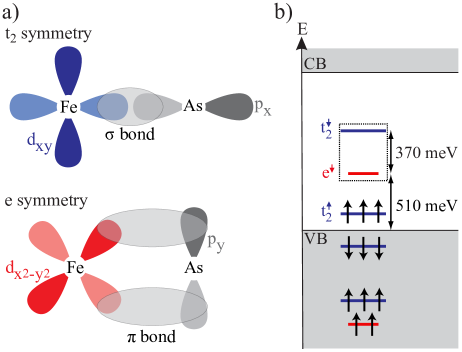
The spatial structure of the and orbitals of a transition-metal atom in a tetrahedrally-bonded semiconductor, and the symmetry of the orbital overlaps with orbitals on the neighboring As atoms in the absence of spin-orbit interactions, are shown in Fig. 1(a). The electronic configuration of the free atom is [Ar] with electrons in the shell. In order to replace a cation with an electronic configuration and act as an isoelectronic impurity in the host crystal, a transition-metal atom M should release 3 electrons of which two are 4 electrons and one is a 3 electron. The electronic configuration becomes M3+ (dn-1) with electrons in the d-shell. The 3 shell is partially filled and the 4 states form the outermost shell. Fig. 1(b) shows the energies of the resulting features in the spectrum, with a dashed black frame around the and features investigated in this paper. The different transition energies shown in this diagram were determined by optical spectroscopy Malguth et al. (2008); Pressel et al. (1993).
These and states are observed in cross-sectional STM (X-STM) performed at 5 K under UHV conditions (510-11 Torr). Several electrochemically etched tungsten STM tips were used. The STM was operated in constant current mode on a clean and atomically flat GaAs (110) surface obtained by in situ cleavage. The molecular beam epitaxy grown sample contains a 100 nm Fe-doped GaAs layer (nominal concentration of 21018 cm-3) and an Fe monolayer incorporated in GaAs. The growth temperature was 480oC during the entire growth procedure. The nominal layer structure consisted of GaAs substrate/100 nm Fe:GaAs/200 nm GaAs/Fe monolayer/500 nm GaAs. The two Fe-doped regions are co-doped with C atoms (nominal concentration of 21018 cm-3). These shallow acceptors greatly increase the conductivity at the experiment’s temperature of 5 K, while having little influence on the position of the sample Fermi level (which is in the gap, close to the top of the valence band).
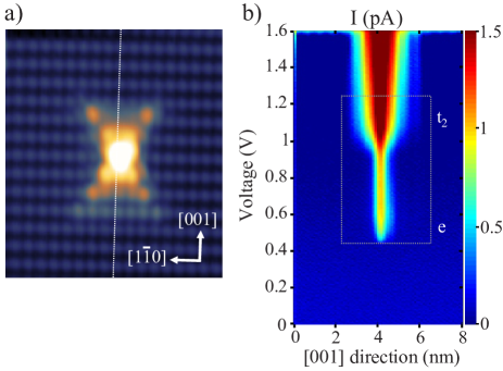
The empty-states topography image of single sub-surface Fe impurity shown in Fig. 2(a) presents a bright and anisotropic contrast. This feature shows a strong similarity with the contrast reported for the sub-surface [Mn2++h+] neutral acceptor state Yakunin et al. (2004). Both contrasts share common features like their brightness and their anisotropic shape. The anisotropic shape, clearly visible at low voltages, fades away at higher voltages as reported for other acceptorsYakunin et al. (2004). This evolution is not completely gradual. Above V=+1.7 V, the anisotropic shape disappears for the most part, leaving only a bright localized contrast, while a clear change in corrugation of the GaAs surface is observed. This is explained by the contribution of empty conduction band states above V=+1.7 V, which overwhelms the smaller local density of states of the mid-gap states .
The bright electronic contrast of the Fe atom is perfectly symmetric with respect to the [001] axis and highly symmetric with respect to the [10] axis. In the case of Mn atoms in GaAs, it has been shown that the degree of asymmetry with respect to the [10] axis is related to the interaction between the Mn state with the asymmetric buckled surfaceÇelebi et al. (2010), and similar effects have been identified for Mn in InAsMarczinowski et al. (2007); Loth et al. (2008). Consequently, the symmetry decreases as the impurities approach closer to the surface. Similar depth dependence is observed for Fe impurities. The low Fe concentration achieved in each sample did not allow for a systematic study of Fe impurities at different depths. Nonetheless, a qualitatively similar depth dependance to Mn is observed for Fe, even if each impurity could not be unambiguously attributed to a specific depth. We estimate the Fe dopant shown in Fig. 2 to be two or three monolayers below the surface.
The Fe atoms in the first monolayers exhibit a higher degree of symmetry with respect to the [10] direction than is seen for Mn atoms. The higher binding energy and weaker hybridization expected for Fe states with the host crystal explains this difference. In addition the surface, and the strain it produces, does not affect the wave functions of these Fe states significantly as they are more localized. Studies of the dependence of the wavefunction symmetry on acceptor binding energy indicate that the deeper the acceptor level the more symmetric it appearsÇelebi et al. (2008). The deep acceptor states of Fe are thus expected to possess a stronger impurity character than the Mn acceptor states.
In the STM experiment, at positive bias voltages, electrons are injected in the empty states of the semiconductor sample, that is into the conduction band and the empty energy levels associated with Fe impurities. In these conditions, the semiconductor’s bands bend upwards due to tip induced band bending (TIBB)Feenstra et al. (2002); Yakunin et al. (2004). The Fermi level in the bulk is in the gap, close to the top of the valence band, therefore the deep and levels, located 510 meV and 880 meV above the valence band edge respectively, are empty. The majority-spin level is occupied. Thus the energy level occupation of Fig. 1(b), which corresponds to the electronic configuration of the Fe3+ isoelectronic acceptor state, applies. This implies that electrons tunneling through the deep and levels are responsible for the bright electronic contrast observed in the empty-states images. The anisotropic shape is solely attributed to the core level wave function, as the level is expected to have a much more localized contrast. Comparing STM height profiles taken across the neutral Mn and Fe impurities shows that, in the case of Fe, the enhancement of the LDOS is more localized on the impurity itself. This is consistent with the deep nature of the Fe3+ isoelectronic acceptors levels as well as the additional and localized tunneling channel due to the presence of an state in the bandgap for Fe. This explains why only Fe atoms a few monolayers from the surface can be resolved.
The validity of the analysis above is supported by further experimental and theoretical investigations. A spatially resolved I-V spectroscopy experiment at 5 K was performed to study a single sub-surface Fe impurity. The data acquisition was set such that the tip-sample distance was the same for every point. This is achieved by moving the tip with the feedback loop on at a voltage at which the topography is uniform across the whole image (here V=+2.5 V). At each point, I-V curves were taken after the tip had been brought closer to the surface by 0.2-0.5 nm with the feedback loop off. These settings are chosen to avoid any topography cross-talk in the spatial resolved I-V spectroscopy data.
A 7.5 nm wide cross-section taken across the subsurface Fe impurity along the [001] direction is shown in Fig. 2(b) for voltages between 0 V and 1.6 V. Each curves has been numerically derived from the I-V curves recorded experimentally, after subtracting the offset induced by the I-V converter. This plot shows two distinct peaks around +0.5 V and +1.0 V, which are attributed to and acceptor states related to Fe, while the onset of the conduction band is visible at a voltage of 1.55 V. The fact that the signal does not drop directly to zero at energies above these two peaks is attributed to the tunneling from states below the Fermi energy in the tip.
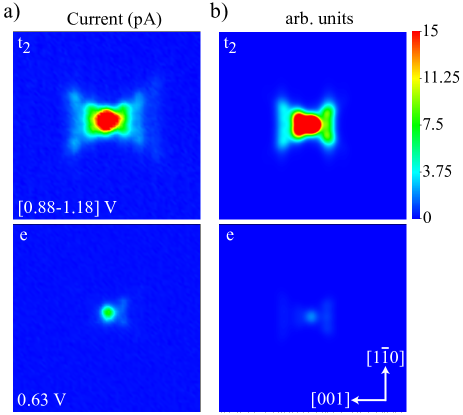
The spatial structure of these features can be most clearly seen by considering the maps taken at 0.63 V and coming from the [0.88-1.18] V bias window, corresponding to the energy positions associated with the largest contributions to the two peaks. These are presented in Fig. 3(a) in the bottom and top panels, respectively. The spatial extent of these two states is clearly different. The lower-energy state is strongly localized on the Fe impurity itself. The wave function of this state is almost isotropic and extends over 0.75 nm. Two small features can be seen extending in the [00] direction. The higher localization of this state is explained by the weak hybridization of the states with states of the host crystal, due to an incompatibility of -like orbitals with host orbitals [Fig. 1(a)]. The higher energy state presents extensions into the host semiconductor in a cross-like shape. The wave function of this state is anisotropic and extends over 2.5 nm along the [001] direction and 2 nm along the [10] direction.
These features are well reproduced by a tight-binding calculation, shown in Fig. 3(b). We calculate the Green’s functions for bulk GaAs using an tight-binding descriptionChadi (1977). The effect of the impurity is evaluated using a Koster-Slater techniqueKoster and Slater (1954) similar to that used to determine the acceptor state wave function for Mn in GaAsTang and Flatté (2004). Here orbitals are added to the Fe impurity site in the calculations, and the -orbital energies and hopping matrix elements are introduced. The -orbital energies are determined from experimental measurements of the Fe mid-gap statesMalguth et al. (2008); Pressel et al. (1993). As the orbitals on the Fe are , whereas those included in tight-binding descriptions of GaAsChadi (1977) are , the hopping parameters must be determined separately. We set the hopping to be zero, based on the symmetry arguments of Fig. 1(a), so there is a single fit parameter in the theory, the hopping, which is set based on the spatial extent of the state. The hopping between Fe and As should be much smaller than that between Ga and As states, and the optimal value we determine, eV, is two orders of magnitude smaller than that parametrized for hopping in GaAsJancu et al. (1998). Once the extent of the state is set, the extent of the state is determined without adjustable parameters; the LDOS beyond the position of the Fe results from a small contribution originating from the spin-orbit interaction. Fig. 3(b) presents the calculated real space probability density of the states of (top) and (bottom) symmetry taken for a cut through the bulk GaAs crystal 3 layers away from the Fe ion. The shapes of the calculated LDOS are in general agreement with the experimental wavefunctions and the calculated LDOS is concentrated heavily on the impurity itself. The latter result is consistent with the experimental STM height profile taken above single Fe impurities.
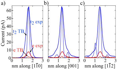
Agreement is also evident in Fig. 4 for line cuts along three directions. Here the spatial resolution of the theoretical calculation has been set to be sharper than the experiment so that the origin of the shoulders of the line cuts can be more clearly seen. They originate from the amplitude of the state on neighboring atoms.
The features observed here differ greatly from those measured for Fe in the surface layerRichardella et al. (2009); Mühlenberend et al. (2013). For Fe in the surface layer the two peaks found at 0.88 eV and 1.5 eV were interpreted as corresponding to splitting of the states due to symmetry-breaking at the surface. Their results are supported by the odd and even spatial symmetry, and similar spatial extent, of the two states appearing in the differential conductance maps at the corresponding energiesRichardella et al. (2009). Impurity states at the surfaceLee and Gupta (2011); Garleff et al. (2011) are known to be quite different from those even a layer below the surface, which are much less sensitive to the influence of the surfaceGarleff et al. (2008, 2010). The two states in our Figs. 3 and 4 do not exhibit the even and odd symmetry expected for states resulting from a splitting of the state by the effect of the reconstructed surface. Instead, the shape and the spatial extent of these states are consistent with that expected, and calculated theoretically, if the states are not split.
Acknowledgements.
We acknowledge support from the European Community’s Seventh Framework Programme (PF7/2007-2013) SemiSpinNet and an AFOSR MURI. J. B. and V. R. K. contributed equally to this work.References
- Koenraad and Flatté (2011) P. M. Koenraad and M. E. Flatté, Nature Materials 10, 91 (2011).
- Steger et al. (2012) M. Steger, K. Saeedi, M. L. W. Thewalt, J. J. L. Morton, H. Riemann, N. V. Abrosimov, P. Becker, and H.-J. Pohl, Science 336, 1280 (2012).
- Jelezko and Wrachtrup (2006) F. Jelezko and J. Wrachtrup, Phys Status Solidi A 203, 3207 (2006).
- Balasubramanian et al. (2009) G. Balasubramanian, P. Neumann, D. Twitchen, M. Markham, R. Kolesov, N. Mizuochi, J. Isoya, J. Achard, J. Beck, J. Tissler, V. Jacques, P. R. Hemmer, F. Jelezko, and J. Wrachtrup, Nature Materials 8, 383 (2009).
- Bocquel et al. (2013) J. Bocquel, V. R. Kortan, C. Şahin, R. P. Campion, B. L. Gallagher, M. E. Flatté, and P. M. Koenraad, Phys. Rev. B 87, 075421 (2013).
- Zwanenburg et al. (2013) F. A. Zwanenburg, A. S. Dzurak, A. Morello, M. Y. Simmons, L. C. L. Hollenberg, G. Klimeck, S. Rogge, S. N. Coppersmith, and M. A. Eriksson, Rev. Mod. Phys. 85, 961 (2013).
- Yakunin et al. (2007) A. M. Yakunin, A. Y. Silov, P. M. Koenraad, J.-M. Tang, M. E. Flatté, J.-L. Primus, W. Van Roy, J. De Boeck, A. M. Monakhov, K. S. Romanov, I. E. Panaiotti, and N. S. Averkiev, Nature Materials 6, 512 (2007).
- Doherty et al. (2012) M. W. Doherty, F. Dolde, H. Fedder, F. Jelezko, J. Wrachtrup, N. B. Manson, and L. C. L. Hollenberg, Phys. Rev. B 85, 205203 (2012).
- Tang et al. (2006) J.-M. Tang, J. Levy, and M. E. Flatté, Phys. Rev. Lett. 97, 106803 (2006).
- Chanier et al. (2012) T. Chanier, C. Pryor, and M. E. Flatté, Phys. Rev. B 86, 085203 (2012).
- Tang and Flatté (2005) J.-M. Tang and M. E. Flatté, Phys. Rev. B 72, 161315(R) (2005).
- Strandberg et al. (2011) T. O. Strandberg, C. M. Canali, and A. H. MacDonald, Phys. Rev. Lett. 106, 017202 (2011).
- Kikoin and Fleurov (1994) K. A. Kikoin and V. N. Fleurov, Transition Metal Impurities in Semiconductors (World Scientific, New York, 1994).
- McCluskey and Haller (2012) M. D. McCluskey and E. E. Haller, Dopants and Defects (CRC Press, New York, 2012).
- Zheng et al. (1994a) Z. F. Zheng, M. B. Salmeron, and E. R. Weber, Applied Physics Letters 64, 1836 (1994a).
- Zheng et al. (1994b) Z. F. Zheng, M. B. Salmeron, and E. R. Weber, Applied Physics Letters 65, 790 (1994b).
- de Kort et al. (2001) R. de Kort, M. C. M. M. van der Wielen, A. J. A. van Roij, W. Kets, and H. van Kempen, Phys. Rev. B 63, 125336 (2001).
- Yakunin et al. (2004) A. M. Yakunin, A. Yu. Silov, P. M. Koenraad, W. Van Roy, J. De Boeck, J. H. Wolter, J.-M. Tang, and M. E. Flatté, Phys. Rev. Lett. 92, 216806 (2004).
- Kitchen et al. (2006) D. Kitchen, A. Richardella, J.-M. Tang, M. E. Flatté, and A. Yazdani, Nature 442, 436 (2006).
- Jancu et al. (2008) J.-M. Jancu, J.-C. Girard, M. O. Nestoklon, A. Lemaître, F. Glas, Z. Z. Wang, and P. Voisin, Physical Review Letters 101, 196801 (2008).
- Richardella et al. (2009) A. Richardella, D. Kitchen, and A. Yazdani, Physical Review B 80, 045318 (2009).
- Mühlenberend et al. (2013) S. Mühlenberend, M. Gruyters, and R. Berndt, Phys. Rev. B 88, 115301 (2013).
- Chadi (1977) D. J. Chadi, Phys. Rev. B 16, 790 (1977).
- Tang and Flatté (2004) J.-M. Tang and M. E. Flatté, Phys. Rev. Lett. 92, 047201 (2004).
- Mahani et al. (2014) M. R. Mahani, M. F. Islam, A. Pertsova, and C. M. Canali, Phys. Rev. B 89, 165408 (2014).
- Malguth et al. (2008) E. Malguth, A. Hoffmann, and M. R. Phillips, Physica Status Solidi (B) 245, 455 (2008).
- Pressel et al. (1993) K. Pressel, A. Dornen, G. Ruckert, and K. Thonke, Physical Review B 47, 16267 (1993).
- Çelebi et al. (2010) C. Çelebi, J. K. Garleff, A. Silov, A. Yakunin, P. M. Koenraad, J.-M. Tang, and M. E. Flatté, Physical Review Letters 104, 086404 (2010).
- Marczinowski et al. (2007) F. Marczinowski, J. Wiebe, J.-M. Tang, M. E. Flatté, F. Meier, M. Morgenstern, and R. Wiesendanger, Physical Review Letters 99, 157202 (2007).
- Loth et al. (2008) S. Loth, M. Wenderoth, and R. G. Ulbrich, Phys. Rev. B 77, 115344 (2008).
- Çelebi et al. (2008) C. Çelebi, P. M. Koenraad, A. Y. Silov, W. V. Roy, A. M. Monakhov, J.-M. Tang, and M. E. Flatté, Physical Review B 77, 075328 (2008).
- Feenstra et al. (2002) R. M. Feenstra, G. Meyer, F. Moresco, and K. H. Rieder, Phys. Rev. B 66, 165204 (2002).
- Koster and Slater (1954) G. F. Koster and J. C. Slater, Phys. Rev. 95, 1167 (1954).
- Jancu et al. (1998) J.-M. Jancu, R. Scholz, F. Beltram, and F. Bassani, Phys. Rev. B 57, 6493 (1998).
- Lee and Gupta (2011) D. Lee and J. Gupta, Nano Letters 11, 2004 (2011).
- Garleff et al. (2011) J. Garleff, A. Wijnheijmer, C. N. v. d. Enden, and P. Koenraad, Physical Review B 84, 075459 (2011).
- Garleff et al. (2008) J. Garleff, C. Çelebi, W. Van Roy, J.-M. Tang, M. Flatté, and P. Koenraad, Physical Review B 78, 075313 (2008).
- Garleff et al. (2010) J. K. Garleff, A. P. Wijnheijmer, A. Y. Silov, J. van Bree, W. Van Roy, J.-M. Tang, M. E. Flatté, and P. M. Koenraad, Phys. Rev. B 82, 035303 (2010).