Artificial Gauge Field and Quantum Spin Hall States in a Conventional Two-dimensional Electron Gas
Abstract
Based on the Born-Oppemheimer approximation, we divide total electron Hamiltonian in a spin-orbit coupled system into slow orbital motion and fast interband transition process. We find that the fast motion induces a gauge field on slow orbital motion, perpendicular to electron momentum, inducing a topological phase. From this general designing principle, we present a theory for generating artificial gauge field and topological phase in a conventional two-dimensional electron gas embedded in parabolically graded GaAs/InxGa1-xAs/GaAs quantum wells with antidot lattices. By tuning the etching depth and period of antidot lattices, the band folding caused by superimposed potential leads to formation of minibands and band inversions between the neighboring subbands. The intersubband spin-orbit interaction opens considerably large nontrivial minigaps and leads to many pairs of helical edge states in these gaps.
pacs:
71.70.Ej, 75.76.+j, 72.25.MkI INTRODUCTION
Exploring of various topological quantum states is always one of the central issue of condensed matter physics TQS1 ; TQS2 ; TQS3 . Topological insulators (TIs) RMP1 , a new class of solids, posses unique properties such as robust gapless helical edge or surface states and exotic topological excitations RMP1 ; RMP2 ; Kane ; BHZ ; Konig1 ; Konig2 ; Fu ; Fu2 ; Hsieh ; ZXShen ; Hasan ; Lin ; Franz ; KYang ; Chadov ; Heusler ; Chang1 ; Chang2 ; Chang3 ; GaAs ; Oxide ; Tinfilm ; Franz2 ; Katsnelson . The helical edge states of two-dimensional (2D) TIs are protected strictly against elastic backscattering from nonmagnetic impurities. This feature leads to dissipationless conducting channels and therefore is promising for possible applications in spintronics, quantum information, thermoelectric transport and on-chip interconnection in integrated circuit. These novel applications require large nontrivial gaps, which suppress the coupling between the edge and bulk states, leading to dissipationless edge transport. For this purpose, there is an ongoing search for feasible realizations of various narrow gap materials containing heavy elements, e.g., CdTe/HgTe/CdTe quantum wells (QWs) BHZ ; Konig1 ; Konig2 , and Tin film Tinfilm . However, fabrication of high-quality samples of these proposed structures still remains a challenging task, requiring precise control for material growth.
In this work, we demonstrate that conventional semiconductor GaAs/InxGa1-xAs/GaAs two-dimensional electron gas (2DEG) with antidot lattices can be driven into the TI phase. The 2DEGs provide a promising playground for realizing TI states with quite large nontrivial gap ( meV) operating at liquid nitrigen temperature regime, instead of searching new materials containing heavy atoms. We first present a general analysis for generating an artificial gauge field in a semiconductor 2DEG, then we demonstrate band inversion between neighboring subbands utilizing antidot lattices created by well-developed semiconductor etching technique, and generate the TI phase with many pairs of helical edge states. This suggests a completely new method to generate topological phase in conventional semiconductor 2DEGs without strong spin-orbit interaction (SOI), at liquid nitrigen temperature regime.
II GAUGE FIELD FROM BORN-OPPENHEIMER APPROXIMATION
First we discuss the emergence of an artificial gauge field in a system of electrons in a 2D system described by a low-energy single-particle Hamiltonian , where and are Pauli matrices describing the electron spin and the conduction () and valence () bands, respectively, and are identity matrices. Taking , , and other , we obtain the Bernevig-Hughes-Zhang (BHZ) Hamiltonian for 2D TIs BHZ . Neglecting the band index , and taking , , , we get the Hamiltonian for a 2DEG with Rashba and Dresselhaus SOIs, where and are the strengths of Rashba and Dresselhaus SOIs, respectively. Next, we divide the total Hamiltonian into the intra-band, slow part and the inter-band, fast part , which usually arises from the SOIs in real materials. The eigenstate of the total Hamiltonian can be decomposed into the fast and slow components: , where are eigenstates of the fast part and describe the slow part. The fast spin dynamics compared with the slow orbital motion allow us to make the Born-Oppenhenmer approximation, i.e., neglecting the coupling between different , and derive an effective Hamiltonian governing the slow orbital motion (see Appendix A):
| (1) |
where acts as an effective potential that seperates different bands and is a gauge potential in the momentum space of the slow orbital motion, due to the interband coupling to the fast spin dynamics Wilczek ; CPSun . For the BHZ Hamiltonian, the gauge potential leads to an effective Lorentz force in the momentum space perpendicular to the electric field :
| (2) |
where denotes spin up or down state while denotes the conduction or valence band, respectively (). The Chern number is obtained by integrating the field strength in the Brillouin zone. The sign change in would induce a change of the Chern number by 1, which corresponds to the topological phase transition Moore ; Galitski .
For a 2DEG with Rashba and Dresselhaus SOIs, we find , which means that the Chern number vanishes in 2DEG with SOIs. Comparing the Hamiltonian of 2D TIs to that of 2DEGs with SOIs, one can see clearly that 2D TIs posses an additional degree of freedom: the band index . In order to generate the gauge field and realize TI phases in a 2DEG, one needs to create minibands and band inversion in 2DEGs.
III EFFECTIVE HAMILTONIAN AND QUANTUM SPIN HALL STATES
Based on the above designing principle, we will create topological phase in conventional semiconductor 2DEG. This is the first demonstration of the formation of a TI phase in the s-like band systems, i.e., a 2DEG with nanostructured antidot lattice shown schematically in Fig. 1(a). Nanostructured antidot lattices, consisting of periodically arranged holes that are etched in a 2DEG, form a strongly repulsive egg-carton-like periodic potential in a 2DEG Antidot ; Antidot1 ; Antidot2-1 ; Antidot2-2 ; Antidot3-1 ; Antidot3-2 ; Antidot4 ; Antidot5 . This artificial crystals lead to a wide variety of phenomena, for instance, Weiss oscillation, chaotic dynamics of electrons, the formation of an electronic miniband structure and massless Dirac fermions. At low temperatures, the mean free path of electrons is much longer than the period of antidot lattices ranging from 10 to 100 nanometers. The modulated periodic potential can also be created by electron beam lithography electrodeposition and periodic arrays of metallic nanodots can be realized on semiconductor surfaces. Due to elastic strains producing these dots, a sufficiently strong piezoelectric potential modulation results in miniband effects in the underlying 2DEG Antidot2-1 ; Antidot2-2 . Very recently, a honeycomb lattice of coronene molecules was created by using a cryogenic scanning tunneling microscope on a Cu(111) surface to construct artificial graphene-like lattice with the lattice constant approaching nm Antidot5 .
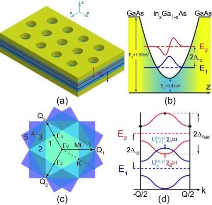
We consider the 2DEG in a GaAs/InxGa1-xAs/GaAs PQW, which was fabricated successfully before paraQW1-1 ; paraQW1-2 ; paraQW2 , with a triangular antidot lattice (see Fig. 1(a)). Before going to the numerical calculation, we first give a clear physical picture for the emergence of a TI phase in this 2DEG system upon nanostructuring with antidot lattice. The simplest description of the 2DEG system is obtained by reducing the eight-band Kane model to the lowest conduction subbands of the QW (see Appendix B). This gives the Hamiltonian for the 2DEG with periodic antidot lattice potential :
| (3) |
where are Pauli matrices describing the first and second QW subbands of effective mass , and refer to the electron spin. The second term comes from the energy difference between the first and second subbands [see Fig. 1(b)]. The third term describes the inter-subbands SOI (ISOI) obtained from the eight-band Kane model using the Löwdin perturbation theory (see Appendix B). The coupling strength is
| (4) |
where and are the band gap and spin split-off splitting in the QW region, , and is the Kane matrix element. The SOIs in 2DEGs usually come from the asymmetry of the QWs, i.e., Rashba SOI. Surprisingly, the ISOI can appear in a symmetric PQW, behaving like a hidden SOI. From Eq. (4), one can see that the ISOI arises from the spatial variations of the bandgap , the Kane matrix , and the intrinsic SOI , i.e., the variation of the concentration of In component, which behaves like an effective local electric field. This local electric field would not push the electron and the hole states to the left and right sides of the QW, but it can induce a considerably large ISOI hidden in symmetric QWs. The initial and final states are neighboring subbands having opposite parity, while the variations of , and in a symmetric QW are odd. This means that the ISOI can exist in symmetric QWs.
The first and second subbands both form minibands due to the Brillouin zone folding caused by the antidot lattice. The band inversion could occur between the two adjacent minibands of the first subband and the second subband (see Fig. 1(d)), where is the th miniband formed by the antidot lattice. We model the triangular antidot lattice potential by a periodic potential with potential height , , , and is the triangular antidot lattice constant (see Appendix C).
To describe the four minibands (two spin-degenerate minibands) , , , involved in the band inversion, we treat other electron and hole minibands by Löwdin perturbation theory and reduce the eight-band Kane kp model to the following effective Hamiltonian within the basis (, , , ):
| (5) |
(see Appendix D and E), which assumes the same form as the BHZ Hamiltonian. Here , [see Fig. 1(b)], , and characterize the ISOI strength between neighboring minibands with opposite spin. This Hamiltonian obviously has a topological phase when , corresponding to band inversion.
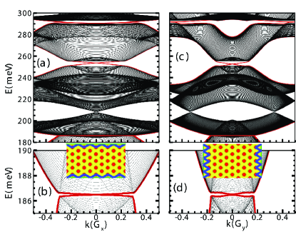
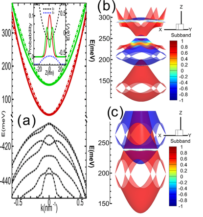
Next we employ the eight-band Kane kp model to calculate the subband structure with SOIs in a 40-nm-thick GaAs/InxGa1-xAs/GaAs PQWs paraQW1-1 ; paraQW1-2 , as plotted in Fig. 2(a). The energy difference between the minima of the first and second subbands at point is about 90 meV [see Fig. 2(a)]. In order to calculate the miniband structures caused by an in-plane periodic potential induced by the triangular antidot lattice, we reduce the eight-band model to an effective four-band kp Hamiltonian by including the lowest 20 electron subbands and 54 highest hole subbands in the QW, to reproduce the energy dispersions of the first and second subbands calculated from the eight-band Kane model [see Fig. 2(a)]. The parameters in the four-band Hamiltonian is given in Appendix E. The minibands from the four-band kp Hamiltonian are shown in Figs. 2(b) and 2(c). These minibands originates from folding the first and second subbands of the QW into the first Brillouin zone of the antidot lattice [Fig. 1(c)]. By tuning the antidot lattice constant and the potential height , i.e., the etching depth of the antidot lattice, many band inversions appear between these minibands, which can be clearly seen in Figs. 2(b) and 2(c). The minigaps between these minibands are opened by the ISOI shown in Eq. (4) [see Figs. 2(b) and 2(c)].
To demonstrate that these minigaps are topologically nontrivial, we determine the parity of each miniband at the four time-reversal invariant momenta Fu2 () in the first Brillouin zone shown in Fig. 1(c). For the lowest spin-degenerate minibands being occupied, the invariant is given by , where is the parity of the th occupied miniband at . Our calculation gives at all the minigaps, which proves the whole system is in the quantum spin-Hall phase (see Appendix F).
Next, we demonstrate the emergence of topological edge states upon etching the QW into a Hall bar structure along two different directions ( axis and axis). As shown in Fig. 3, a pair of topological helical edge states appear inside each nontrivial minigap. For example, we can see topological helical edge states in the lowest two nontrivial minigaps near meV and meV, respectively. The helical edge state pairs in these minigaps would lead to higher conductance plateaus as the Fermi energy increases by increasing the doping level. The helical edge states do not overlap with the bulk states, making it possible to be detected experimentally.
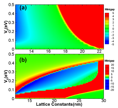
The lowest nontrivial minigaps is quite small (about meV), but the second minigap is larger (about meV). By tuning the period and potential height of the antidot lattice, the nontrivial minigaps can be significantly enhanced [see Figs. 4(a) and 4(b)]. For example, the lowest minigaps can be enhanced to meV, which is already comparable with that in HgTe and InAs/GaSb QW systems ( meV) Konig1 ; Konig2 . The second minigaps can approach meV, which means the TI phase can be realized at liquid nitrigen temperature regime. From Figs. 4(a) and 4(b), one can see that the lowest nontrivial minigap is closed as the lattice constant increases, but the second higher nontrivial minigap survives, i.e., the TI phase can exist even at large lattice constants, e.g., nm.
Finally, we comment on the experimental detection the aforementioned edge states in GaAs/InxGa1-xAs/GaAs quantum Hall bar (shown schematically in the insets of Figs. 3(b) and 3(d)). One way to detect the aforementioned edge states (shown in Fig. 3) is the standard four terminal measurements as demonstrated in previous works Konig1 ; Konig2 . In contrast to HgTe and InAs/GaSb QW systems, there are many pairs of helical edge states in our system between these inverted minibands, which leads to higher plateaus with increasing the Fermi energy. Another possible way is microwave impedance microscopy which makes spatial-resolved nano-scale images ( 100 nm) of the conductivity and permittivity of a sample MIM . The unoccupied edge states in higher minigaps can be detected using the angle-resolved photonemission technique ARPAS2013 , which has already been successfully applied to identify occupied and unoccupied surface states in Bi2Se3 and Bi2TexSe3 ARPAS1999 ; ARPAS2012 ; ARPAS2013 .
IV CONCLUSION
Our proposal is based on a general analysis about the electron orbital motion in TIs. By using the Born-Oppenheimer approximation, we find that the fast motion will induce a spin-dependent gauge field on slow orbital motion. Based on this general analysis, we demonstrate theoretically the TI phase in a conventional 2DEG embedded in a symmetric GaAs/InxGa1-xAs/GaAs PQW, with antidot lattices created by well-developed etching technique. The key point is to create a ISOI in a symmetric QW, in contrast to conventional SOI in asymmetric QWs. This hidden ISOI in symmetric QWs induces a spin-dependent effective Lorentz force on the electrons, and generates the TI phases in such system. Interestingly, such ISOI exists in conventional semiconductors with a positive bandgap, i.e., normal band structures can generate quite large nontrivial gaps approaching 20 meV. This make it possible to observe the quantum spin Hall effect in liquid nitrigen temperature regime.
So far, all members of TI family are narrow bandgap systems containing heavy atoms. Our proposal breaks this constraint, and makes it possible to realize TI phase in conventional semiconductor 2DEG using the well-developed semiconductor fabrication techniques Kono ; Giti ; Heremans . The presence of the TI phase in PQWs with antidot lattice can largely advance the application of this new quantum state in existing electronics and optoelectronics devices. The general designing principle proposed in this work, i.e., the gauge field acting on slow orbital motion induced by interband coupling, paves a new way for generating nontrivial topological phases, such as quantum spin Hall phase and even quantum anomalous Hall phases by doping magnetic ions, in conventional semiconductor 2DEGs, and suggests a promising approach to integrate it in well developed semiconductor electronic devices.
V ACKNOWLEDGMENTS
This work was supported by the NSFC Grants Nos. 11434010, 11304306 and the grant No. 2011CB922204 from the MOST of China. KC would like to appreciate Prof. S. C. Zhang for helpful discussions. LKS and WKL contributed equally to this work.
VI APPENDIX A: EFFECTIVE GAUGE FIELD IN SPIN-ORBIT COUPLED SYSTEMS
In the spin-orbit coupled system, adopting the Born-Oppenheimer approximation, the total Hamiltonian can be divided into two parts:
where stands for the intra-band (slow) orbital motion part, and is the inter-band (fast) spin-orbit part. For a given eigenvalue of the momentum operator , the eigenstates of the spin-orbit part is denoted by () and the corresponding eigenenergies are . We work in the momentum representation of the orbital part and expand the eigenstate of in this representation, , as
In the momentum representation, we have and . Substituting into , we have
where
contains a pure gauge . By now the above equation is still exact. Now we make the Born-Oppenheimer approximation and consider adiabatic transport, i.e., neglect the off-diagonal coupling between different spin-orbit energy bands, to arrive at the single-band description
where the effective single-band Hamiltonian on the orbital motion
where contains an effective gauge field for the slow orbital motion:
Specifically, for the BHZ model of 2D TIs in the presence of an in-plane uniform electric field, the slow orbital part is
and the fast spin-orbital part is
and
where for spin-up/down block, and for the electron in conduction/valence band (). The effective vector potential leads to the non-trivial effective gauge field with the strength
where (). Within the Born-Oppenheimer approximation, the equation of motion for the -th band can be written as
we can see that the gauge field strength acts as a Lorentz force in the -space, acting on spin-up and spin-down electrons in opposite directions, which is perpendicular to electron momentum.
VII APPENDIX B: EFFECTIVE SPIN-ORBIT COUPLING IN A QUANTUM WELL
For a symmetric QW grown along (001) direction (the z axis), effective spin-orbit coupling exists between subbands with opposite parities. This effective spin-orbit coupling comes from interband coupling and can be understand by reducing the 88 Kane Hamiltonian to a 22 effective Hamiltonian Lowdin .
To the first order of , the 88 Kane Hamiltonian in the basis (, , , , , , , ) around the point is
where and are 22 and 66 diagonal part for conduction and valence bands, and the 26 matrix
represents the interband coupling. Specifically, is the kinetic energy plus the total potential for the conduction/valence/spin-split () bands, with the band gap and the band off set. and parameterize the interband coupling.
The eigenvalue problem can be expressed as
where is a two-component spinor for conduction bands and is a six-component spinor for valence bands. Since we focus on the conduction bands, can be eliminated and gives the effective Schrödinger-type equation , with for conduction bands. Without loss of generality, we assume the QW is non-uniform only along the direction, e.g., a PQW. By straightforward algebra, we have , where and represent the effective spin-orbit coupling between the spin up and down electron.
Since we focus on the lowest conduction subbands, we have and . Because and are much larger than the subband energies in the wide QWs under consideration, we keep the zero-th order terms and in the expansion, and project the spin-orbit coupling operator into the two lowest spin-degenerate subbands (, ) to obtain the ISOI , where is given in Eq. (4), denotes the real electron spin, and refers to the Pauli matrix describing the the subband index.
VIII APPENDIX C: BAND EDGE WAVE FUNCTIONS IN FOLDED BRILLOUIN ZONE
We consider a PQW in the presence of an antidot lattice, which can be generally described by a potential with the lattice periodicity.
For a triangular antidot lattice, the reciprocal lattice vectors in the hexagonal Brillouin zone are , , . The envelope functions of the lowest miniband at the band edge (, point) is . For higher minibands, their envelope functions () at the band edge are linear combinations of the six wave vector components (, , ), e.g., and . The most important minibands are , and : the lowest nontrivial minigap occurs between and , and the second nontrivial minigap occurs between and .
IX APPENDIX D: EFFECTIVE BHZ HAMILTONIAN NEAR THE POINT
The lowest two subbands and in a PQW have even and odd opposite parities, an effective spin-orbit interaction appears. When the Brillouin zone is folded by the triangular anti-dot lattice, the lowest nontrivial minigap appears between the miniband pair and , i..e., the second miniband of the first subband and the first miniband of the second subband. The second nontrivial minigap appears between the miniband pair and , i.e., the second miniband of the second subband and the fourth miniband of the first subband. To obtain an effective Hamiltonian near each minigap, we project the Hamiltonian onto the corresponding miniband pair and obtain an effective BHZ model Eq. (5) in the basis , , , , where is the miniband above by at the point, characters the band dispersions with the effective mass near the band edge, and characterize the intersubband spin-orbit coupling. At the point
The accurate coupling strength can be estimated by numerical calculating based on the eight-band Kane model.
For BHZ model, a topological transition from the normal phase to the topological insulator phase would occur when [see Fig. 1(b)] changes sign from positive to negative, which can be controlled by adjusting the lattice constants and etching depths of antidots.
X APPENDIX E: THE EFFECTIVE HAMILTONIAN REDUCED NUMERICALLY FROM THE EIGHT-BAND KANE MODEL
At the point, the wave functions in the eight-band Hamiltonian are
which can be obtained by solving the secular equation .
Considering the two lowest electron subbands, we obtain the effective two-dimensional Hamiltonian by averaging the component in the Hamiltonian
where the matrix element of the Hamiltonian is
The Hamiltonian can be divided into
Then we have
The contribution of the subbands other than the two lowest electron subbands should also be considered in the reducing process, which can be done by using Löwdin perturbation theory. We include the lowest 20 electron subbands and 54 highest hole subbands in the QW respectively and divide them into the weakly coupled subsets and . The set includes the two lowest electron subbands and , the other subbands are included in the set . The Hamiltonian is reduced into set using the Löwdin perturbation method,
where the indices correspond to states in the set , the indices correspond to states in the set , and
Finally we obtain the effective two-dimensional Hamiltonian in the basis , , , :
where
In order to examine the validity of the 4-band Hamiltonian, we plot the band structure of the GaAs/InxGa1-xAs/GaAs PQW calculated by the 4-band model and compare it with the eight-band model (see Fig. 2a in the manuscript). One can see clearly that the band structure obtained from the 4-band model [the solid lines in Fig. 2a] is in good agreement with that obtained from the eight-band model [the dashed lines in Fig. 2a].
XI APPENDIX F: VERIFICATION OF NON-TRIVIAL TOPOLOGICAL INVARIANT
Topological insulators with dissipationless edge states and ordinary insulators are distinguished by different invariants. For 2D systems, Fu and Kane Fu2 have shown that the invariant can be determined from the parity of the occupied band at the four time-reversal invariant momenta in the Brillouin zone. The invariant , which distinguishes the quantum spin-Hall phase in two dimensions, is given by
where is the parity eigenvalue of the th occupied energy band at the time-reversal invariant point , which shares the same eigenvalue with its Kramer degenerate partner. The four time-reversal invariant points , where . The calculated parity eigenvalue of the th () occupied energy band at are listed:
From the above calculation, we can confirm that the invariant at the th () occupied band where the minigaps open, and the system enters the TI phase and the dissipationless edge states appear.
References
- (1) D. J. Thouless, M. Kohmoto, M. P. Nightingale, and M. den Nijs, Quantized Hall Conductance in a Two-Dimensional Periodic Potential, Phys. Rev. Lett. 49, 405 (1982).
- (2) Q. Niu, D. J. Thouless, and Y. S. Wu, Quantized Hall conductance as a topological invariant, Phys. Rev. B 31 3372 (1985).
- (3) F. D. M. Haldane, Model for a Quantum Hall Effect without Landau Levels: Condensed-Matter Realization of the ”Parity Anomaly”, Phys. Rev. Lett. 61, 2015 (1988).
- (4) M. Z. Hasan and C. L. Kane, Colloquium: Topological insulators, Rev. Mod. Phys. 82, 3045 (2010).
- (5) X. L. Qi and S. C. Zhang, Topological insulators and superconductors, Rev. Mod. Phys. 83, 1057 (2011).
- (6) C. L. Kane and E. J. Mele, Z2 Topological Order and the Quantum Spin Hall Effect, Phys. Rev. Lett. 95, 146802 (2005).
- (7) B. A. Bernevig, T. L. Hughes, and S. C. Zhang, Quantum Spin Hall Effect and Topological Phase Transition in HgTe Quantum Wells, Science314, 1757 (2006).
- (8) M. König, S. Wiedmann, C. Brüne, A. Roth, H. Buhmann, L. W. Molenkamp, X. L. Qi, S. C. Zhang, Quantum Spin Hall Insulator State in HgTe Quantum Wells, Science 318, 766 (2007).
- (9) I.Knez, R. R. Du, and G. Sullivan, Evidence for Helical Edge Modes in Inverted InAs/GaSb Quantum Wells, Phys. Rev. Lett. 107, 136603 (2011).
- (10) L. Fu, C. L. Kane, and E. J. Mele, Topological Insulators in Three Dimensions, Phys. Rev. Lett. 98, 106803 (2007);
- (11) L. Fu and C. L. Kane, Topological insulators with inversion symmetry, Phys. Rev. B 76, 045302 (2007).
- (12) D. Hsieh, D. Qian, L. Wray, Y. Xia, Y. S. Hor, R. J. Cava, and M. Z. Hasan, A topological Dirac insulator in a quantum spin Hall phase, Nature 452, 970 (2008).
- (13) Y. L. Chen, J. G. Analytis, J.-H. Chu, Z. K. Liu, S.-K. Mo, X. L. Qi, H. J. Zhang, D. H. Lu, X. Dai, Z. Fang, S. C. Zhang, I. R. Fisher, Z. Hussain, and Z.-X. Shen, Experimental Realization of a Three-Dimensional Topological Insulator, Bi2Te3, Science 325, 178 (2009).
- (14) Y. Xia, D. Qian, D. Hsieh, L. Wray, A. Pal, H. Lin, A. Bansil, D. Grauer, Y. S. Hor, R. J. Cava, and M. Z. Hasan, Observation of a large-gap topological-insulator class with a single Dirac cone on the surface, Nature Phys. 5, 398 (2009).
- (15) H. Lin, L. A. Wray, Y. Xia, S. Xu, S. Jia, R. J. Cava, A. Bansil, and M. Z. Hasan, Half-Heusler ternary compounds as new multifunctional experimental platforms for topological quantum phenomena, Nature Mater. 9, 546 (2010).
- (16) M. Franz, Topological insulators: Starting a new family, Nature Materials 9, 536 (2010).
- (17) K. Yang, W. Setyawan, S. Wang, M. B. Nardelli, and S. Curtarolo , A search model for topological insulators with high-throughput robustness descriptors, Nature Mater. 11, 614 (2012).
- (18) S. Chadov, X. L. Qi, Jürgen Kübler, G. H. Fecher, C. Felser, and S. C. Zhang, Tunable multifunctional topological insulators in ternary Heusler compounds, Nature Mater. 9, 541 (2010).
- (19) D. Xiao, Y. Yao, W. Feng, J. Wen, W. Zhu, X. Q. Chen, G. M. Stocks, and Z. Zhang, Half-Heusler Compounds as a New Class of Three-Dimensional Topological Insulators, Phys. Rev. Lett. 105, 096404 (2010).
- (20) O. P. Sushkov and A. H. Castro Neto, Topological Insulating States in Laterally Patterned Ordinary Semiconductors, Phys. Rev. Lett. 110, 186601 (2013).
- (21) D. Xiao, W. G. Zhu, Y. Ran, N. Nagaosa, and S. Okamoto, Interface engineering of quantum Hall effects in digital transition metal oxide heterostructures, Nature Commun. 2, 596 (2011).
- (22) Y. Xu, B. H. Yan, H. J. Zhang, J. Wang, G. Xu, P. Z. Tang, W. H. Duan, and S. C. Zhang, Large-Gap Quantum Spin Hall Insulators in Tin Films, Phys. Rev. Lett. 111, 136804 (2013).
- (23) J. Li and K. Chang, Electric field driven quantum phase transition between band insulator and topological insulator, Appl. Phys. Lett. 95, 222110 (2009).
- (24) M. S. Miao, Q. Yan, C. G. Van de Walle, W. K. Lou, L. L. Li, and K. Chang, Polarization-Driven Topological Insulator Transition in a GaN/InN/GaN Quantum Well, Phys. Rev. Lett. 109, 186803 (2012).
- (25) D. Zhang, W. K. Lou, M. S. Miao, S. C. Zhang, and K. Chang, Interface-Induced Topological Insulator Transition in GaAs/Ge/GaAs Quantum Wells, Phys. Rev. Lett. 111, 156402 (2013).
- (26) J. Hu, J. Alicea, R. Q. Wu, and M. Franz, Giant Topological Insulator Gap in Graphene with 5 Adatoms, Phys. Rev. Lett. 109, 266801 (2012).
- (27) M. I. Katsnelson, F. Guinea, and M. A. H. Vozmediano, In-plane magnetic textures at the surface of topological insulators, EUROPHYS LETT 104, 17001 (2013).
- (28) F. Wilczek and A. Zee, Appearance of Gauge Structure in Simple Dynamical Systems, Phys. Rev. Lett. 52, 2111 (1984).
- (29) C. P. Sun and M. L. Ge, Generalizing Born-Oppenheimer approximations and observable effects of an induced gauge field, Phys. Rev. D 41, 1349 (1990).
- (30) J. E. Moore and L. Balents, Topological invariants of time-reversal-invariant band structures, Phys. Rev. B 75, 121306(R) (2007).
- (31) N. H. Lindner, G. Refael and V. Galitski, Floquet topological insulator in semiconductor quantum wells, Nature Phys. 7, 490 (2011).
- (32) D. Weiss, M.L. Roukes, A. Menschig, P. Grambow, K. von Klitzing, G. Weimann, Electron pinball and commensurate orbits in a periodic array of scatterers, Phys. Rev. Lett., 66, 2790 (1991).
- (33) J. Eroms, M. Zitzlsperger, D. Weiss, J. H. Smet, C. Albrecht, R. Fleischmann, M. Behet, J. DeBoeck, G. Borghs, Skipping orbits and enhanced resistivity in large-diameter InAs/GaSb antidot lattices, Phys. Rev. B 59, 7829(R) (1999).
- (34) C. Albrecht, J. H. Smet, D. Weiss, K. von Klitzing, R. Hennig, M. Langenbuch, M. Suhrke, U. Rőssler, V. Umansky, H. Schweizer, Fermiology of Two-Dimensional Lateral Superlattices, Phys. Rev. Lett. 83, 2234 (1999).
- (35) C. Albrecht, J. H. Smet, K. von Klitzing, D. Weiss, V. Umansky, H. Schweizer, Evidence of Hofstadter’s Fractal Energy Spectrum in the Quantized Hall Conductance, Phys. Rev. Lett. 86, 147 (2001).
- (36) K. Bittkau, Ch. Menk, Ch. Heyn, D. Heitmann, and C. M. Hu, Far-infrared photoconductivity of electrons in an array of nanostructured antidots, Phys. Rev. B 68, 195303 (2003).
- (37) Z. Q. Yuan, C. L. Yang, R. R. Du, L. N. Pfeiffer, and K. W. West, Microwave photoresistance of a high-mobility two-dimensional electron gas in a triangular antidot lattice, Phys. Rev. B 74, 075313 (2006).
- (38) C. H. Park and S. G. Louie, Making Massless Dirac Fermions from a Patterned Two-dimensional Electron Gas, Nano Lett. 9, 1793 (2009).
- (39) S. Wang, L. Z. Tan, W. Wang, S. G. Louie, and N. Lin, Manipulation and Characterization of Aperiodical Graphene Structures Created in a Two-Dimensional Electron Gas, Phys. Rev. Lett. 113, 196803 (2014).
- (40) A. Sacedón, F. González-Sanz, E. Calleja, E. Muñoz, S. I. Molina, F. J. Pacheco, D. Araújo, R. García, M. Lourenço, Z. Yang, P. Kidd, and D. Dunstan, Design of InGaAs linear graded buffer structures, Appl. Phys. Lett. 66, 3334 (1995).
- (41) J. Liang, Y. C. Chua, M. O. Manasreh, E. Marega, Jr., and G. J. Salamo, Broad-band photoresponse from InAs quantum dots embedded into InGaAs graded well, IEEE Electron Device Letters 26, 631 (2005).
- (42) N. Dai, G. A. Khodaparast, F. Brown, R. E. Doezema, S. J. Chung, and M. B. Santos, Band offset determination in the strained-layer InSb/AlxIn1-xSb system, Appl. Phys. Lett. 76, 3905 (2000).
- (43) K. Lai, W. Kundhikanjana, M. A. Kelly, Z. X. Shen, J. Shabani, and M. Shayegan, Imaging of Coulomb-Driven Quantum Hall Edge States, Phys. Rev. Lett. 107, 176809 (2011).
- (44) J. A. Sobota, S.-L. Yang, A. F. Kemper, J. J. Lee, F. T. Schmitt, W. Li, R. G. Moore, J. G. Analytis, I. R. Fisher, P. S. Kirchmann, T. P. Devereaux, and Z. X. Shen, Direct Optical Coupling to an Unoccupied Dirac Surface State in the Topological Insulator Bi2Se3, Phys. Rev. Lett. 111, 136802 (2013).
- (45) Y. Ueda, A. Furuta, H. Okuda, M. Nakatake, H. Sato, H. Namatame, M. Taniguchi, Photoemission and inverse-photoemission studies of Bi2Y3(Y=S, Se, Te)semiconductors, J. Electron Spectrosc. Relat. Phenom. 101, 677 (1999).
- (46) D. Niesner, Th. Fauster, S. V. Eremeev, T. V. Menshchikova, Yu. M. Koroteev, A. P. Protogenov, E. V. Chulkov, O. E. Tereshchenko, K. A. Kokh, O. Alekperov, A. Nadjafov, and N. Mamedov, Unoccupied topological states on bismuth chalcogenides, Phys. Rev. B 86, 205403 (2012).
- (47) W. D. Rice, J. Kono, S. Zybell, S. Winnerl, J. Bhattacharyya, H. Schneider, M. Helm, B. Ewers, A. Chernikov, M. Koch, S. Chatterjee, G. Khitrova, H. M. Gibbs, L. Schneebeli, B. Breddermann, M. Kira, and S. W. Koch, Observation of Forbidden Exciton Transitions Mediated by Coulomb Interactions in Photoexcited Semiconductor Quantum Wells, Phys. Rev. Lett 110, 137404 (2013).
- (48) T. R. Merritt, M. A. Meeker, B. A. Magill, G. A. Khodaparast, S. McGill, J. G. Tischler, S. G. Choi, and C. J. Palmstrom, Photoluminescence lineshape and dynamics of localized excitonic transitions in InAsP epitaxial layers, J. Appl. Phys. 115, 193503 (2014).
- (49) Y. Zhang, and J. J. Heremans, Effects of ferromagnetic nanopillars on spin coherence in an InGaAs quantum well, Solid State Commun. 177, 36 (2014).
- (50) P. O. Löwdin, A Note on the Quantum-Mechanical Perturbation Theory, J. Chem. Phys. 19, 1396 (1951).