Limits on the Bolometric response of Graphene due to flicker noise
Abstract
We study the photoresponse of graphene field effect transistors using scanning photocurrent microscopy in near and far field configurations, and we find that the response of graphene under a source–drain bias voltage away from the contacts is dominated by the bolometric effect caused by laser induced heating. We find no significant change in the photocurrent with the optical modulation frequency upto 100 kHz. Although the magnitude of the bolometric current scales with bias voltage, it also results in noise. The frequency dependence of this noise indicates that it has a 1/f character, scales with the bias voltage and limits the detectable bolometric photoresponse at low optical powers.
Graphene Novoselov et al. (2004) — an isolated single layer of graphite — promises to be useful for photodetection and other light harvesting devices because of its gapless band structure and large broadband absorption. Photodetectors made using graphene Xia et al. (2009a) involving global illumination have been reported and the quantities of interest are the responsivity and response time. In these measurements, the role of different mechanisms involved in photogeneration is complex. In a recent study, Liu et al. (2014) the infrared photoresponse has been observed to change with the graphene channel length suggesting different physical mechanisms playing a role at the electrodes and far away from them.
Scanning photocurrent microscopy (SPCM) measurements are useful in elucidating the mechanism of photocurrent generation in graphene since the spatially resolved mapping of current can yield information about the photoresponse at different regions on the graphene device such as contacts and p-n junctions. Several mechanisms Sun and Chang (2014) have been identified such as the photovoltaic, H. et al. (2008); Park et al. (2009); Xia et al. (2009b); Mueller et al. (2009) photothermoelectric Xu et al. (2010); Ulrich Stützel et al. (2013) and bolometric effects. Freitag et al. (2013)

In this paper, we discuss SPCM measurements on graphene field effect transistor (FET) devices using both near and far field configurations and focus on homogeneous graphene away from the electrodes. The photocurrent generation in graphene is dominated by the bolometric effect far away from the electrodes and by the photovoltaic effect due to the built-in electric field at the contacts. The bolometric effect refers to the resistance change induced in the device by laser-induced heating and it has previously been seen in carbon nanotubes, Tsen et al. (2008) graphene Freitag et al. (2013) and in 100 nm thick black phosphorus. Low et al. (2014) Our main finding is that the bolometric effect, which is only visible at non-zero bias voltages is accompanied by flicker noise which scales with bias and limits the detectable bolometric signal.
Graphene devices were fabricated by exfoliation of graphite on degenerately doped silicon substrates with 300 nm of silicon dioxide. Monolayer graphene flakes were identified by visual contrast in optical microscope and with Raman spectroscopy. Electron beam lithography and thermal evaporation of Cr (10 nm)/Au (50 nm) were used to define source and drain electrodes. We show measurements on two devices in this paper: the first device (D1) has been used in near-field measurements and the second device (D2) in a far-field measurement setup. Measurements carried out on other devices are given in the supplementary information. sup
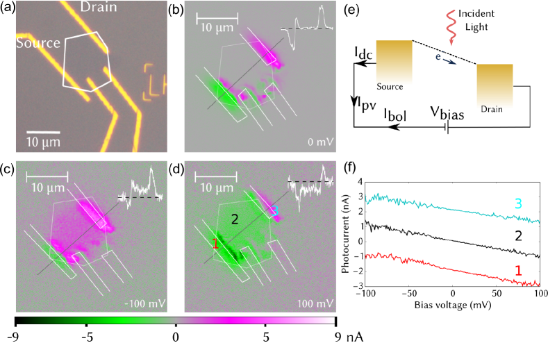
A schematic of the setup used is shown in Figure 1. Light is modulated using an acousto-optic modulator (AOM) at frequencies from 1 kHz up to 100 kHz. As a function of the applied DC gate and bias (source–drain) voltage, the current induced across the source is detected at the light modulation frequency using a lock-in amplifier. The in-phase component of the AC current flowing in the direction of the DC current has been taken to be positive (Figure 1). The far field regime results in a diffraction limited spot size of 1 m in contrast with a higher resolution of 250 nm using a near-field scanning optical microscope (NSOM).
Figure 2 shows the near field SPCM measurements performed on D1. In these measurements, we observe a non-zero background current that is measured when the light is incident on the oxide away from the graphene flake. This has previously been attributed to the light induced photovoltage Freitag et al. (2013) produced at the silicon-silicon dioxide interface which gates the graphene at the modulation frequency and results in a finite measured photocurrent even when the laser is not falling directly on the graphene flake. We compensate for this by subtracting out a constant value from the photocurrent maps so as to make the average background value zero. Strong localized photocurrent is produced near all the electrodes with a large magnitude near the source and drain and a much smaller magnitude near the floating electrodes. We attribute this to the drift currents produced by built–in electric field at the metal–graphene interface because of the difference in work functions. These features have been analyzed in detail in previous work. Park et al. (2009) Thermoelectric contributions, which may also play a role, can be distinguished from photovoltaic contributions by changing the polarization of light. Echtermeyer et al. (2014)
Furthermore, after correcting for the background, at zero bias, there is no current being produced in the graphene region far from the electrodes, but at high biases, there is uniform photocurrent generation throughout graphene. Photocurrent due to the photovoltaic effect and the tilting of the bands is expected to be in the direction of DC current (Figure 2(e)). The observed direction of current is opposite this and therefore it cannot be attributed to the photovoltaic effect. This is instead due to the bolometric effect in which the laser induced heating of graphene causes the resistance to increase, which, in turn causes the photocurrent to flow in a direction opposite to the DC current flowing through the device.
We observe that the data gets noisier at large bias voltages. This is evident in Figure 2 where it can be seen that the background in the photocurrent maps at -100 mV and +100 mV is noisier. Similar results have also been reported in other scanning photocurrent studies but this has not been examined in detail; for example, with MoS2. Wu et al. (2013) This noise is not related to the measurement circuit but is intrinsic to the system. It is absent at zero bias and is seen to scale with the bias voltage. Most previous SPCM measurements on graphene have been done at zero bias where this noise is not visible.
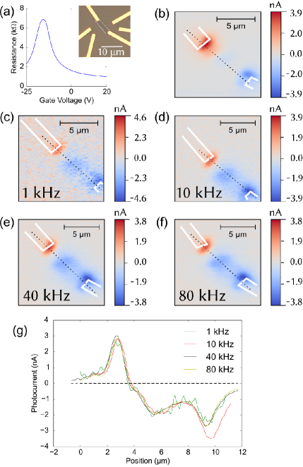
In order to understand the origin and frequency dependence of the noise, we have measured photocurrent maps at different light modulation frequencies. These measurements were done on D2 in a far field system. Our results are summarized in Figure 3 which shows SPCM measurements at a bias of 80 mV and gate voltage of 0 V at modulation frequencies of 1, 10, 40 and 80 kHz. We can observe a strong dependence of the noise on the frequency, with the data noisier at lower frequencies.
We have also varied the bias voltages and frequency while keeping the laser at one point. The results for device D1 in which the bias voltage is scanned from -100 mV to +100 mV are shown in Figure 2(f) after compensating for the background. It can be seen that in the center of the graphene flake, there is no photocurrent but as the bias voltage is increased, the magnitude of the photocurrent increases linearly. The negative slope is indicative of the bolometric effect. In the bolometric effect, a change in temperature causes a change in the conductance which in turn leads to an AC current . For graphene close to room temperature, , Freitag et al. (2013) we get a negative current.
An average laser power of 40 W has been used for device D2. Using this value, we can estimate the change in temperature of graphene using Fourier’s law. Assuming the heat spreads radially around the light spot, we can estimate the temperature increase Balandin et al. (2008) as mK where is the thickness of monolayer graphene, is the incident optical power, is the fraction of power absorbed by the graphene sheet and is the in-plane thermal conductivity for supported graphene. Pop et al. (2012) We have also solved the classical heat equation in two dimensions analytically and using the finite element method (details in supplementary information sup ) and obtain a temperature increase of 800 and 200 mK respectively. The change in conductance at room temperature, as measured in Freitag et al. (2013) is approximately nS/K. Using a temperature increase of 500 mK, we get a conductance change of nS. The corresponding experimental value is 10 nS for device D1 and 20 nS for device D2.
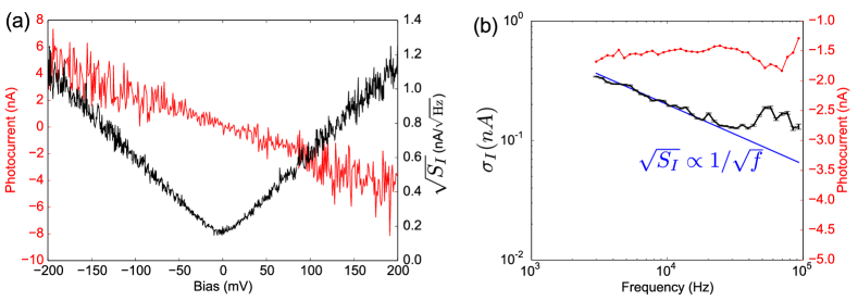
The photocurrent as a function of bias voltage and frequency at the center of the device D2 are shown in Figure 4. The difference of the average value of the fluctuating in-phase component in the center of the graphene flake and the background (Si/SiO2) gives us the change in photocurrent as a function of frequency. We have observed changes in the photocurrent maps between scans with the same parameters, such as forward and backward scans done with the near field (see also Figure 3(g)) and the changes shown in Figure 4(b) of the order of 600 pA are not significant. The bolometric response arises due to a local increase in temperature. The net temperature rise is due to a balance between escape of heat due to large thermal conduction, and absorption due to finite specific heat. We expect a change Richards (1994) in the current at time scales of where the the area of graphene and the thermal diffusivity m2/s (: thermal conductivity, : density, : specific heat). This evaluates to MHz.
We have also studied the characteristics of the noise by measuring its dependence on frequency and bias voltage. Photocurrent measurements at different modulation frequencies in device D2 (Figure 3(c)-(f)) indicate that the noise reduces as the frequency is increased. To calculate the current spectral density , we sweep the light modulation frequency from 3 kHz to 100 kHz and at each frequency, the R component of the lock-in amplifier is sampled and recorded as a function of time. The histogram of the R values at each frequency fits well to a Gaussian distribution and its width is a measure of the temporal fluctuation in photocurrent. We have called this quantity the current fluctuation (shown in Figure 4(b)). This is related to the root of the current spectral density by a factor equal to the square root of the equivalent noise bandwidth () as . We carry out this measurement with the laser spot positioned in the centre of graphene to quantify the noise in the photocurrent. This is plotted in Figure 4(b) and is seen to be in good agreement with a , or equivalently dependence as seen in other graphene devices. Balandin (2013) We can further quantify the noise Liang et al. (2009); Vandamme (2011) using Figure 4 as and obtain . The noise normalized to frequency and area, is . Hooge’s parameterHooge (1969, 1976); Vandamme (2013) where is the total number of charge carriers is .
We have also studied the dependence of the noise on the bias and Figure 4(a) shows that the scaling of the noise on bias is in accordance with Hooge’s empirical law, with the spectral density . The dependence of the photocurrent on the optical power (supplementary information sup section V) shows that the signal to noise ratio improves with increasing laser power. The photocurrent scales with both the optical power and bias, and the noise scales with the bias voltage, indicating that at low optical powers, the bolometric signal will not be visible. Furthermore, the flicker noise will also contribute to the non-zero background as any frequency–dependent AC components of the noise will be picked up by the lock-in amplifier and will contribute to the detected photocurrent. The current spectral density of the non-zero background current measured when the laser is positioned on the silicon dioxide substrate shows a 1/f trend identical to the one shown in Figure 4(b). Increasing the time constant of the lock-in amplifier will reduce the noise bandwidth.
There have been proposals of using graphene as a photodetector using the bolometric effect Freitag et al. (2013) which has the advantage of broadband detection. Muraviev et al. (2013) We have shown that there are noise fluctuations in the photocurrent signal that scale with frequency as 1/f. The bolometric effect, therefore, is accompanied by flicker noise which limits the minimum detectable optical power incident on graphene. We have estimated the noise equivalent power (NEP) of the graphene bolometric detector in the flicker noise regime as W Hz-1/2 valid for the operating frequency . Typical values of NEP for commercial detectors are in the range Agrawal (1997) of 1 – 10 pW Hz-1/2. Flicker noise in graphene arises from the fluctuation in the number of charge carriers and their mobility. Techniques to reduce it such as electron irradiation Zahid Hossain et al. (2013); Liu et al. (2009, 2012); Pal and Ghosh (2009a, b) can be explored in this context. In addition, the high NEP in graphene is also due to the low sensitivity arising in part because of the weak dependence of the graphene resistance with temperature. Koppens et al. (2014)
In conclusion, we have studied the photoresponse of biased graphene and observed that the bolometric effect dominates the photoresponse. The bolometric effect is evident only at non-zero bias voltages and scales linearly with the bias voltage. It is accompanied by flicker noise which increases quadratically with the bias voltage and reduces the signal to noise ratio in graphene photodetectors. We have shown that an optical power of 40 W which corresponds to a temperature increase of 500 mK is sufficient to resolve the bolometric contribution at bias voltages of 100 mV.
The authors thank Ravitej Uppu and N Sreeman Kumar from the Nano Optics and Mesoscopic Optics Laboratory, DNAP, TIFR for their assistance in fabrication of NSOM tips. This work was supported by the Swarnajayanti Fellowship from the Department of Science and Technology and the Department of Atomic Energy of the Government of India.
References
- Novoselov et al. (2004) K. S. Novoselov, A. K. Geim, S. V. Morozov, D. Jiang, Y. Zhang, S. V. Dubonos, I. V. Grigorieva, and A. A. Firsov, Science 306, 666 (2004).
- Xia et al. (2009a) F. Xia, T. Mueller, Y.-m. Lin, A. Valdes-Garcia, and P. Avouris, Nat Nano 4, 839 (2009a).
- Liu et al. (2014) N. Liu, H. Tian, G. Schwartz, J. B.-H. Tok, T.-L. Ren, and Z. Bao, Nano Letters 14, 3702 (2014).
- Sun and Chang (2014) Z. Sun and H. Chang, ACS Nano 8, 4133 (2014).
- H. et al. (2008) L. J. H., K. Balasubramanian, R. T. Weitz, M. Burghard, and K. Kern, Nat Nano 3, 486 (2008).
- Park et al. (2009) J. Park, Y. H. Ahn, and C. Ruiz-Vargas, Nano Letters 9, 1742 (2009).
- Xia et al. (2009b) F. Xia, T. Mueller, R. Golizadeh-Mojarad, M. Freitag, Y.-m. Lin, J. Tsang, V. Perebeinos, and P. Avouris, Nano Letters 9, 1039 (2009b).
- Mueller et al. (2009) T. Mueller, F. Xia, M. Freitag, J. Tsang, and P. Avouris, Phys. Rev. B 79, 245430 (2009).
- Xu et al. (2010) X. Xu, N. M. Gabor, J. S. Alden, A. M. van der Zande, and P. L. McEuen, Nano Letters 10, 562 (2010).
- Ulrich Stützel et al. (2013) E. Ulrich Stützel, T. Dufaux, A. Sagar, S. Rauschenbach, K. Balasubramanian, M. Burghard, and K. Kern, Applied Physics Letters 102, 043106 (2013).
- Freitag et al. (2013) M. Freitag, T. Low, F. Xia, and P. Avouris, Nat Photon 7, 53 (2013).
- Tsen et al. (2008) A. W. Tsen, L. A. K. Donev, H. Kurt, L. H. Herman, and J. Park, Nature Nanotech 4, 108 (2008).
- Low et al. (2014) T. Low, M. Engel, M. Steiner, and P. Avouris, Phys. Rev. B 90, 081408 (2014).
- (14) See supplemental material for instrumentation details, Raman spectra of graphene, dependence of photocurrent on laser power and estimate of temperature increase.
- Echtermeyer et al. (2014) T. J. Echtermeyer, P. S. Nene, M. Trushin, R. V. Gorbachev, A. L. Eiden, S. Milana, Z. Sun, J. Schliemann, E. Lidorikis, K. S. Novoselov, and A. C. Ferrari, Nano Letters 14, 3733 (2014).
- Wu et al. (2013) C.-C. Wu, D. Jariwala, V. K. Sangwan, T. J. Marks, M. C. Hersam, and L. J. Lauhon, The Journal of Physical Chemistry Letters 4, 2508 (2013).
- Balandin et al. (2008) A. A. Balandin, S. Ghosh, W. Bao, I. Calizo, D. Teweldebrhan, F. Miao, and C. N. Lau, Nano Letters 8, 902 (2008).
- Pop et al. (2012) E. Pop, V. Varshney, and A. K. Roy, MRS Bulletin 37, 1273 (2012).
- Richards (1994) P. L. Richards, Journal of Applied Physics 76, 1 (1994).
- Balandin (2013) A. A. Balandin, Nature Nanotech 8, 549 (2013).
- Liang et al. (2009) C. Liang, G. Leroy, J. Gest, L. Vandamme, and J.-L. Wojkiewicz, Synthetic Metals 159, 1 (2009).
- Vandamme (2011) L. Vandamme, Fluctuation and Noise Letters 10, 467 (2011).
- Hooge (1969) F. Hooge, Physics Letters A 29, 139 (1969).
- Hooge (1976) F. Hooge, Physica B+C 83, 14 (1976).
- Vandamme (2013) L. Vandamme, in Noise and Fluctuations (ICNF), 2013 22nd International Conference on (2013) pp. 1–6.
- Muraviev et al. (2013) A. V. Muraviev, S. L. Rumyantsev, G. Liu, A. A. Balandin, W. Knap, and M. S. Shur, Applied Physics Letters 103, 181114 (2013).
- Agrawal (1997) G. Agrawal, Fiber-Optic Communication Systems, Wiley Series in Microwave and Optical Engineering (Wiley, 1997).
- Zahid Hossain et al. (2013) M. Zahid Hossain, S. Rumyantsev, M. S. Shur, and A. A. Balandin, Applied Physics Letters 102, 153512 (2013).
- Liu et al. (2009) G. Liu, W. Stillman, S. Rumyantsev, Q. Shao, M. Shur, and A. A. Balandin, Applied Physics Letters 95, 033103 (2009).
- Liu et al. (2012) G. Liu, S. Rumyantsev, M. Shur, and A. A. Balandin, Applied Physics Letters 100, 033103 (2012).
- Pal and Ghosh (2009a) A. N. Pal and A. Ghosh, Applied Physics Letters 95, 082105 (2009a).
- Pal and Ghosh (2009b) A. N. Pal and A. Ghosh, Phys. Rev. Lett. 102, 126805 (2009b).
- Koppens et al. (2014) F. H. L. Koppens, T. Mueller, P. Avouris, A. C. Ferrari, M. S. Vitiello, and M. Polini, Nat Nano 9, 780 (2014).