Transport, Aharonov-Bohm, and Topological Effects in Graphene Molecular Junctions and Graphene Nanorings
Abstract
The unique ultra-relativistic, massless, nature of electron states in two-dimensional extended graphene sheets, brought about by the honeycomb lattice arrangement of carbon atoms in two-dimensions, provides ingress to explorations of fundamental physical phenomena in graphene nanostructures. Here we explore the emergence of new behavior of electrons in atomically precise segmented graphene nanoribbons (GNRs) and graphene rings with the use of tight-binding calculations, non-equilibrium Green’s function transport theory, and a newly developed Dirac continuum model that absorbs the valence-to-conductance energy gaps as position-dependent masses, including topological-in-origin mass-barriers at the contacts between segments. Through transport investigations in variable-width segmented GNRs with armchair, zigzag, and mixed edge terminations we uncover development of new Fabry-Pérot-like interference patterns in segmented GNRs, a crossover from the ultra-relativistic massless regime, characteristic of extended graphene systems, to a massive relativistic behavior in narrow armchair GNRs, and the emergence of nonrelativistic behavior in zigzag-terminated GNRs. Evaluation of the electronic states in a polygonal graphene nanoring under the influence of an applied magnetic field in the Aharonov-Bohm regime, and their analysis with the use of a relativistic quantum-field theoretical model, unveils development of a topological-in-origin zero-energy soliton state and charge fractionization. These results provide a unifying framework for analysis of electronic states, coherent transport phenomena, and the interpretation of forthcoming experiments in segmented graphene nanoribbons and polygonal rings.
1 Introduction
In the last three decades transport through molecular junctions 1, 2, 3, 4, 5, 6 has attracted much attention because of fundamental aspects of the processes involved, as well as of potential practical prospects. In particular, studies in this direction have intensified since the discovery of new forms of carbon allotropes, starting with the fullerenes 7 and carbon nanotubes 8 (CNTs) in the 1980s and 1990s respectively, and the isolation of graphene 9 in 2004. The above carbon allotropes differ in shape (curvature), topology, and dimensionality, with the fullerenes being zero-dimensional (0D) with spherical or prolate shape, the CNTs being one-dimensional (1D) cylinders, and graphene being a two-dimensional (2D) plane (or 1D planar ribbons 10, 11, 12, 13). In the fullerenes the carbon-atom network is made of (non-adjacent) hexagons and pentagons, whereas the CNTs and graphene are entirely hexagonal lattices (curved in CNTs) described in terms of a unit cell with a two-atom basis with the two carbon atoms occupying two sublattices ( and , also mapped into the up and down pseudospin states 14). In the absence of defects, in-plane () bonding occurs through hybrid orbitals and out-of-plane bonding () involves the orbital; in the following only the physics of -states is considered.
The hexagonal network topology of graphene gives rise to relativistic behavior of the low-energy excitations which is captured by the ultra-relativistic massless Dirac-Weyl (DW) equation, with the Fermi velocity of graphene () replacing the velocity of light. 14 Among the many manifestations of the relativistic behavior in graphene is the Klein paradox, that is “… unimpeded penetration of relativistic particles through high and wide potential barriers – is one of the most exotic and counterintuitive consequences of quantum electrodynamics.”15 The surprising relativistic behavior in graphene has indeed been recognized in the 2010 Nobel award in physics to A. Geim and K. Novosolev.
Another carbon-based system that was the subject of an earlier (2000) chemistry Nobel award (to A.J. Heeger, A.G. MacDiarmid, and H. Shirakawa) is conductive polymers, with polyacetelyne (PAC) being a representative example. 16 PAC is a 1D chain of carbon atoms forming a conjugated polymer with hybridization that leads to one unpaired electron per carbon atom (half-filled -band) as in graphene. Linearizing the spectrum of this 1D equally-spaced carbon chain at the Fermi level (that is at the Dirac points, i.e., the zero-energy points of the energy vs momentum dispersion relation) results in a 1D massless Dirac-equation description of the low energy excitations of the system. 17, 18
However, the equally-spaced 1D system is unstable and consequently it distorts (structurally) spontaneously (Peierls distortion 19) yielding a modulation (alternation) of the spacing between successive sites that results in dimerization of successive atoms along the chain and the opening of a gap in the electronic spectrum. This dimerization can occur in two energetically degenerate, but spatially distinct, patterns, termed as equivalent domain structures. Either of these domains is a realization of the 1D Dirac equation with a constant mass term, . Disruption of the dimerization pattern (e.g., by transforming from one domain to another along the chain) creates a domain wall which can be described in the 1D Dirac formulation through the use of a position-dependent mass term of alternating sign (with the spatial mass-profile connecting with ). The solution of this generalized 1D Dirac equation is a soliton characterized by having zero energy and by being localized at the domain wall. In this paper, the Dirac equation with position-dependent mass will be used in investigations of the electronic structure, transport, and magnetic-field-induced phenomena (Aharonov-Bohm) in graphene nanostructures such as nanoribbon junctions and rings. 20, 21, 22
From the above we conclude that in the two extreme size-domains, that is a 2D infinite graphene sheet and a 1D carbon chain (PAC), the systems exhibit behavior that is relativistic in nature. In an attempt to bridge between these two size-domains, we briefly discuss in the following systems of successively larger width, starting from the polyacene (a quasi-1D chain of fused benzene rings) which may be regarded as the narrowest graphene nanoribbon (GNR) with zigzag edge terminations.
Polyacene was investigated 23 first in 1983. It was found that, as in graphene and PAC (without distortion), the valence and conduction bands of undistorted polyacene touch at the edge of the Brillouin zone. However, unlike 2D graphene and PAC, the dispersion relation about the touching point is quadratic, conferring a non-relativistic (Schrödinger equation) character. We show in this paper that this surprising finding persists for sufficiently narrow GNRs with zigzag termination (zGNRs). However, narrow armchair-terminated GNRs (aGNRs) are found here to maintain relativistic behavior, with metallic ones being massless and semiconducting ones being massive (both classes obeying the Einstein energy relation).
It this paper, we discuss mainly manifestations of relativistic and/or nonrelativistic quantum behavior explored through theoretical considerations of transport measurements in segmented graphene nanoribbons of variable width, and spectral and topological effects in graphene nanorings in the presence of magnetic fields.
Transport through narrow graphene channels particularly bottom-up fabricated and atomically-precise graphene nanoribbons 24, 25, 26, 27, 28, 29, 30, 31 is expected to offer ingress to unique behavior of Dirac electrons in graphene nanostructures. In particular, the wave nature of elementary particles (e.g., electrons and photons) is commonly manifested and demonstrated in transport processes. Because of an exceptionally high electron mobility and a long mean-free path, it has been anticipated that graphene 14 devices hold the promise for the realization, measurement, and possible utilization of fundamental aspects of coherent and ballistic transport behavior, which to date have been observed, with varying degrees of success, mainly at semiconductor interfaces 32, 33, quantum point contacts 34, metallic wires 35, and carbon nanotubes 36.
Another manifestation of coherent ballistic transport are interference phenomena, reflecting the wave nature of the transporting physical object, and associated most often with optical (electromagnetic waves, photons) systems or with analogies to such systems (that is, the behavior of massless particles, as in graphene sheets). Measurements of interference patterns are commonly made with the use of interferometers, most familiar among them the multi-pass optical Fabry-Pérot (OFP) interferometer 37, 38. The advent of 2D forms of carbon allotropes has motivated the study of optical-like interference phenomena associated with relativistic massless electrons, as in the case of metallic carbon nanotubes 36 and graphene 2D - junctions 39. (We note that the hallmark of the OFP is that the energy separation between successive maxima of the interference pattern varies as the inverse of the cavity length .)
For GNRs with segments of different widths, our investigations reveal diverse Fabry-Pérot transport modes beyond the OFP case, with conductance quantization steps (, with ) found only for uniform GNRs. In particular, three distinct categories of Fabry-Pérot interference patterns are identified:
-
1.
FP-A: An optical FP pattern corresponding to massless graphene electrons exhibiting equal spacing between neighboring peaks. This pattern is associated with metallic armchair nanoribbon central segments. This category is subdivided further to FP-A1 and FP-A2 depending on whether a valence-to-conduction gap is absent (FP-A1, associated with metallic armchair leads), or present (FP-A2, corresponding to semiconducting armchair leads).
-
2.
FP-B: A massive relativistic FP pattern exhibiting a shift in the conduction onset due to the valence-to-conduction gap and unequal peak spacings. This pattern is associated with semiconducting armchair nanoribbon central segments, irrespective of whether the leads are metallic armchair, semiconducting armchair, or zigzag.
-
3.
FP-C: A massive non-relativistic FP pattern with peak spacings, but with a vanishing valence-to-conduction gap, being the length of the central segment. This pattern is the one expected for usual semiconductors described by the (nonrelativistic) Schrödinger equation, and it is associated with zigzag nanoribbon central segments, irrespective of whether zigzag or metallic armchair leads are used.
We report in this paper on the unique apects of transport through segmented GNRs obtained from tight-binding non-equilibrium Green’s function 40, 41 (TB-NEGF) calculations in conjunction with an analysis based on a one-dimensional (1D) relativistic Dirac continuum model. This continuum model goes beyond the physics of the massless Dirac-Weyl (DW) electron, familiar from two-dimensional (2D) honeycomb carbon sheets 14, and it is referred to by us as the Dirac-Fabry-Pérot (DFP) theory (see below for the choice of name). In particular, it is shown that the valence-to-conduction energy gap in armchair GNR (aGNR) segments, as well as the barriers at the interfaces between nanoribbon segments, can be incorporated in an effective position-dependent mass term in the Dirac hamiltonian; the transport solutions associated with this hamiltonian exhibit conductance patterns comparable to those obtained from the microscopic NEGF calculations. For zigzag graphene nanoribbon (zGNR) segments, the valence-to-conduction energy gap vanishes, and the mass term is consonant with excitations corresponding to massive nonrelativistic Schrödinger-type carriers. The faithful reproduction of these unique TB-NEGF conductance patterns by the DFP theory, including mixed armchair-zigzag configurations (where the carriers transit from a relativistic to a nonrelativistic regime), provides a unifying framework for analysis of coherent transport phenomena and for interpretation of experiments targeting fundamental understanding of transport in GNRs and the future development of graphene nanoelectronics.
To demonstrate the aforementioned soliton formation due to structural topological effects (discussed by us above in the context of polyacetylene), we explore with numerical tight-binding calculations and a Dirac-Kronig-Penney (DKP) approach, soliton formation and charge fractionization in graphene rhombic rings; this DKP approach is based on a generalized Dirac equation with alternating-sign position-dependent masses.
Before leaving the Introduction, we mention that, due to their importance as fundamental phenomena, Aharonov-Bohm-type effects in graphene-nanoribbons systems have attracted (in addition to Refs. 20, 21, 22) considerable theoretical attention. 4, 42, 43, 44, 45, 46, 47 These latter theoretical papers, however, based their analysis exclusively on tight-binding and/or DFT calculations4, 42, 44, 46, 47, or they used in addition a two-dimensional Dirac equation with infinite-mass boundary conditions.43, 45 Transcending the level of current understanding which explores direct similaritiess with the Aharonov-Bohm physics in semiconductor and metallic mesoscopic rings, our work here analyzes the TB results in conjunction with a continuum 1D generalized Dirac equation (that incorporates a position-dependent mass term), and thus it enables investigations of until-now unexplored topological aspects and relativistic quantum-field analogies of the AB effect in graphene nanosystems.
Furthermore we note that oscillations in the conductance of graphene nanoribbons in the presence of magnetic barriers were found in a theoretical study 48 (using exclusively a TB-NEGF approach), as well as in an experimental investigation of high quality bilayer nanoribbons, 49 and they were attributed to Fabry-Pérot-type interference. In the absence of a continuum Dirac analysis, the precise relation of such oscillatory patterns to our Fabry-Pérot theory (based on the incorporation of a position-dependent mass term in the Dirac equation at zero magnetic field) warrants further investigation.
Finally, gap engineering in graphene ribbons under strong external fields was studied in Ref. 50. We stress again that one of the main results in this paper is the appearance of “forbidden” solitonic states inside the energy gap in the context of the low-magnetic-field Aharonov-Bohm spectra of graphene nanorings; see the part titled “Aharonov-Bohm spectra of rhombic graphene rings” in the Results section.
2 Methods
2.1 Dirac-Fabry-Pérot model
The energy of a fermion (with one-dimensional momentum ) is given by the Einstein relativistic relation , where is the rest mass and is the Fermi velocity of graphene. In a gapped uniform graphene nanoribbon, the mass parameter is related to the particle-hole energy gap, , as . Following the relativisitic quantum-field Lagrangian formalism, the mass is replaced by a position-dependent scalar Higgs field , to which the relativistic fermionic field couples through the Yukawa Lagrangian 21 ( being a Pauli matrix). For (constant) , and the massive fermion Dirac theory is recovered. The Dirac equation is generalized as (here we do not consider applied electric or magnetic fields)
| (1) |
In one dimension, the fermion field is a two-component spinor ; and stand, respectively, for the upper and lower component and and can be any two of the three Pauli matrices. Note that the Higgs field enters in the last term of Eq. (1). in the first term is the usual electrostatic potential, which is inoperative due to the Klein phenomenon and thus is set to zero for the case of the armchair nanoribbons (where the excitations are relativistic). The generalized Dirac Eq. (1) is used in the construction of the transfer matrices of the Dirac-Fabry-Pérot model described below.
The building block of the DFP model is a 22 wave-function matrix formed by the components of two independent spinor solutions (at a point ) of the onedimensional, first-order generalized Dirac equation [see Eq. (3) in the main paper]. plays 51 the role of the Wronskian matrix used in the second-order nonrelativistic Kronig-Penney model. Following Ref. 51 and generalizing to regions, we use the simple form of in the Dirac representation (, ), namely
| (2) |
where
| (3) |
The transfer matrix for a given region (extending between two matching points and specifying the potential steps ) is the product ; this latter matrix depends only on the width of the region, and not separately on or .
The transfer matrix corresponding to a series of regions can be formed 21 as the product
| (4) |
where is the width of the th region [with ]. The transfer matrix associated with the transmission of a free fermion of mass (incoming from the right) through the multiple mass barriers is the product
| (5) |
with , ; for armchair leads , while for zigzag leads . Naturally, in the case of metallic armchair leads, , since .
Then the transmission coefficient is
| (6) |
while the reflection coefficient is given by
| (7) |
At zero temperature, the conductance is given by ;
is the transmission coefficient in Eq. (6).
2.2 Dirac-Kronig-Penney superlatice model
The transfer matrix corresponding to either half of the rhombus can be formed 21 as the product
| (8) |
with being the length of half of the perimeter of the rhombus; , with and . The transfer matrix associated with the complete unit cell (encircling the rhombic ring) is the product
| (9) |
Following Refs. 21, 52, we consider the superlattice generated from the virtual periodic translation of the unit cell as a result of the application of a magnetic field perpendicular to the ring. Then the Aharonov-Bohm energy spectra are given as solutions of the dispersion relation
| (10) |
where we have explicitly denoted the dependence of the r.h.s. on the energy ; for a rhombus with type-I corners and for a rhombus with type-II corners.
The energy spectra and single-particle densities do not depend on a specific representation. However, the wave functions (upper and lower spinor components of the fermionic field ) do depend on the representation used. To transform the initial DKP wave functions to the (, ) representation, which corresponds to the natural separation of the tight-binding amplitudes into the and sublattices, we apply successively the unitary transformations and .
2.3 TB-NEGF formalism
To describe the properties of graphene nanostructures in the tight-binding approximation, we use the hamiltonian
| (11) |
with indicating summation over the nearest-neighbor sites . eV is the hopping parameter of two-dimensional graphene.
To calculate the TB-NEGF transmission coefficients, the Hamiltonian (11) is employed in conjunction with the well known transport formalism which is based on the nonequilibrium Green’s functions 40, 41.
According to the Landauer theory, the linear conductance is , where the transmission coefficient is calculated as . The Green’s function is given by
| (12) |
with being the Hamiltonian of the isolated device (junction without the leads). The self-energies are given by , where the hopping matrices describe the left (right) device-to-lead coupling, and is the Hamiltonian of the semi-infinite left (right) lead. The broadening matrices are given by .
3 Results
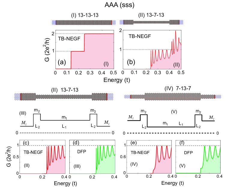
3.1 Segmented Armchair GNRs: All-semiconducting
Our results for a 3-segment (, where is the lead width and is the width of the central segment) all-semiconducting aGNR, AAA (sss), are portrayed in Fig. 1 [see schematic lattice diagrams in Figs. 1(I) and 1(II)]. A uniform semiconducting armchair GNR [see Fig. 1(I)] exhibits ballistic quantized-conductance steps [see Fig. 1(a)]. In contrast, conductance quantization is absent for a nonuniform 3-segment () aGNR; see Figs. 1(b) 1(d). Here oscillations appear instead of quantized steps. The first oscillation appears at an energy [Fig. 1(b)], which reflects the intrinsic gap of the semiconducting central segment belonging to the class II of aGNRs, specified 10, 13, 22 by a width , . We recall that as a function of their width, , the armchair graphene nanoribbons fall into three classes: (I) (semiconducting, ), (II) (semiconducting, ), and (III) (metallic, ), .
That the leads are semiconducting does not have any major effect. This is due to the fact that , and as a result the energy gap of the central segment is larger than the energy gap of the semiconducting leads [see schematic in Fig. 1(III)]. In the opposite case (central segment wider than the leads), the energy gap of the semiconducting leads would have determined the onset of the conductance oscillations.
The armchair GNR case with interchanged widths (i.e., instead of ) is portrayed in Figs. 1(e) 1(f). In this case the energy gap of the semiconducting leads (being the largest) determines the onset of the conductance oscillations. It is a testimonial of the consistency of our DFP method that it can reproduce [see Fig. 1(d) and Fig. 1(f)] both the and TB-NEGF conductances; this is achieved with very similar sets of parameters taking into consideration the central-segment-leads interchange. We note that the larger spacing between peaks (and also the smaller number of peaks) in the case is due to the smaller mass of the central segment ( instead of ).
Further insight can be gained by an analysis of the discrete energies associated with the humps of the conductance oscillations in Fig. 1(c) and the resonant spikes in Fig. 1(e). Indeed a simplified approximation for the electron confinement in the continuum model consists in considering the graphene electrons as being trapped within a 1D infinite-mass square well (IMSW) of length (the mass terms are infinite outside the interval and the coupling to the leads vanishes). The discrete spectrum of the electrons in this case is given 53 by
| (13) |
where the wave numbers are solutions of the transcendental equation
| (14) |
When [massless Dirac-Weyl (DW) electrons], one finds for the spectrum of the IMSW model:
| (15) |
with .
| (16) |
which is twice the energy
| (17) |
of the lowest state.
As is well known, a constant energy separation of the intensity peaks, inversely proportional to the length of the resonating cavity [here , see Eqs. (16) and (17) above] is the hallmark of the optical Fabry-Pérot, reflecting the linear energy dispersion of the photon in optics 38 or a massless DW electron in graphene structures.36 Most revealing is the energy offset away form zero of the first conductance peak, which equals exactly one-half of the constant energy separation between the peaks. In one-dimension, this is the hallmark of a massless fermion subject to an infinite-mass-barrier confinement 53. Naturally, in the case of a semiconducting segment (see below), this equidistant behavior and -offset of the conductance peaks do not apply; this case is accounted for by the Dirac-Fabry-Pérot model presented in Methods, and it is more general than the optical Fabry-Pérot theory associated with a photonic cavity. 38
In the nonrelativistic limit, i.e., when , one gets
| (18) |
which yields the well known relations and
| (19) |
For a massive relativistic electron, as is the case with the semiconducting aGNRs in this paper, one has to numerically solve Eq. (14) and then substitute the corresponding value of in Einstein’s energy relation given by Eq. (13).
From an inspection of Fig. 1, one can conclude that the physics associated with the all-semiconducting AAA junction is that of multiple reflections of a massive relativistic Dirac fermion bouncing back and forth from the edges of a “quantum box” created by a double-mass barrier [see the schematic of the double-mass barrier in Figs. 1(III) and 1(V)]. In particular, to a good approximation the energies of the conductance oscillation peaks are given by the IMSW Eq. (14) with () or (). In this respect, the separation energy between successive peaks in Figs. 1(b), 1(c), 1(e), and 1(f) is not a constant, unlike the case of an all-metallic junction 36 (or a photonic cavity 38).
The conductance patterns in Figs. 1(d) and 1(f) correspond to the category FP-B (see the introductory section). These patterns cannot be accounted for by the optical Fabry-Pérot theory, but they are well reproduced by the generalized Dirac-Fabry-Pérot model introduced by us in the Methods section.
![[Uncaptioned image]](/html/1502.04746/assets/x2.png)
(Right) H-passivation effects in the conductance of a 3-segment armchair nanoribbon with a metallic () central constriction and semiconducting leads (); see schematic lattice diagram in (III). Note that the nearest-neighbor C-C bonds at the armchair edges (thick red and blue lines) have hopping parameters . (IV) Schematics of the position-dependent mass field used in the DFP modeling. (e) TB-NEGF conductance as a function of the Fermi energy. (f) DFP conductance reproducing the TB-NEGF result in (e). The mass parameters used in the DFP reproduction were , , , . The mass of the electrons in the leads was . (g)-(h) The total DOS of the junction and the density of states in the isolated leads, respectively, according to the TB-NEGF calculations. The arrows indicate the onset of the electronic bands in the leads; note the shifts from to and from to for the onsets of the first and second bands, respectively, compared to the case with in (d). Compared to left part of Fig. 2, the subtle modifications of mass parameters brought about by having result in having six sharp electronic states [see (g)] below the onset (at ) of the first band in the leads [see (h)], which consequently do not generate any conductance resonances [see (e) and (f)]. In addition, within the energy range ( to ) shown in (e) and (f), there are now only two conducting resonances, instead of three compared to (a) and (b). nm is the graphene lattice constant; eV is the graphene hopping parameter.
3.2 Segmented Armchair GNRs: semiconducting-metallic-semiconducting.
Our results for a 3-segment () semiconducting-metallic-semiconducting aGNR, AAA (sms), are portrayed in Fig. 2 [left, see schematic lattice diagram in Fig. 2(I)]. The first FP oscillation in the TB-NEGF conductance displayed in Fig. 2(a) appears at an energy , which reflects the intrinsic gap of the semiconducting leads (with ). The energy spacing between the peaks in Fig. 2(a) is constant in agreement with the metallic (massless DW electrons) character of the central segment with . The TB-NEGF pattern in Fig. 2(a) corresponds to the Fabry-Pérot category FP-A2. As seen from Fig. 2(b), our generalized Dirac-Fabry-Pérot theory is again capable of faithfully reproducing this behavior.
A deeper understanding of the AAA (sms) case can be gained via an inspection of the density of states (DOS) plotted in Fig. 2(c) for the total segmented aGNR (central segment plus leads) and in Fig. 2(d) for the the isolated leads. In Fig. 2(c), nine equidistant resonance lines are seen. Their energies are close to those resulting from the IMSW Eq. (15) (with , see the caption of Fig. 2) for a massless DW electron. Out of these nine resonances, the first five do not conduct [compare Figs. 2(a) and 2(c)] because their energies are lower than the minimum energy (i.e., ) of the incoming electrons in the leads [see the onset of the first band (marked by an arrow) in the DOS curve displayed in Fig. 2(d)].
3.3 Segmented Armchair GNRs: Effects of hydrogen passivation.
As shown in Refs. 11, 12, a detailed description of hygrogen passivation requires that the hopping parameters for the nearest-neighbor C-C bonds at the armchair edges be given by . Taking this modification into account, our results for a 3-segment semiconducting-metallic-semiconducting aGNR are portrayed in Fig. 2 [right, see schematic lattice diagram in Fig. 2(III)]; this lattice configuration is denoted as ”AAA (sms) H-passivation.” The first FP oscillation in the TB-NEGF conductance displayed in Fig. 2(e) appears at an energy , which reflects the intrinsic gap of the properly passivated semiconducting leads (with ). The energy spacing between the peaks in Fig. 2(e) is slightly away from being constant in agreement with the small mass acquired by the central segment with , due to taking . As seen from Fig. 2(f), our generalized Dirac-Fabry-Pérot theory is again capable of faithfully reproducing this behavior.
A deeper understanding of the AAA (sms)-H-passivation case can be gained via an inspection of the DOS plotted in Fig. 2(g) for the total segmented aGNR (central segment plus leads) and in Fig. 2(h) for the isolated leads. In Fig. 2(g), eight (almost, but not exactly, equidistant) resonance lines are seen. Their energies are close to those resulting from the IMSW Eq. (14) (with and ; see the caption of Fig. 2) for a Dirac electron with a small mass. Out of these eight resonances, the first six do not conduct [compare Figs. 2(e) and 2(g)] because their energies are lower than the minimum energy (i.e., ) of the incoming electrons in the leads [see the onset of the first band (marked by an arrow) in the DOS curve displayed in Fig. 2(h)]. From the above we conclude that hydrogen passivation of the aGNR resulted in a small shift of the location of the states, and opening of a small gap for the central metallic narrower (with a width of ) segment, but did not modify the conductance record in any qualitative way. Moreover, the passivation effect can be faithfully captured by the Dirac FP model by a small readjustment of the model parameters.
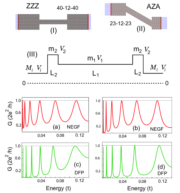
3.4 All-zigzag segmented GNRs.
It is interesting to investigate the sensitivity of the interference features on the edge morphology. We show in this section that the relativistic transport treatment applied to segmented armchaie GNRs does not maintain for the case of a nanoribbon segment with zigzag edge terminations. In fact zigzag GNR (zGNR) segments exhibit properties akin to the well-known transport in usual semiconductors, i.e., their excitations are governed by the nonrelativistic Schrödinger equation.
Before discussing segmented GNRs with zigzag edge terminations, we remark that such GNRs with uniform width exhibit stepwise quantization of the conductance, similar to the case of a uniform armchair-edge-terminated GNR [see Fig. 1(a)].
In Fig. 3(a), we display the conductance in a three-segment junction [see lattice schematic in Fig. 3(I)] when all three segments have zigzag edge terminations (denoted as ZZZ), but the central one is narrower than the lead segments. The main finding is that the central segment behaves again as a resonant cavity that yields an oscillatory conductance pattern where the peak spacings are unequal [Fig. 3(a)]. This feature, which deviates from the optical Fabry-Pérot behavior, appeared also in the DFP patterns for a three-segment armchair junction whose central segment was semiconducting, albeit with a different dependence on [see Figs. 1 and Eq. (14)]. Moreover, from a set of systematic calculations (not shown) employing different lengths and widths, we found that the energy of the resonant levels in zGNR segments varies on the average as , where the integer counts the resonances and indicates the length of the central segment. However, a determining difference with the armchair GNR case in Fig. 1 is the vanishing of the valence-to-conductance gap in the zigzag case of Fig. 3(a). It is well known that the above features are associated with resonant transport of electronic excitations that obey the nonrelativistic second-order Schrödinger equation.
Naturally, one could formulate a continuum transport theory based on transfer matrices (see Methods) that use the 1D Schrödinger equation instead of the generalized Dirac Eq. (1). Such a Schrödinger-equation continuum approach, however, is unable to describe mixed armchair-zigzag interfaces (see below), where the electron transits between two extreme regimes, i.e., an ultrarelativistic (i.e., including the limit of vanishing carrier mass) Dirac regime (armchair segment) and a nonrelativistic Schrödinger regime (zigzag segment). We have thus been led to adopt the same Dirac-type transfer-matrix approach as with the armchair GNRs, but with nonvanishing potentials . This amounts to shifts (in opposite senses) of the energy scales for particle and hole excitations, respectively, and it yields the desired vanishing value for the valence-to-conduction gap of zigzag GNRs.
The calculated DFP conductance that reproduces well the TB-NEGF result for the ZZZ junction [Fig. 3(a)] is displayed in Fig. 3(c); the parameters used in the DFP calculation are given in the caption of Fig. 3. We note that the carrier mass () in the central zigzag segment exhibits an energy dependence. This is similar to a well known effect (due to nonparabolicity in the dispersion) in the transport theory of usual semiconductors 54. We further note that the average mass associated with a zigzag segment is an order of magnitude larger than that found for semiconducting armchair segments of similar width (see caption in Fig. 1), and this yields energy levels close to the nonrelativistic limit [see Eq. (19)]. We note that the FP pattern of the ZZZ junction belongs to the category FP-C.
3.5 Mixed armchair-zigzag-armchair segmented GNRs.
Fig. 3 (right column) presents an example of a mixed armchair-zigzag-armchair (AZA) junction, where the central segment has again zigzag edge terminations [see lattice schematic in Fig. 3(II)]. The corresponding TB-NEGF conductance is displayed in Fig. 3(b). In spite of the different morphology of the edges between the leads (armchair) and the central segment (zigzag), the conductance profile of the AZA junction [Fig. 3(b)] is very similar to that of the ZZZ junction [Fig. 3(a)]. This means that the characteristics of the transport are determined mainly by the central segment, with the left and right leads, whether zigzag or armchair, acting as reservoirs supplying the impinging electrons.
The DFP result reproducing the TB-NEGF conductance is displayed in Fig. 3(d), and the parameters used are given in the caption. We stress that the mixed AZA junction represents a rather unusual physical regime, where an ultrarelativistic Dirac-Weyl massless charge carrier (due to the metallic armchair GNRs in the leads) transits to a nonrelativistic massive Schrödinger electron in the central segment. We note that the FP pattern of the AZA junction belongs to the FP-C caregory.
3.6 Aharonov-Bohm spectra of rhombic graphene rings.
The energy of a particle (with onedimensional momentum ) is given by the Einstein relativistic relation , where is the rest mass. As aforementioned, in armchair graphene ribbons, the mass parameter is related to the particle-hole energy gap, , as . In relativistic quantum field theory, the mass of elementary particles is imparted through interaction with a scalar field known as the Higgs field. Accordingly, the mass is replaced by a position-dependent Higgs field , to which the relativistic fermionic field couples through the Yukawa Lagrangian 55, 56, 21 ( being a Pauli matrix). In the elementary-particles Standard Model, 57 such coupling is responsible for the masses of quarks and leptons. For (constant) , and the massive fermion Dirac theory is recovered.
We exploit the generalized Dirac physics governed by a total Lagrangian density , where the fermionic part is given by
| (20) |
and the scalar-field part has the form
| (21) |
with the potential (second term) assumed to have a double-well form; and are constants.
Henceforth, the Dirac equation (see Methods) is generalized as
| (22) |
In one dimension, the fermion field is a two-component spinor ; and stand, respectively, for the upper and lower component and and can be any two of the three Pauli matrices.
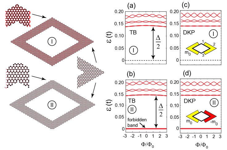
A graphene polygonal ring can be viewed as made of connected graphene-nanoribbon fragments (here we consider aGNRs). The excitations of an infinite aGNR are described by the 1D massive Dirac equation, see Eq. (22) with , , and . The two (in general) unequal hopping parameters and are associated with an effective 1D tight-binding problem) and are given 58 by , and ; is the number of carbon atoms specifying the width of the nanoribbon and eV is the hopping parameter for 2D graphene. The effective 58 TB Hamiltonian of an aGNR has a form similar to that used in trans-polyacetylene (a single chain of carbon atoms). In trans-polyacetylene, the inequality of and (referred to as dimerization) is a consequence of the aforementioned Peierls distortion induced by the electron-phonon coupling. For an armchair graphene ring, this inequality is a topological effect associated with the geometry of the edge and the width of the ribbon. We recall that as a function of their width, , the armchair graphene nanoribbons fall into three classes: (I) (semiconducting, ), (II) (semiconducting, ), and (III) (metallic ), .
We adapt the “crystal” approach 52 to the Aharonov-Bohm (AB) effect, and introduce a virtual Dirac-Kronig-Penney 51 (DKP) relativistic superlattice (see Methods). Charged fermions in a perpendicular magnetic field circulating around the ring behave like electrons in a spatially periodic structure (period ) with the magnetic flux () playing the role of the Bloch wave vector , i.e., [see the cosine term in Eq. (10)].
Naturally, nanorings with arms made of nanoribbon segments belonging to the semiconducting classes may be expected to exhibit a particle-hole gap (particle-antiparticle gap in RQF theory). Indeed this is found for a rhombic armchair graphene ring (AGR) [see gap in Fig. 4(a)] with a width of carbon atoms having type-I corners. Suprisingly, a rhombic armchair graphene nanoring of the same width , but having corners of type-II, demonstrates a different behavior, showing a “forbidden” band (with ) in the middle of the gap region [see Fig. 4(b)].
This behavior of rhombic armchair graphene rings with type-II corners can be explained through analogies with RQF theoretical models, describing single zero-energy fermionic solitons with fractional charge 59, 17 or their modifications when forming soliton/anti-soliton systems. 60, 17 (A solution of the equation of motion corresponding to Eq. (21), is a kink soliton, . The solution of Eq. (22) with is the fermionic soliton.) We model the rhombic ring with the use of a continuous 1D Kronig-Penney 51 model (see Methods) based on the generalized Dirac equation (22), allowing variation of the scalar field along the ring’s arms. We find that the DKP model reproduces [see Fig. 4(d)] the spectrum of the type-II rhombic ring (including the forbidden band) when considering alternating masses associated with each half of the ring [see inset in Fig. 4(d)].
In analogy with the physics of trans-polyacetylene (see remarks in the introductory section), the positive and negative masses correspond to two degenerate domains associated with the two possible dimerization patterns 17, 16 and , which are possible in a single-atom chain. The transition zones between the two domains (here two of the four corners of the rhombic ring) are referred to as the domain walls.
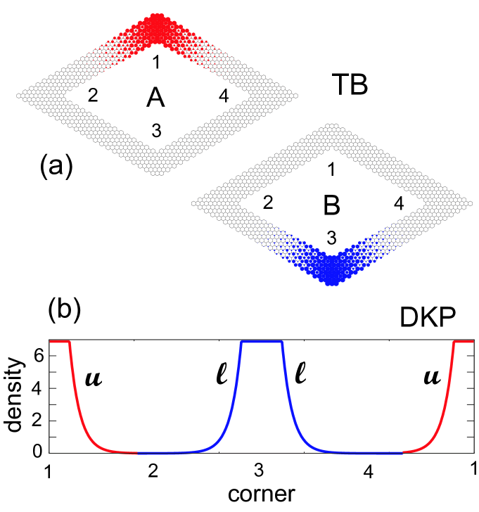
For a single soliton, a (precise) zero-energy fermionic excitation emerges, localized at the domain wall. In the case of soliton-antisoliton pairs, paired energy levels with small positive and negative values appear within the gap. The TB spectrum in Fig. 4(b) exhibits a forbidden band of two paired levels, a property fully reproduced by the DKP model that employs two alternating mass domains [Fig. 4(d). The twofold forbidden band with appears as a straight line due to the very small amplitude oscillations of its two members. nm is the graphene lattice constant and eV is the hopping parameter.
The strong localization of a fraction of a fermion at the domain walls (two of the rhombus’ corners), characteristic of fermionic solitons 17 and of soliton/anti-soliton pairs, 60 is clearly seen in the TB density distributions (modulus of single-particle wave functions) displayed in Fig. 5(a). The TB () sublattice component of the tight-binding wave functions localizes at the odd numbered corners. These alternating localization patterns are faithfully reproduced [see Fig. 5(b)] by the upper, , and lower, , spinor components of the continuum DKP model. The soliton-antisoliton pair in Fig. 5(b) generates an charge fractionization at each of the odd-numbered corners, which is similar to the fractionization familiar from polyacetylene.
The absence of a forbidden band (i.e., solitonic excitations within the gap) in the spectrum of the type-I rhombic nanorings [see Fig. 4(a)] indicates that the corners in this case do not induce an alternation between the two equivalent dimerized domains (represented by in the DKP model). Here the corners do not act as topological domain walls. Nevertheless, direct correspondence between the TB and DKP spectra is achieved here too by using a variable Higgs field defined as with and [see the schematic inset in Fig. 4(c) and the DKP spectrum plotted in the same figure].
4 Discussion
In this paper we focused on manifestations of relativistic and/or nonrelativistic quantum behavior explored through theoretical considerations of transport in graphene nanostructures and spectral and topological effects in graphene nanorings in the presence of magnetic fields. In particular, we investigated the emergence of new behavior of electrons in atomically precise segmented graphene nanoribbons (GNRs) with different edge terminations (armchair, zigzag and mixed ones), and in graphene rings. To these aims we have employed tight-binding calculations of electronic states with and without applied magnetic fields, the non-equilibrium Green’s function transport theory, and a newly developed Dirac continuum model that absorbs the valence-to-conductance energy gaps as position-dependent masses, including topological-in-origin mass-barriers at the contacts between segments.
The electronic conductance has been found to exhibit Fabry-Pérot oscillations, or resonant tunneling, associated with partial confinement and formation of a quantum box (resonant cavity) in the junction. Along with the familiar optical FP oscillations, exhibiting equal spacing between neighboring peaks, that we find for massless electrons in GNRs with metallic armchair central segments, we find other FP categories that differ from the optical one. In particular, our calculations reveal: (a) A massive relativistic FP pattern exhibiting a valence-to-conduction gap and unequal peak spacings. This pattern is associated with semiconducting armchair nanoribbon central segments, irrespective of whether the armchair leads are matallic or semiconducting. (b) A massive non-relativistic FP pattern with peak spacings, but with a vanishing valence-to-conduction gap. This pattern is the one expected for the carriers in usual semiconductors described by the (nonrelativistic) Schrödinger equation, and it is associated with zigzag nanoribbon central segments, regardless of whether zigzag or metallic armchair leads are used.
Perfect quantized-conductance flat steps were found only for uniform GNRs. In the absence of extraneous factors, like disorder, in our theoretical model, the deviations from the perfect quantized-conductance steps were unexpected. However, this aforementioned behavior obtained through TB-NEGF calculations is well accounted for by a 1D contimuum fermionic Dirac-Fabry-Pérot interference theory (see Methods). This approach employs an effective position-dependent mass term in the Dirac Hamiltonian to absorb the finite-width (valence-to-conduction) gap in armchair nanoribbon segments, as well as the barriers at the interfaces between nanoribbon segments forming a junction. For zigzag nanoribbon segments the mass term in the Dirac equation reflects the nonrelativistic Schrodinger-type behavior of the excitations. The carrier mass in zigzag-terminated GNR segments is much larger than the particle mass in semiconducting armchair-terminated GNR segments. Furthermore in the zigzag GNR segments (which are always characterized by a vanishing valence-to-conduction energy gap), the mass corresponds simply to the carrier mass. In the armchair GNR segments, the carrier mass endows (in addition) the segment with a valence-to-conduction energy gap, according to Einstein’s relativistic energy relation [see Eq. (1)].
We concluded with a brief discussion of the physics of electrons in segmented polygonal rings, which may be regarded as constructed by connecting GNR segments. Evaluation of the electronic states in a rhombic graphene nanoring under the influence of an applied magnetic field in the Aharonov-Bohm regime, and their analysis with the use of a relativistic quantum-field theoretical model, unveils development of a topological-in-origin zero-energy soliton state and charge fractionization.
The above findings point to a most fundamental underlying physics, namely that the topology of disruptions of the regular honeycomb lattice (e.g., variable width segments, corners, edges) generates a scalar-potential field (position-dependent mass, identified 21, 22 also as a Higgs-type field), which when integrated into a generalized Dirac equation for the electrons provides a unifying framework for the analysis of transport processes through graphene segmented junctions and the nature of electronic states in graphene nanorings.
With growing activities and further improvements in the areas of bottom-up fabrication and manipulation of atomically precise 24, 25, 26, 27, 28, 29, 30 graphene nanostructures and the anticipated measurement of conductance through them, the above findings could serve as impetus and implements aiding the design and interpretation of future experiments.
References
- 1 Nitzan, A.; Ratner, M. A. Electron Transport in Molecular Wire Junctions. Science 2003, 300, 1384-1389.
- 2 Joachim, C.; Ratner, M. A. Molecular Electronics: Some Views on Transport Junctions and Beyond. Proc. Nat. Acad. Sci. (USA) 2005, 102, 8801-8808.
- 3 Lindsay, S. M.; Ratner, M. A. Molecular Transport Junctions: Clearing Mists. Adv. Maters. 2007, 19, 23-31.
- 4 Hod, O.; Rabani, E.; Baer, R. Magnetoresistance of Nanoscale Molecular Devices. Acct. Chem. Res. 2006, 39, 109-117.
- 5 Bergfield, J. P.; Ratner, M. A. Forty Years of Molecular Electronics: Non-Equilibrium Heat and Charge Transport at the Nanoscale. Phys. Stat. Solidi B 2013, 250, 2249-2266.
- 6 Rai, D.; Hod, O.; Nitzan, A. Magnetic Field Control of the Current through Molecular Ring Junctions. J. Phys. Chem. Lett. 2011, 2, 2118-2124.
- 7 Kroto, H. W.; Heath, J. R.; O’Brien, S. C.; Curl R. F.; Smalley, R. E. C60: Buckminsterfullerine. Nature 1985, 318, 162-163.
- 8 Iijima, S. Helical Microtubules of Graphitic Carbon. Nature 1991, 354, 56-58.
- 9 Novoselov, K. S.; Geim, A. K.; Morozov, S. V.; Jiang, D.; Zhang, Y.; Dubonos, S. V.; Grigorieva, I. V.; Firsov, A. A. Electric Field Effect in Atomically Thin Carbon Films. Science 2004, 306, 666-669.
- 10 Nakada, K.; Fujita, M.; Dresselhaus, G.; Dresselhaus, M. S. Edge State in Graphene Ribbons: Nanometer Size Effect and Edge Shape Dependence. Phys. Rev. B: Condens. Matter Mater. Phys. 1996, 54, 17954-17961.
- 11 Son, Y. W.; Cohen, M. L.; Louie, S. G. Energy Gaps in Graphene Nanoribbons. Phys. Rev. Lett. 2006, 97, 216803.
- 12 Wang, Z. F.; Li, Q.; Zheng, H.; Ren, H.; Su, H.; Shi, Q. W.; Chen, J. Tuning the Electronic Structure of Graphene Nanoribbons through Chemical Edge Modification: A Theoretical Study. Phys. Rev. B: Condens. Matter Mater. Phys. 2007, 75, 113406.
- 13 Wakabayashi, K.; Sasaki, K.; Nakanishi, T; Enoki, T. Electronic States of Graphene Nanoribbons and Analytical Solutions. Sci. Technol. Adv. Mater. 2010, 11, 054504, and references therein.
- 14 Castro Neto, A. H.; Guinea, F.; Peres, N. M. R.; Novoselov, K. S.; Geim, A. K. The Electronic Properties of Graphene. Rev. Mod. Phys. 2009, 81, 109-162.
- 15 Katsnelson, M. I.; Novoselov, K. S.; Geim, A. K. Chiral Tunnelling and the Klein Paradox in Graphene. Nature Phys. 2006, 2, 620-625.
- 16 Heeger, A. J.; Kivelson, S.; Schrieffer, J. R.; Su, W.-P. Solitons in Conducting Polymers. Rev. Mod. Phys. 1988, 60, 781-847.
- 17 Jackiw, R.; Schrieffer, J. R. Solitons with Fermion Number in Condensed Matter and Relativistic Field Theories. Nucl. Phys. B 1981, 190 [FS3], 253-265.
- 18 Jackiw, R. Fractional and Majorana Fermions: The Physics of Zero-Energy Modes. Phys. Scr. 2012, T146, 014005.
- 19 Peierls, R. F. Quantum Theory of Solids; Clarendon Press: Oxford, 1955.
- 20 Romanovsky, I.; Yannouleas, C.; Landman, U. Patterns of the Aharonov-Bohm Oscillations in Graphene Nanorings. Phys. Rev. B: Condens. Matter Mater. Phys. 2012, 85, 165434.
- 21 Romanovsky, I.; Yannouleas, C.; Landman, U. Topological Effects and Particle Physics Analogies Beyond the Massless Dirac-Weyl Fermion in Graphene Nanorings. Phys. Rev. B: Condens. Matter Mater. Phys. 2013, 87, 165431.
- 22 Yannouleas, C.; Romanovsky, I.; Landman, U. Beyond the Constant-Mass Dirac Physics: Solitons, Charge Fractionization, and the Emergence of Topological Insulators in Graphene Rings. Phys. Rev. B: Condens. Matter Mater. Phys. 2014, 89, 035432.
- 23 Kivelson, S.; Chapman, O. I. Polyacene and A New Class of Quasi-One-Dimensional Conductors. Phys. Rev. B: Condens. Matter Mater. Phys. 1983, 28, 7236-7243.
- 24 Cai, J. M.; Ruffieux, P.; Jaafar, R.; Bieri, M.; Braun, T.; Blankenburg, S.; Muoth, M.; Seitsonen, A. P.; Saleh, M.; Feng, X.-L.; et al. Atomically Precise Bottom-Up Fabrication of Graphene Nanoribbons. Nature 2010, 466, 470-473.
- 25 Fuhrer, M. S. Graphene: Ribbons Piece-by-Piece. Nat. Mat. 2010, 9, 611-612.
- 26 Huang, H.; Wei, D.; Sun, J.; Wong, S. L.; Feng, Y. P.; Castro Neto, A. H.; Wee, A. T. S. Spatially Resolved Electronic Structures of Atomically Precise Armchair Graphene Nanoribbons. Sci. Rep. 2012, 2, 983.
- 27 Van der Lit, J.; Boneschanscher, M. P.; Vanmaekelbergh, D.; Ijäs, M.; Uppstu, A.; Ervasti, M.; Harju, A.; Liljeroth, P.; Swart, I. Suppression of Electron-Vibron Coupling in Graphene Nanoribbons Contacted via A Single Atom. Nat. Commun. 2013, 4, 2023.
- 28 Narita, A.; Feng, X.-L.; Hernandez, Y.; Jensen, S. A.; Bonn, M.; Yang, H. F.; Verzhbitskiy, I. A.; Casiraghi, C.; Hansen, M. R.; Koch, A. H. R.; et al. Synthesis of Structurally Well-Defined and Liquid-Phase-Processable Graphene Nanoribbons. Nat. Chem. 2014, 6, 126-132.
- 29 Hartley, C. S. Graphene Synthesis: Nanoribbons From the Bottom-Up. Nat. Chem. 2014, 6, 91-92.
- 30 Vo, T. H.; Shekhirev, M.; Kunkel, D. A.; Morton, M. D.; Berglund, E.; Kong, L.; Wilson, P. M.; Dowben, P. A.; Enders, A.; Sinitskii, A. Large-Scale Solution Synthesis of Narrow Graphene Nanoribbons. Nat. Commun. 2014, 5, 3189.
- 31 Blankenburg, S.; Cai J. M.; Ruffieux, P.; Jaafar, R.; Passerone, D.; Feng, X.-L.; Müllen, K.; Fasel, R.; Pignedoli, C. A. Intraribbon Heterojunction Formation in Ultranarrow Graphene Nanoribbons. ACS Nano 2012, 6, 2020-2025.
- 32 van Houten, H.; Beenakker, C. W. J.; Williamson, J. G.; Broekaart, M. E. I.; van Loosdrecht, P. H. M. Coherent Electron Focusing with Quantum Point Contacts in A Two-Dimensional Electron Gas. Phys. Rev. B: Condens. Matter Mater. Phys. 1989, 39, 8556-8575.
- 33 Ji, Y.; Chung, Y. C.; Sprinzak, D.; Heiblum, M.; Mahalu, D.; Shtrikman, H. An Electronic Mach-Zehnder Interferometer. Nature 2003, 422, 415-418.
- 34 vanWees, B. J.; van Houten, H.; Beenakker, C. W. J.; Williamson, J. G.; Kouwenhoven, L. P.; van der Marel, D.; Foxon, C. T. Quantized Conductance of Point Contacts in A Two-Dimensional Electron Gas. Phys. Rev. Lett. 1988, 60, 848-850.
- 35 Pascual, J. I.; Méndez, J.; Gómez-Herrero, J.; Baró, A. M.; Garcia, N.; Landman, U.; Luedtke, W. D.; Bogachek, E. N.; Cheng, H.-P. Properties of Metallic Nanowires: From Conductance Quantization to Localization. Science 1995, 267, 1793-1795.
- 36 Liang, W.; Bockrath, M.; Bozovic, D.; Hafner, J. H.; Tinkham, M.; Park, H. Fabry-Pérot Interference in A Nanotube Electron Waveguide. Nature 2001, 411, 665-669.
- 37 Vaughan, J.M.; The Fabry-Pérot Interferometer; Hilger: Bristol, 1989.
- 38 Lipson, S. G.; Lipson, H.; Tannhauser, D. S. Optical Physics; Cambridge Univ. Press: London, 1995, 3rd ed.; p. 248.
- 39 Rickhaus, P.; Maurand, R.; Liu, M.-H.; Weiss, M.; Richter, K.; Schönenberger, Ch. Ballistic Interferences in Suspended Graphene. Nat. Commun. 2013, 4, 2342.
- 40 Datta, S.; Quantum Transport: Atom to Transistor; Cambridge University Press: Cambridge, 2005.
- 41 Lake, R.; Datta, S. Nonequilibrium Green’s-Function Method Applied to Double-Barrier Resonant-Tunneling Diodes. Phys. Rev. B: Condens. Matter Mater. Phys. 1992, 45, 6670 - 6685.
- 42 Ezawa, M. Peculiar Band Gap Structure of Graphene Nanoribbons. Phys. Stat. Sol. (c) 2007, 4, 489-492.
- 43 Recher, P.; Trauzettel, B.; Rycerz, A.; Blanter, Ya. M.; Beenakker, C. W. J.; Morpurgo, A. F. Aharonov-Bohm Effect and Broken Valley Degeneracy in Graphene Rings. Phys. Rev. B: Condens. Matter Mater. Phys. 2007, 76, 235404.
- 44 Bahamon, D. A.; Pereira, A. L. C.; Schulz, P. A. Inner and Outer Edge States in Graphene Rings: A Numerical Investigation. Phys. Rev. B: Condens. Matter Mater. Phys. 2009, 79, 125414.
- 45 Wurm, J.; Wimmer, M.; Baranger, H. U.; Richter, K. Graphene Rings in Magnetic Fields: Aharonov-Bohm Effect and Valley Splitting. Semicond. Sci. Technol. 2010, 25, 034003.
- 46 Hung Nguyen, V.; Niquet, Y. M.; Dollfus, P. Aharonov-Bohm Effect and Giant Magnetoresistance in Graphene Nanoribbon Rings. Phys. Rev. B: Condens. Matter Mater. Phys. 2013, 88, 035408.
- 47 Hung Nguyen, V.; Niquet, Y. M.; Dollfus, P. The Interplay Between the Aharonov-Bohm Interference and Parity Selective Tunneling in Graphene Nanoribbon Rings. J. Phys.: Condens. Matter 2014, 26, 205301.
- 48 Xu, H.; Heinzel, T.; Evaldsson, M.; Zozoulenko, I. V. Magnetic Barriers in Graphene Nanoribbons: Theoretical Study of Transport Properties. J. Phys.: Condens. Matter 2008, 77, 245401.
- 49 Jiao, L.; Wang, X.; Diankov, G.; Wang, H.; Dai, H. Facile Synthesis of High-Quality Graphene Nanoribbons. Nat. Nanotech. 2010, 5, 321-325.
- 50 Ritter, C.; Makler, S. S.; Latgé, A. Energy-Gap Modulations of Graphene Ribbons under External Fields: A Theoretical Study. J. Phys.: Condens. Matter 2008, 77, 195443.
- 51 McKellar, B. H. J.; Stephenson, Jr., G. J. Relativistic Quarks in One-Dimensional Periodic Structures. Phys. Rev. C 1987, 35, 2262-2271.
- 52 Büttiker, M.; Imry, Y.; Landauer, R. Josephson Behavior in Small Normal One-Dimensional Rings. Phys. Lett. A 1983, 96, 365-367.
- 53 Alberto, P.; Fiolhais, C.; Gil, V. M. S. Relativistic Particle in A Box. Eur. J. Phys. 1996, 17, 19-24.
- 54 López-Villanueva, J. A.; Melchor, I.; Cartujo, P.; Carceller, J. E. Modified Schrödinger-Equation Including Nonparabolicity For the Study of A Two-Dimensional Electron Gas. Phys. Rev. B: Condens. Matter Mater. Phys. 1993, 48, 1626-1631.
- 55 MacKenzie, R.; Palmer, W. F. Bags via Bosonization. Phys. Rev. D 1990, 42, 701-709.
- 56 Bednyakov, V. A.; Giokaris, N. D.; Bednyakov, A. V. On Higgs Mass Generation Mechanism in the Standard Model. Phys. Part. Nucl. 2008, 39, 13-36; arXiv:hep-ph/0703280.
- 57 Griffith, D.; Introduction to Elementary Particles; Wiley-VCH: Weinheim, Germany, 2008; 2nd edition.
- 58 Zheng, H. X.; Wang, Z. F.; Luo, T.; Shi, Q. W.; Chen, J. Analytical Study of Electronic Structure in Armchair Graphene Nanoribbons. Phys. Rev. B: Condens. Matter Mater. Phys. 2007, 75, 165414.
- 59 Jackiw, R.; Rebbi, C. Solitons with Fermion Number . Phys. Rev. D 1976, 13, 3398-3409.
- 60 Jackiw, R.; Kerman, A. K.; Klebanov, I.; Semenoff, G. Fluctuations of Fractional Charge in Soliton Anti-Soliton Systems. Nucl. Phys. B 1983, 225, 233-246.
Acknowledgements: This work was supported by a grant from the Office of Basic Energy Sciences of
the US Department of Energy under Contract No. FG05-86ER45234. Computations were made at the GATECH
Center for Computational Materials Science.
Author Contributions: I.R. & C.Y. performed the computations. C.Y., I.R. & U.L. analyzed the
results. C.Y. & U.L. wrote the manuscript.
Competing financial interests: The authors declare no competing financial interests.
Correspondence should be addressed to U.L.: (Uzi.Landman@physics.gatech.edu).