Multipole surface plasmons in metallic nanohole arrays
Abstract
The quasi-bound electromagnetic modes for the arrays of nanoholes perforated in thin gold film are analyzed both numerically by the rigorous coupled wave analysis (RCWA) method and semi-analytically by the coupled mode method. It is shown that when the size of the nanohole occupies large portion of the unit cell, the surface plasmon polaritons (SPPs) at both sides of the film are combined by the higher order waveguide modes of the holes to produce multipole surface plasmons: coupled surface plasmon modes with multipole texture on the electric field distributions. Further, it is revealed that the multipole texture either enhances or suppresses the couplings between SPPs depending on their diffraction orders and also causes band inversion and reconstruction in the coupled SPP band structure. Due to the multipole nature of the quasi-bound modes, multiple dark modes coexist to produce variety of Fano resonance structures on the transmission and reflection spectra.
pacs:
42.79.Gn, 73.20.Mf, 42.25.Bs, 78.66.BzI Introduction
Since the discovery of the extraordinary optical transmission (EOT) of sub-wavelength hole array systems by Ebbessen Ebbesen et al. (1998), plenty of researches have been devoted to elucidate this mechanism (for recent review, see García-Vidal et al. (2010)). To date, the existing theories reveal that this phenomenon comes as a result of resonances with quasi-bound electromagnetic (EM) modes localized around the metal film Lalanne et al. (2005); García-Vidal et al. (2010). Although sub-wavelength holes transmit light with a very low efficiency in general Bethe (1944); Roberts (1987), the energy of the incident light is carried efficiently to the opposite side of the film by exciting a quasi-bound mode in the film. Thus the EOT can be considered as an effect of resonant tunneling of light via quasi-bound modes.
The quasi-bound modes in metallic nanohole arrays are regarded as coupled surface plasmon modes, in which the surface plasmon polaritons (SPPs) at both sides of the metal film are combined by the waveguide modes in the nanoholes. The contributions of the nanohole array are two folds. Firstly, the SPP at each side of the film is modified due to the presence of the holes. This means that the periodic hole array does not only open band gaps in the SPP band structure but also produce confinement of the EM fields inside the hole array region. Indeed, it is known that geometrically induced surface EM modes, also called as “spoof surface plasmons”, appear in perforated PECs whose flat surfaces do not support SPPs Pendry et al. (2004). Secondly, the (spoof) surface plasmons at both sides of the film are coupled through the evanescent fields of the waveguide modes in the holes and form two separate “plasmon molecule” levels Martín-Moreno et al. (2001). In the symmetric environment of equal dielectric constants in the regions of incidence and transmission, the two molecule levels correspond to the bonding and anti-bonding modes to which in the (anti-) bonding mode the SPPs at both sides of the film are combined (anti-) symmetrically and has a (higher) lower energy.
The propagation constant, , of the fundamental waveguide mode of the nanohole (HE11 mode in the case of cylindrical hole) is the key parameter to determine the property of the coupled SPP modes. Such that, if becomes nearly zero at the cutoff frequency, then the confinement of the EM field becomes so large that the dispersions of the coupled SPP modes flatten. Also, when , then the condition corresponds to the zero order Fabry-Perot resonance and the resulting transmission maxima are much more like cavity resonance of a single hole Ruan and Qiu (2006); García-Vidal et al. (2005). Therefore, the coupled SPPs around the cutoff frequency may be considered as cavity arrays that are weakly coupled by the SPPs, instead. On the other hand, when the imaginary part of becomes large, the coupling between the waveguide mode and the SPPs becomes weak and the coupled SPPs are almost decoupled and behave like (spoof) surface plasmons on two disconnected metal surfaces. In this case, the EOT has the same origin as Wood’s anomaly Wood (1902); Sarrazin et al. (2003) which is deemed as a result of the EM waves propagating along the metal surfaces, such as the waves diffracted parallel to the surface of a PEC (Rayleigh anomaly Rayleigh (1907)) or by the SPPs propagating on a real metal surfaces (plasmon anomaly Hessel and Oliner (1965)).
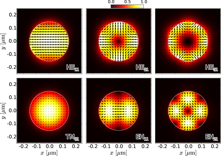
However, there is another important ingredient of the EOT that has not been considered much so far. When the size of the hole occupies large portion of the unit cell, the higher-order waveguide modes would play an important role. These higher-order waveguide modes as shown in Figure 1 have multipole nature that weakens the coupling with incident light that has a dipole nature and hence leads to having a minor contribution to the transmission spectra. Nonetheless, it is known that the combination of a bright dipole mode and a dark multipole mode yields to a sharp peak structure in the transmission spectra via Fano resonance that focuses much attention because of the expectation of potential applications such as the high-resolution bio-sensors Genet et al. (2003); luk’yanchuk et al. (2010). Therefore, it is expected that a variety of sharp resonance structures will appear in the transmission and reflection spectra due to the existence of higher-order waveguide modes Liu .
Moreover, it is expected that the multipole modes in the nanoholes are combined with each other by the SPPs on the film surfaces. In other words, the SPPs are combined by the multipole modes to produce novel type of hybridized bound modes which may be called as multipole surface plasmons (MSPs). The band structure of MSPs should have a distinct feature that is rarely seen in the lattice of dipoles such as the natural crystal of atoms with higher order of atomic orbitals that generates various structures of diverse physical properties.
In this paper, we investigate the contribution of multipolar waveguide modes of nanoholes to the creation of quasi-bound EM modes for the arrays of nanoholes perforated in thin gold film. In order to confirm the existence of MSPs, we have performed a thorough numerical simulation by using the rigorous coupled wave analysis (RCWA) method, which gives almost exact results of transmission, reflection and absorption spectra and also dispersion of quasi-bound modes. The contribution of the higher-order waveguide modes and their multipolar field distribution on the band structure of MSPs are further analyzed through the use of the coupled mode (CM) method.
II Method
We adopt two different theoretical approaches, namely, the RCWA method Li (1997); Weiss (2011) and the CM method García-Vidal et al. (2010); de León-Pérez et al. (2008). The accuracy of the results obtained from the use of our homemade numerical codes are checked through comparison with those obtained by the finite-difference time-domain (FDTD) method Taflove and Hagness (2005) with the help of a freely available software package Oskooi et al. (2010). In this section we present the basic ingredients of these two methods and explain their efficiency in obtaining the dispersion relations of the quasi-bound modes.
II.1 RCWA method
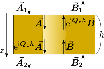
The RCWA method is applicable to systems that can be separated effectively into several planar layers. Each layer is invariant under translation in the thickness direction which is assumed to be in the -direction and is periodic in two other spatial directions (- and -directions). The fields in each layer are expanded in Fourier-Bloch modes that propagate or decay either forward or backward in the -direction. We can derive the solution of a stack of layers in a scattering matrix formalism. Scattering matrix provides a relation between the coefficient vectors and for the input modes and the coefficient vectors and for the output modes as shown below:
| (1) |
where the vectors () with being 1 or 2 contain a set of coefficients that define the amplitude and phase of the EM modes propagating in the () directions at the top () or bottom () interfaces (see Fig. 2). In this method, all the EM modes are expressed by the coefficient vectors with the same number of dimensions that are determined by the number of Fourier-Bloch modes used in the expansion. Likewise, the scattering matrix can be constructed iteratively for the stack of any number of layers considering the propagation in each layer and the boundary conditions at the interfaces Weiss (2011). Conversely, the truncation of Fourier series with a finite value of causes serious problem of poor convergence when there is any discontinuous jump in the permittivity distribution. Although the convergence can be improved using the so-called Fourier factorization rules Li (1997), the improvement is not enough in the case of metallo-dielectric structures since the difference between the permittivity of the metallic and the dielectric area is quite large. Therefore, we adopt the scheme of matched coordinates developed by Thomas Weiss Weiss (2011), in which the spatial resolution is increased adaptively close to the jump discontinuities with the application of the Fourier factorization rules by introducing a coordinate transformation technique developed at the beginning of transformation optics Pendry et al. (2006); Leonhardt and Philbin (2010). (Figure S1 in the Supplemental Material Sup shows the coordinate we used for the triangular lattice of nanoholes).
From the comparison with the results obtained by the FDTD method, we see that the RCWA method gives almost exact results for the transmission and reflection spectra (see Figure S4 in the Supplemental Material). Throughout our calculations, we used Fourier-Bloch modes. Figure S5 in the Supplemental Material shows that converging behavior is obtained around this number of Fourier-Bloch modes, and the expected error is small enough. The computational time required in the RCWA method is significantly shorter than that required to obtain quantitative results by the FDTD method.
II.2 CM method
In the CM method, the EM fields in the metallic nanohole array region are expressed only by the waveguide modes of the nanoholes. Imposing the continuity condition of EM fields at the openings of the holes and the surface impedance boundary conditions (SIBCs) Jackson (1999) at the surfaces of the metal film, we can derive a coupled system of equations for the coefficient vectors as follows:
| (2) | |||
where () is the coefficient vector for the waveguide modes propagating in the () direction at the top (bottom) interface. The matrix controls the EM coupling between waveguide modes at the interfaces, and denotes the diagonal matrix whose each diagonal element is the propagation constant associated with mode . The thickness of the metal film is denoted by while the vector takes into account the direct initial illumination over the waveguide modes. The mathematical expressions for the different magnitudes can be found in the Appendix.
At this point, we extend the original formulation García-Vidal et al. (2010) in two aspects in order to improve its quantitative aspect: (i) waveguide modes for a real metal with finite permittivity are used for the calculation of the overlaps of modal wavefunctions with plane waves, while PEC waveguide modes were approximately used in the original treatment and (ii) the admittance operator is introduced in order to express the orthogonality condition for the general hybrid modes having both TE and TM components.
Based from the results of the comparison made with the RCWA and FDTD methods, we have shown that our modifications have improved the CM method enough to give the quantitative prediction of the whole resonant structure in the transmission and reflection spectra with a computational time that is four orders of magnitude shorter than that required by the FDTD method (see Figure S2-S4 in the Supplemental Material Sup ). Throughout our calculations, we used 91 Fourier-Bloch modes whose wavenumbers are not exceeding 5 times the magnitude of the basic reciprocal lattice vector. Figure S6 in the Supplemental Material shows that converging behavior is obtained around this number of Fourier-Bloch modes, and the expected error is small enough to obtain quantitative results.
By the mean field approximation for the admittance operator, we can derive a similar expression as the original CM equations:
| (3) | |||
where (’) approximately represents the modal amplitude of the electric field at the top (bottom) interface. The mean field approximation deviates considerably from the exact calculation in the metal region near the hole edge as we can see from the in-plane magnetic field distributions shown in the Figure S7 of the Supplemental Material. However, the overlaps with plane waves are predominantly determined by the integral in the hole region, the influence on the spectra is not significant as we can see in the Figure S3 of the Supplemental Material.
II.3 Quasi-bound mode
The occurrence of resonant transmission implies the existence of a quasi-bound mode in the scattering object. Quasi-bound modes are solutions of Maxwell’s equation that can oscillate in time and hold EM energy within the object for a considerable period of time in the absence of incident light. Formally, we would have to derive a non-vanishing output for zero input.
In the RCWA method, this means that the quasi-bound modes would correspond to the output vectors and of Eq. (1) for zero input vectors and . In other words, the vectors and must be enlarged infinitely by the scattering matrix . Numerically, the search for quasi-bound modes can be fulfilled by seeking the infinite singular values of using the routine of singular value decomposition.
While in the CM method, the quasi-bound modes would agree to the non-trivial solutions of Eq. (2) for zero input vector , and thus we seek the eigenvectors of zero eigenvalue (i.e. null space) of the matrix .
In searching for the quasi-bound modes, we must take special care of the boundary condition at infinity. Quasi-bound modes are not true bound modes since they have finite lifetime as they eventually lose energy due to the weak emission in the absence of incident light. Therefore, we must seek the EM eigenmodes in the lower half of the complex plane of angular frequency , adopting the out-going-wave boundary condition. This means that one of the branches of the multi-valued function must be chosen obeying the condition that for or for . Certainly, this condition becomes nonphysical such that (i) mode fields explode at infinity (i.e. ) for the modes predominantly propagating to infinity and (ii) energy flows come from infinity (i.e. ) for the predominantly evanescent modes Taylor (1972).
III Results
III.1 Transmission, Reflection and Absorption Spectra
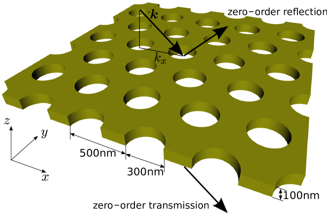
The system that we are concerned in this paper is a triangular lattice of nanoholes perforated in a thin gold film with a thickness of nm as shown in Figure 3. The film is surrounded with water. The diameter of the hole is assumed to be 300nm and the period of array, , is 500nm. The incident light is assumed to be a p-wave, and the component of the wave vector parallel with the film surface is in the direction, which is parallel to one of the lattice vectors.
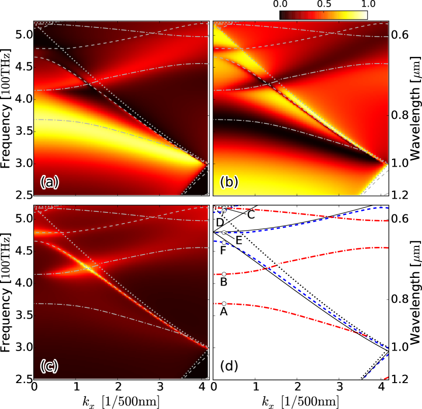
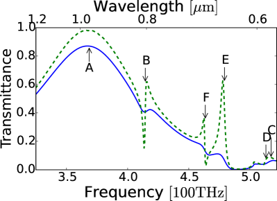
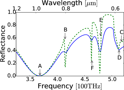
Figure 4 shows the spectra of (a) zero-order transmission, (b) zero-order reflection and (c) total absorption. These results were obtained by numerical simulation based on the RCWA method. The panel (d) shows the dispersion relation of the quasi-bound modes (red dash-dotted and blue dashed lines) together with the Rayleigh anomaly (dotted lines) and the dispersions of SPPs estimated using empty-lattice approximation (black solid lines). The dispersion of the quasi-bound modes and the Rayleigh anomaly are also shown in the panels (a)-(c) by gray dashed (or dash-dotted) lines and gray dotted lines respectively. At this point, we can clearly see the coincidence between resonant peaks or dips in the spectrum and the dispersions of quasi-bound modes. Although there is an abrupt change on the line of the Rayleigh anomaly, the profile of this change is still quite different. Hence, we conclude that the resonant structure of spectra is produced by quasi-bound modes.
Furthermore, we can also see that there are crossing points between red and blue lines. This means that there are two kinds of modes which cannot couple with each other due to the difference in symmetry. Since these two modes contribute independently to the absorption, it is expected that the total absorption would become high at the crossing points. Indeed, at the crossing point between the blue line passing through the point F and the red line passing though the point B, the total absorption rate becomes quite high, to about more than 90% as shown in the panel (c).
III.2 Bonding and Anti-bonding Bound Modes
As we pointed out in the last subsection, there are two types of branches as represented by the red dash-dotted lines passing through points A, B and C and blue dashed lines passing through points D, E and F in the panel (d) of Figure 4. The blue dashed lines are almost in accordance with the black solid lines, which indicate the empty-lattice bands of SPPs, while the slope of the red dash-dotted lines are rather shallow.
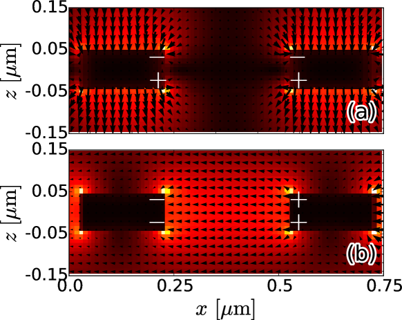
Figure 5 presents the electric field distributions in the plane (a) at point F and (b) at point A as shown in the panel (d) of Figure 4. From the panel (a), we see that the charge distribution is anti-symmetric about the plane, and the intensity of the electric field strengthens mainly outside of the metal surfaces between the holes. On the other hand, from the panel (b), we see that the charge distribution is symmetric about the plane and the intensity of the electric field concentrates around the holes, specifically inside of the metal film region. These features indicate that the modes on the blue lines are anti-bonding (AB) modes in which the SPPs of both sides of the gold film are combined anti-symmetrically like a long-range SPP of a thin metal film Sarid (1981). On the other hand, the modes on the red lines are bonding (B) modes like a short-range SPP of a thin metal film. The symmetry of each bound mode can be checked clearly using the CM method. The dispersion relations of B-SPP and AB-SPP calculated using the CM method (Eq. (2)) under the symmetric ( and anti-symmetric () conditions are shown in Figures 7 and 8, respectively.
In the AB-SP where the electric field is expelled from the hole area, each SPP propagates on each surface without feeling much of the holes. This in turn makes the dispersions sit near the empty-lattice bands. We can also see that the resonant structure of the spectra created by AB-SPP is narrow due to the darkness of the mode. On the other hand, the B-SPP has large contribution from the waveguide modes in the holes and the dispersions are shifted largely from the empty-lattice bands. The shallowness of the band indicates that the B-SPP is much like a cavity mode whose electric field is confined in the nanoholes.
The lowest energy B-SPP mode can also be considered as a coupled spoof surface plasmon, since the dispersion saturates around the cutoff frequency of the HE11 mode, 355 THz. But then what are higher energy B-SPP modes? These modes may be considered as coupled multipole spoof surface plasmons which are geometrically induced coupled surface modes created by the coupling between the SPP on the metal surface and the higher order waveguide modes of the nanoholes as discussed in the next subsection.
III.3 Multipole Nature of Bound Modes
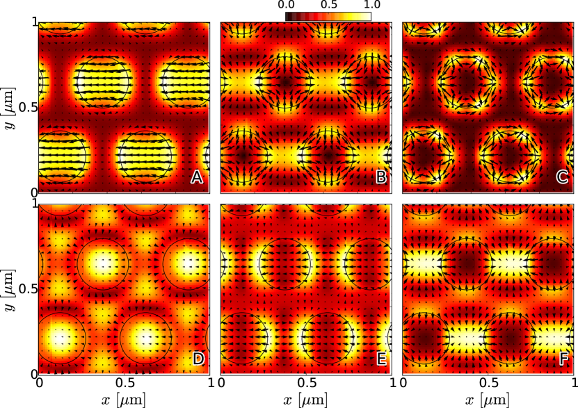
Figure 6 shows the electric field distributions at 20nm above the surface of the gold film for the quasi-bound modes at the points shown in Figure 4(d). We can see monopole (D), dipole (A, E), quadrupole (B, F) or hexapole (C) texture for each branch of the quasi-bound modes. The most striking feature is that a strong coupling between adjacent holes seems to exist in the quadrupole texture (B, F) as well as positive charges are aligned in the -direction to form a stripe texture.
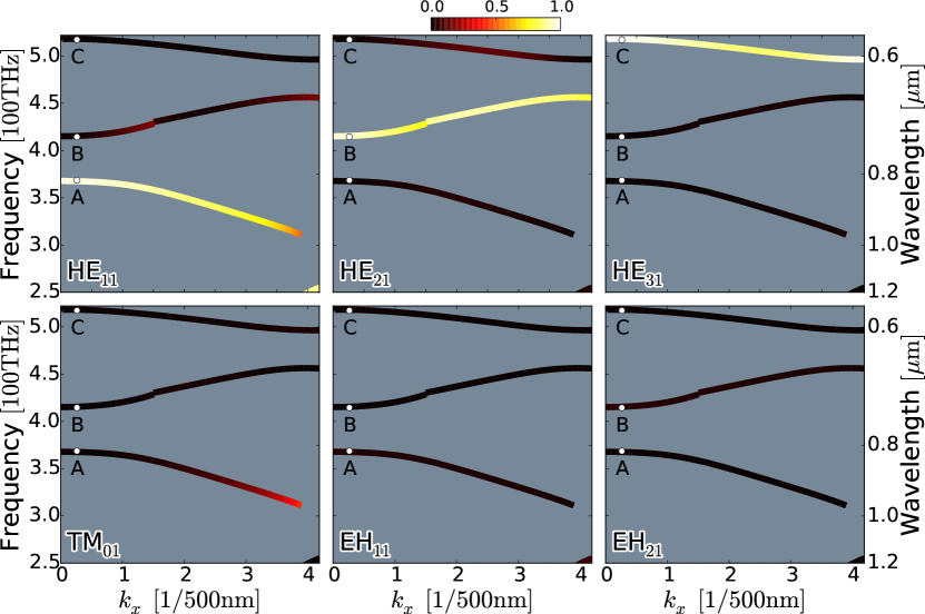
In order to see the role played by the waveguide modes to create these multipole textures, we have analyzed the contribution of waveguide modes for each branch using the CM method. Figure 7 shows the rate of contribution of the waveguide mode whose name is written at the bottom left corner of each panel. The bright color means that the rate of contribution of the mode is high. It is clearly seen that each branch of the B-SPPs namely, A, B and C is mainly created by a single waveguide mode, HE11, HE21 or HE31 respectively. This means that the coupled spoof surface plasmon yields higher energy branches with multipole textures according to the higher order waveguide modes.
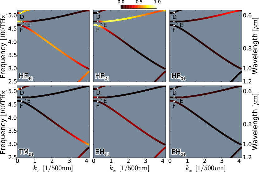
The contribution of the waveguide modes to the AB-SPPs is more complicated. There is non-negligible contribution from the TM-like modes, i.e. TM01 and EH11. Furthermore, a kind of band inversion seems to occur between two bands produced by HE11 and HE21 modes. The contribution rates of HE11 and HE21 modes are reversed around the points E and F. This could be explained as a result of band anti-crossing arising from the band inversion between HE11 and HE21 bands near the point.
In order to reveal the origin of these band structures, we approximately analyze the dispersion relation of the quasi-bound mode produced by a single waveguide mode either from HE11 or HE21. This is done using a metamaterial treatment as in García-Vidal et al. (2010), where only a single mode inside the hole is taken into account and only the p-polarized zero-order diffraction mode is considered in the quantity governing the coupling between holes. Starting with the mean-field approximated CM equations (3), we obtain the condition for the existence of B-SPP mode as where , , and . The definitions of the symbols can be found in the Appendix. Neglecting the imaginary part of the permittivity of gold , the dispersion relation of the bonding quasi-bound mode is given by
| (4) |
From Eq. (4), we can see that the dispersion relation is reduced to that of the SPP on the flat gold surface within the SIBC approach, , if the coupling between the waveguide mode and the diffraction mode is negligibly small . On the other hand, as the frequency approaches the cutoff frequency from below, diverges for HE modes since HE modes approach TE modes and the effective admittance goes to zero as goes to zero. Correspondingly, goes to in this limit. Although the absorption of gold prevents from diverging, this divergence property remains and the dispersion relation flattens around the cutoff frequency as long as the film remains thin.
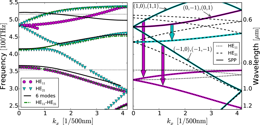
The right panel of Figure 9 shows the dispersion relation of Eq. (4) considering the diffraction effects in the empty-lattice limit. We can see that the dispersion curves, dotted lines and dashed lines, converge to the cutoff frequencies of HE11 mode (355THz) and HE21 mode (516THz), respectively. In this panel, the empty-lattice bands of the SPPs on a flat gold surface are also shown by black solid lines. The set of numbers indicates the diffraction order which mainly contributes to the branch pointed by the arrow. The parallel momentum for the diffraction order is described by the expression where and are the reciprocal lattice vectors for the triangular lattice of the period given by . Therefore, the branches for the diffraction orders , , and are composed of the EM wave with a period equal to , such that
Also, the branch for the diffraction orders and is composed of the EM wave with a period equivalent to /2, where
These periodicities in the -direction are considered to play a major role to produce the bands of B-SPPs. The left panel of Figure 9 shows the dispersion relations calculated by the mean-field approximated CM equations (3) including only a single waveguide mode either HE11 (magenta circles) or HE21 (cyan triangles) but with the presence of as many diffraction modes as needed to achieve convergence. Taking into account the fact that the dispersion relation moves closer to the light line if higher-order diffraction modes are included García de Abajo and Sáenz (2005); Hendry et al. (2008), it is reasonable to think that the branches of B-SPP bands created by HE11 mode are composed of two types of branches: (i) the periodic branches from the flat-surface SPP bands that correspond to the black solid lines in the right panel and (ii) the /2 periodic branches from the bands of coupled spoof surface plasmons that represent the dotted lines in the right panel. The diffracted waves with periodicity may couple strongly with the dipole lattices created by HE11 mode. In effect, coupled spoof surface plasmons are formed and dispersion relation are put downward since positive and negative charges align alternately in the -direction to form periodic texture as you can see in Figure 6 A. Besides, the diffracted waves with /2 periodicity may couple strongly with the quadrupole lattices created by HE21 mode since positive or negative charges produce bond between adjacent holes to form stripe texture with /2 periodicity as you can see in Figure 6 B. Considering the couplings between HE11 and HE21 or with higher order waveguide modes, the texture seems to be optimized and yield simpler band structure (see green dash-dotted lines and black solid lines in the left panel).
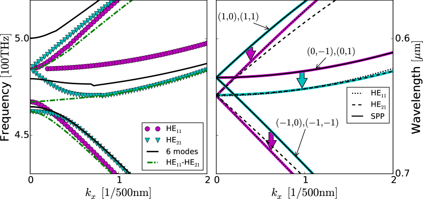
The dispersion relation of the AB-SPP mode is obtained by replacing with in Eq. (4) as shown in the right panel of Figure 10. In this case, the influence of the coupling between waveguide mode and diffraction modes become weak as becomes small. The results for the film with nm are shown in figure for clarity. The left panel shows the dispersion relations of AB-SPP obtained with the same procedure as used in the left panel of Figure 9. These results are seemingly produced by the same mechanism as those of B-SPP: only the (/2) periodic branches are put downward due to the periodicity of the dipole (quadrupole) texture for the HE11 (HE21) mode. Therefore, the multipole textures are the origin of the band inversion and anti-crossing between HE11 and HE21 bands.
III.4 Fano Resonance
As mentioned above, the AB-SPPs and the higher energy B-SPPs have multipole nature, which can be considered as dark modes. The peak and dip structures in the spectra would be attributed to the Fano resonances between the brighter modes and the darker modes. Indeed, if the loss of gold is low to about 10% of the normal loss, then we can clearly see a typical asymmetric Fano structures that consist of pairs of peak and dip at nearby frequencies Genet et al. (2003); luk’yanchuk et al. (2010) as shown in Figure 11.
Thus, the complicated and distinct structure in the transmission and reflection spectra of this system can be attributed to the Fano resonances between various orders of multipole surface plasmons.
IV Conclusion
By thorough numerical simulations using RCWA and CM methods, we have found that the higher order waveguide modes of nanoholes combine the two SPPs at both sides of metal film to create two types of quasi-bound EM modes. These are the (i) AB-SPP with anti-symmetric charge distribution and (ii) B-SPP with symmetric charge distribution about the center plane of the film. Due to the multipole nature of the waveguide modes, the electric field distribution near the film surface forms a multipole texture. The Fano resonances between various orders of these multipole surface plasmons produce sharp peak-dip structure in the transmission and reflection spectra.
The B-SPP modes can be considered as coupled multipole spoof surface plasmons whose electric fields are mainly confined in the nanohole region and the waveguide modes play a major role in determining their dispersions. In other words, the nanoholes act like artificial atoms and the multipolar EM wave in a hole hops to other hole via SPPs just like the electron in a lattice of real atoms that have higher atomic orbitals. More so, the dispersion of the AB-SPP mode is determined by the combination of multiple waveguide modes which yields a fine band structure due to the band inversion and anti-crossing induced by the multipole textures.
Further study of these two types of multipole surface plasmons will open the possibility to create various artificial materials with high functionality utilizing their high degrees of freedom, e.g. a perfect absorber using multiple crossing points of the band structure or a high-resolution bio-sensor using multiple resonant transmissions.
Appendix A Coupled-Mode Method for Real Metal
In general, the mode fields of a waveguide that is composed of a piecewise homogeneous media can be expressed as a linear combination of TE and TM components, such that
| (5) | ||||
| (6) |
where and are the electric and magnetic field vectors that are respectively projected onto the -plane. Also, is a unit vector along the -axis and y) is the position vector in the -plane. Here, the mode index represents the full information of the waveguide mode of a nanohole in the metal film region, such as the “HE11 horizontal mode” Roberts (1987). It may also represent the parallel momentum and the polarization for plane-wave modes in the homogeneous dielectric layers where 0) or . The position-dependent admittances for the TE and TM modes are piecewise constants whose values in the th homogeneous medium are given by
| (7) | ||||
| (8) |
where and are the impedance and the wavenumber in the vacuum, and are the relative permittivity and relative permeability in the th homogeneous medium, and is the propagation constant of the mode . This representation indicates that the magnetic field of a mode is constructed by a position-dependent admittance from the corresponding electric field. If we use Dirac’s notation to describe the electric field, such that
| (9) |
the effect of the position-dependent admittance is expressed by the admittance operator which maps the electric field to the corresponding magnetic field, such that
| (10) |
The orthogonality condition for the modes can be expressed by the admittance operator as
| (11) | ||||
| (12) |
where is the Kronecker delta and denotes the complex conjugate.
Using this definition of the admittance operator, the CM equation (2) can be derived in a similar manner as the original derivation de León-Pérez et al. (2008). The component of the coefficient vector and the component of the matrix that appeared in Eq. 2 are expressed as
| (13) | ||||
| (14) |
Here, we introduced an operator which has an expectation value for plane waves using the surface impedance
| (15) |
with and being the relative permittivity and the relative permeability of the metal. Additionally, the transmission and reflection coefficients are expressed as
| (16) | ||||
| (17) |
where () is the coefficient for the mode propagating in the () direction at the top (bottom) interface, and denotes the film thickness.
If we adopt a kind of mean-field approximation for the admittance operator, such that
| (18) | ||||
| (19) |
and introduce the modal amplitudes of the electric field at the top and bottom interfaces as
| (20) | ||||
| (21) |
then the CM equations can be expressed as Eq. (3). The component of the matrices , and are given as
| (22) | ||||
| (23) | ||||
| (24) |
The details of the derivation will be published in another avenue.
Acknowledgements.
This work was supported in part by KAKENHI No. 23651149 from MEXT of Japan.References
- Ebbesen et al. (1998) T. W. Ebbesen, H. J. Lezec, H. F. Ghaemi, T. Thio, and P. A. Wolff, Nature 391, 667 (1998).
- García-Vidal et al. (2010) F. J. García-Vidal, L. Martín-Moreno, T. W. Ebbesen, and L. Kuipers, Rev. Mod. Phys. 82, 729 (2010).
- Lalanne et al. (2005) P. Lalanne, J. C. Rodier, and J. P. Hugonin, Journal of Optics A: Pure and Applied Optics 7, 422 (2005).
- Bethe (1944) H. A. Bethe, Phys. Rev. 66, 163 (1944).
- Roberts (1987) A. Roberts, J. Opt. Soc. Am. A 4, 1970 (1987).
- Pendry et al. (2004) J. B. Pendry, L. Martín-Moreno, and F. J. Garcia-Vidal, Science 305, 847 (2004).
- Martín-Moreno et al. (2001) L. Martín-Moreno, F. J. Garcia-Vidal, H. J. Lezec, K. M. Pellerin, T. Thio, J. B. Pendry, and T. W. Ebbesen, Phys. Rev. Lett. 86, 1114 (2001).
- Ruan and Qiu (2006) Z. Ruan and M. Qiu, Phys. Rev. Lett. 96, 233901 (2006).
- García-Vidal et al. (2005) F. J. García-Vidal, E. Moreno, J. A. Porto, and L. Martín-Moreno, Phys. Rev. Lett. 95, 103901 (2005).
- Wood (1902) R. Wood, Phil. Mag. 4, 396 (1902).
- Sarrazin et al. (2003) M. Sarrazin, J.-P. Vigneron, and J.-M. Vigoureux, Phys. Rev. B 67, 085415 (2003).
- Rayleigh (1907) O. M. L. Rayleigh, Proc. R. Soc. Lond. A. 79, 399 (1907).
- Hessel and Oliner (1965) A. Hessel and A. A. Oliner, Appl. Opt. 4, 1275 (1965).
- Genet et al. (2003) C. Genet, M. van Exter, and J. Woerdman, Optics Communications 225, 331 (2003).
- luk’yanchuk et al. (2010) B. luk’yanchuk, N. I. Zheludev, S. A. Maier, N. J. Halas, P. Nordlander, H. Giessen, and C. T. Chong, Nature Mater. 9, 707 (2010).
- (16) The contributions of multipolar resonances to the transmission suppression effect in a perforated ultrathin metallic film have been investigated in M. Liu, Y. Song, Y. Zhang, X. Wang, and C. Jin, Plasmonics 7, 397 (2012).
- Li (1997) L. Li, J. Opt. Soc. Am. A 14, 2758 (1997).
- Weiss (2011) T. Weiss, Advanced numerical and semi-analytical scattering matrix calculations for modern nano-optics, Ph.D. thesis, University of Stuttgart (2011).
- de León-Pérez et al. (2008) F. de León-Pérez, G. Brucoli, F. J. García-Vidal, and L. Martín-Moreno, New J. Phys. 10, 105017 (2008).
- Taflove and Hagness (2005) A. Taflove and S. C. Hagness, Computational Electrodynamics: The Finite-Difference Time-Domain Method, 3rd ed. (Norwood, MA: Artech, 2005).
- Oskooi et al. (2010) A. F. Oskooi, D. Roundy, M. Ibanescu, P. Bermel, J. D. Joannopoulos, and S. G. Johnson, Computer Physics Communications 181, 687 (2010).
- Pendry et al. (2006) J. B. Pendry, D. Schurig, and D. R. Smith, Science 312, 1780 (2006).
- Leonhardt and Philbin (2010) U. Leonhardt and T. Philbin, Geometry and Light: The Science of Invisibility (Dover Publications, 2010).
- (24) See Supplemental Material for additional figures.
- Jackson (1999) J. D. Jackson, Classical Electrodynamics 3rd ed. (Wiley, New York, 1999).
- Taylor (1972) J. R. Taylor, Scattering Theory (John Wiley & Sons, New York, 1972).
- Sarid (1981) D. Sarid, Phys. Rev. Lett. 47, 1927 (1981).
- García de Abajo and Sáenz (2005) F. J. García de Abajo and J. J. Sáenz, Phys. Rev. Lett. 95, 233901 (2005).
- Hendry et al. (2008) E. Hendry, A. P. Hibbins, and J. R. Sambles, Phys. Rev. B 78, 235426 (2008).