Towards improved exact exchange functionals relying on GW quasiparticle methods for parametrization
Abstract
We use fully self-consistent GW calculations on diamond and silicon carbide to reparametrize the Heyd-Scuseria-Ernzerhof exact exchange density functional for use in band structure calculations of semiconductors and insulators. We show that the thus modified functional is able to calculate the band structure of bulk Si, Ge, GaAs, and CdTe with good quantitative accuracy at a significantly reduced computational cost as compared to GW methods. We discuss the limitations of this functional in low-dimensions by calculating the band structures of single-layer hexagonal BN and MoS2, and by demonstrating that the diameter scaling of curvature induced band gaps in single-walled carbon nanotubes is still physically incorrect using our functional; we consider possible remedies to this problem.
I Introduction
Applied materials science relies heavily on the ability of theoreticians to accurately predict the physical properties of novel materials. Calculations are widely used as guidance in the design of new materials, without which experiments can rapidly turn into a cumbersome and expensive trial-and-error process. Unfortunately, the ability of theoreticians to provide guidance to experimentalists is in practice severely limited by the accuracy of the methods available. One particular example for this issue is the problem of predicting the band gap of semiconductors.
A widely used and very accurate method in the study of semiconducting materials is density functional theory (DFT). Useful as it is, a well known problem exists with DFT in that it severely underestimates the band gap. This is especially true in low-dimensional materials such as boron nitride Topsakal et al. (2009), polyyne Rusznyák et al. (2005); Al-Backri et al. (2014), or even carbon nanotubes where even the diameter scaling of the curvature induced band gap is wrong, let alone its magnitude Zólyomi and Kürti (2004). This problem can be circumvented by going beyond the DFT level and using for example the Quantum Monte Carlo (QMC) method to calculate the band gap Needs et al. (2010). QMC is however extremely expensive to apply to semiconductors or insulators unless the location of the band gap in the reciprocal space is exactly known.
Another approach for improving the band gap is the use of many-body theory, and more specifically, the GW approximation Hedin (1999). This allows one to calculate the quasiparticle band structure by starting from the DFT wave functions and solving the Dyson equation. The resulting band gaps are typically in very good agreement with experiments and are a signifcant improvement over DFT results (see Figure 1). The disadvantage of the GW approximation is that it is computationally very expensive. While today it is possible to use the method on systems composed of as much as a hundred atoms on massively parallel machines Deslippe et al. (2012), there are plenty of calculations that are simply not feasible with GW to this day. Examples include large supercell calculations such as surface intercalation, or the study of composite materials and heterostructures, which are of particular interest to the scientific community Britnell et al. (2012, 2013); Fiori et al. (2013). Furthermore, in low-dimensional materials the GW approach converges extremely slowly as pointed out in a recent publication Qiu et al. (2013), making it all but infeasible for the study of nanoscale materials at this time.
Due to the computational expense of both QMC and GW calculations, it would be advantageous to develop a computational method that is able to approach the accuracy of QMC or the GW approximation without the accompanying computational expenses. The trivial choice would be the use of exact exchange density functionals, also known as hybrid density functionals. These are known to predict a much more accurate band gap than traditional density functionals such as the local density approximation (LDA) or the semilocal Perdew-Burke-Ernzerhof (PBE) generalized gradient approximation (GGA) as well as other GGA functionals. While exact exchange functionals still underestimate the band gap, and they in general suffer from serious problems in terms of predictive power as pointed out recently Jain et al. (2011), in principle it is possible to modify the parameters of these functionals in order to deliver a better accuracy when calculating the band structure.
Screened exact exchange functionals such as the Heyd-Scuseria-Ernzerhof (HSE) functional include dielectric screening Heyd et al. (2006) which makes them ideal for use in periodic structures including three dimensional solids and low-dimensional materials like carbon nanotubes. These functionals offer two easily accessible parameters that can be adjusted without tampering with the core of the functional: these are the amount of exact exchange, and the screening parameter. Adjusting these parameters is possible using a variety of criteria, including what has been dubbed the HSE12 functional Moussa et al. (2012). For the purposes of accurate band structure calculations it is sensible to set the criteria to achieve the best possible match between the band structures predicted by the modified HSE functional and GW many-body theory.
In this work we present a modification to the HSE functional with the help of fully self-consistent GW many-body calculations. As we show below, it is possible to adjust the two parameters in the HSE functional such that the band structures calculated with the modified functional are in very close agreement with GW calculations. We compare our modified HSE functional to the HSE12 functional. We argue that our method makes quantitatively accurate first-principles band structure calculations on large systems feasible. The method is of course not without its own limitations, which we discuss at the end of the paper.
II The modified HSE functional
In our calculations we rely on the VASP code Kresse and Furthmüller (1996), using a plane-wave basis set. Our goal is to develop an exact exchange functional that reproduces the GW quasiparticle band gaps in semiconductors. We use the Heyd-Scuseria-Ernzerhof 2006 (HSE06) functional as the basis for this approach, which describes the exchange part of the density functional as 25% exact exchange and 75% PBE exchange. The modified functional differs from the original HSE06 in two parameters only, the amount of exact exchange and the screening parameter. The new parameters are obtained by performing a least squares fit between the band structures obtained with our functional and GW band structures, then changing the parameters until the root mean square (RMS) is found to be minimal.
The fitting procedure is performed using the highest valence and lowest conduction bands in the entire Brillouin zone on a finite, -point grid. At each -point the squared energy difference is taken between the GW and the modified HSE valence band, then summed up over the entire grid. The process is repeated for the conduction band and added to the sum obtained from the valence band. The thus obtained RMS value gauges the quality of the match between the modified HSE functional and the GW calculation. The smaller the RMS the better the parameters of the modified HSE functional.
The GW calculations are performed in the fully self-consistent approach where both the Green’s function and the dielectric screening are iteratively updated until self-consistency is reached (a maximum of four iterations were required). This allows for the best available accuracy within GW many-body theory. Considering the difficulty of converging such calculations in low-dimensional materials Qiu et al. (2013) we restrict ourselves to three-dimensional crystals. In particular we look at diamond and silicon carbide (3C-SiC) crystals. The geometries are optimized using the HSE06 functional. The GW calculations are then performed in fixed geometries. Both the structural relaxations and the GW calculations are carefully tested for convergence with respect to a variety of parameters. The convergence criteria used here are an uncertainty of Å in the lattice constant during the HSE06 optimizations and an uncertainty of eV in the energy gap during the GW calculations. The HSE06 optimizations are found to reach convergence at an Monkhorst-pack grid in -space and 800 eV plane-wave cutoff energy, while the GW calculations at a -point grid, 400 eV plane-wave cutoff, 16 electronic bands, and where is the number of frequency points used in the contour integrations in the complex plane.
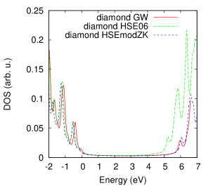
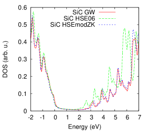
With the fully converged GW band structures available we can make an easy comparison between many-body theory and existing hybrid density functionals. Figure 1 shows the electronic density of states for diamond and silicon carbide according to the GW approximation and the HSE06 functional. As expected the HSE06 band gap is much smaller. If, however, we modify the exact exchange ratio and screening parameters in the HSE06 functional, it is possible to rectify this problem.
We shall denote the two parameters as follows. Parameter is the amount of exact exchange in the density functional, i.e. the total exchange in the functional is where and are the exact and PBE exchange terms, respectively. Parameter controls the amount of screening in the functional; the dimension of is inverse length and it determines the separation of long– and short–range terms in the exchange within HSE-type functionals, which is equivalent to applying a semiempirical screening to long–range interactions. In our starting point, the HSE06 functional, and Å-1. In order to modify the HSE functional to fit the band gap to that found in GW many-body theory, we explore this two-dimensional parameter space within the range of and Å-1. The previously discussed RMS will be a function of these two parameters, and in order to find the ideal settings for and this function must be minimized.
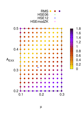
Figure 2 shows the RMS of the least square fit between the GW band structures and the modified HSE functional as a function of and , averaged for diamond and silicon carbide, the two benchmark materials considered. The entirety of the topmost valence band and the bottommost conduction band is taken into account spanning the entire Brillouin zone in a grid. The best fit is achieved at and Å-1. The figure highlights the settings of the original HSE06 functional, the HSE12 parametrization, and our modified HSE functional. As it can be seen, the fit substantially improves between our modification and either HSE06 or HSE12.
Now if we return to Figure 1 we can see that the density of states obtained using our modified HSE functional with and Å-1 agrees extremely well with the GW calculations for both diamond and silicon carbide.
III Application of the modified HSE functional
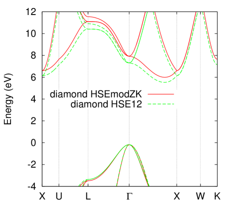
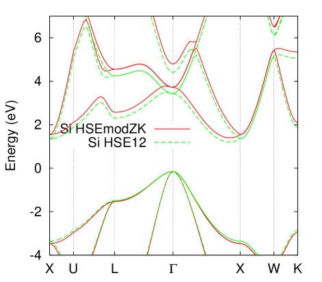
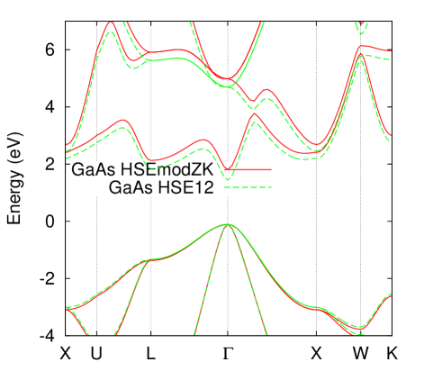
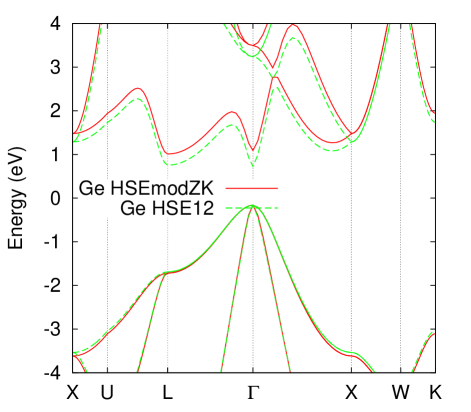
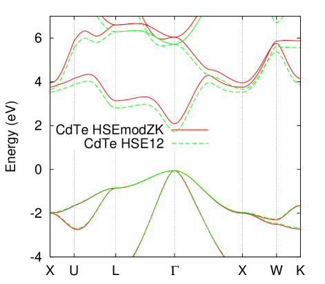
Now we turn our attention to the use of the modified HSE functional. First we look at its performance on three-dimensional semiconductors, bulk silicon (Si), germanium (Ge), gallium arsenide (GaAs), and cadmium telluride (CdTe). Figure 3 shows the band structures of these four materials using our modified HSE functional, along with those of diamond and silicon carbide. Table 1 compares their band gaps with our GW calculations. The overall agreement is quite good, with the average absolute deviation between the band gaps in the modified HSE functional and our GW results being a modest 0.14 eV. This is a significant improvement on the average performance of the HSE12 functional which yields an average absolute deviation of 0.28 eV. We must note however that in some individual cases HSE12 performs better, such as bulk silicon.
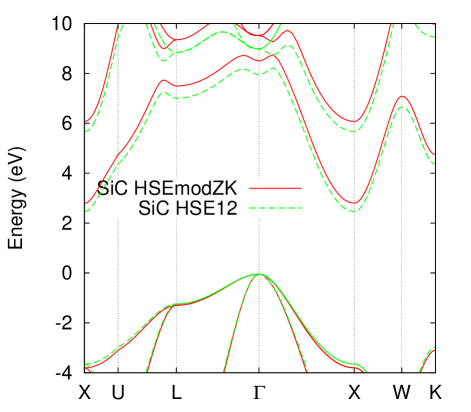
| C | 6.16 | 6.05 | 5.69 |
| Si | 1.55 | 1.33 | 1.35 |
| Ge | 1.17 | 1.07 | 0.89 |
| SiC | 2.84 | 2.70 | 2.50 |
| GaAs | 1.92 | 2.12 | 1.54 |
| CdTe | 2.14 | 2.08 | 1.76 |
We must note here that we use geometries obtained using the HSE06 functional for all our calculations. We do this because we cannot expect the modified functional to correctly predict the total energy or the Hellmann-Feynman forces. Density functionals are typically optimized to possess accurate predictive power for a broad range of physical properties, whereas our modified HSE functional is made specifically for the purposes of calculating accurate band structures in a fixed geometry. This does not necessarily mean that the HSE06 geometries will be good enough, as for example the diamond lattice constant is notably underestimated; this is discussed below.
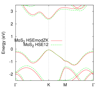
Now we turn to lower dimensional materials, starting with two-dimensional nanosheets. In particular we consider single layer molybdenum disulphide (MoS2) and hexagonal boron nitride (h-BN). Their band structures are shown in Figure 4, their band gaps are compared to previous GW literature in Table 2.
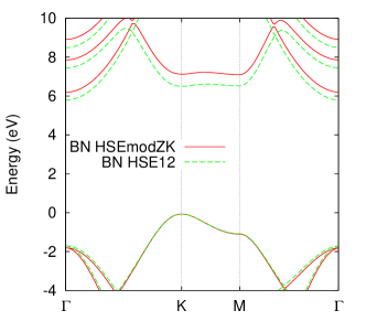
| BN | 6.26 | 7.0 Drummond et al. | 5.86 |
| MoS2 | 2.49 | 2.84 Qiu et al. (2013) | 2.42 |
Our band gap for MoS2 is 2.49 eV which compares reasonably to literature estimates of 2.50 eV and 2.66 eV quasiparticle gaps Shi et al. (2013) obtained using the single shot G0W0 and the partially self-consistent GW0 method, respectively, but is notably below the fully self-consistent GW band gap of 2.84 eV Qiu et al. (2013) (albeit the experimental lower bound for the quasiparticle band gap is 2.5 eV Klots et al. (2014)). The band gap of h-BN is found to be 6.26 eV here, which falls between recent predictions for the band gap Drummond et al. in HSE06 (5.65 eV) and single-shot G0W0 calculations (7.0 eV). While our functional significantly improves the band gap for both MoS2 and h-BN, it still underestimates the GW results. This suggests that care must be taken when applying our functional for the study of two-dimensional materials.
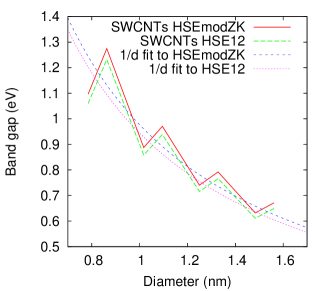
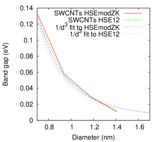
Finally we consider a more difficult problem, that of the curvature induced band gaps in carbon nanotubes. In single-walled carbon nanotubes (SWCNTs) the simple zone-folding picture predicts that whenever the difference between the chiral indices is a multiple of 3, the nanotube is metallic. In reality, the finite curvature of the SWCNT surface induces a band gap in all cases except for armchair SWCNTs. This means that zigzag nanotubes exhibit a small, curvature induced band gap when . This has been known for many years, and it has been measured in STM Ouyang et al. (2001) which has shown that the curvature induced band gap approximately scales as where is the diameter of the SWCNT. Indeed, being a curvature induced effect, this gap must scale with an even power of . DFT calculations however are unable to correctly reproduce this behavior. The LDA in fact predicts a scaling Zólyomi and Kürti (2004), which is a clear indication of the failure of semilocal density functional theory to accurately describe electronic excitations. Hence we use our modified HSE functional to recalculate the band structure of zigzag nanotubes in an effort to rectify this failing of semilocal DFT functionals.
Figure 5 shows the band gap of zigzag nanotubes from to , with the curvature induced gaps plotted separately in the lower panel, using both our modified HSE functional and the HSE12 functional. As it can be seen the diameter scaling of the curvature induced band gap still follows the scaling found in LDA calculations. This illustrates that the modified HSE functional is unfortunately not entirely suited for one-dimensional materials, and neither is HSE12. On the other hand, both functionals correctly capture the physics in the primary gaps of semiconducting zigzag nanotubes, as both the scaling of the gap and the trigonal warping related buckling effect are correctly described. The band gaps are larger in our modified HSE functional, as expected.
IV Discussion
We have demonstrated above that empirically fitting the parameters of HSE-type exact exchange functionals to GW calculations is a feasible and sound approach to improve the performance of such functionals in band structure calculations. We have in particular demonstrated that by changing the parameters of the HSE06 functional it is possible to calculate band structures that agree with GW calculations for the valence and conduction band with an average RMS error of 0.1 eV, which is very impressive for a density functional.
The importance of this finding cannot be stressed enough. A very simple modification enables one to use an HSE-type density functional to closely approach the accuracy of GW. Since HSE-type calculations are not only significantly cheaper than GW but are also much easier to converge, the modified HSE functional can be used to give accurate theoretical predictions for the band structure of the kind of complex materials where GW is simply not feasible. Therefore, a correctly parametrized modification of the HSE functional is invaluable for condensed matter research, and we have demonstrated here that such a parametrization is possible to find.
However, it is important to be aware of two shortcomings of this study. First of all, the band gaps obtained in our GW calculations are consistently higher than expected; this is especially notable in the case of diamond where our GW band gap is 6.05 eV while experimentally it is 5.47 eV. Previous G0W0 calculations performed on the experimental geometry yielded a much better match with a band gap of 5.68 eV Surh et al. (1992). Similarly, our GW band gaps for Si, Ge, and GaAs are notably larger than previous GW calculations Tiago et al. (2004). Considering that we rely on fully self-consistent GW rather G0W0 or GW0, this is a surprising result. One must bear in mind, however, that electron-phonon coupling introduces a notable band gap renormalization in diamond lattices. In particular, in diamond itself the gap is reduced by 0.4 eV Surh et al. (1992); Monserrat and Needs (2014); Monserrat et al. (2014), which accounts for most of our overestimation and leaves only an error of 0.18 eV unexplained.
This remaining difference may be due to a number of reasons. One may be the use of HSE06 geometries instead of experimental lattice constants. The lattice constant of diamond is slightly underestimated at a value of 3.54 Å in our calculations as opposed to the experimental value of 3.57 Å. However, the calculated lattice constant of silicon is 5.44 Å which matches the experimental 5.43 Å rather well, so the lattice constant may not be the biggest factor. Much more likely is that our calculations face convergence issues. This is a surprising finding since, as mentioned earlier in the paper, we have performed a full convergence test with respect to all relevant parameters in the calculation, and we have done so without separating them (that is, they were not treated independently). We have used direct energy gaps at high symmetry points in the Brillouin zone as the convergence criteria. Our finding was that these energies change less than eV when we try to exceed the converged parameter set.
One possibility is that the calculations have reached a local minimum in the parameter space of the GW parameters, and that we need to go much further for true convergence. In particular, it has been suggested that the number of empty bands should be on the order of a few hundred in diamond lattice materials such as silicon Tiago et al. (2004). On the other hand, the expectation is that the band gap will approach the converged value from below, while in our case the gap is overestimated. The reason for this discrepancy is currently unclear, although the next step is obviously to extend the convergence tests in the GW calculation to greater ranges in the parameter space. This, however, goes well beyond the scope of this work, since the calculations are significantly more expensive to perform if for example the number of bands taken into account is increased to a few hundred.
We emphasize that these potential convergence problems in our GW calculation do not impact the main message of our paper, namely that it is perfectly possible to fit an HSE-type exact exchange functional to GW calculations. The parameters of and Å-1 will no doubt need to be further adjusted before the modified HSE functional suggested here can be used for quantitative predictions of the band gap in semiconductors. In addition, in order to determine a final set of parameters to use in the modified HSE functional it would be advisable to perform the calculations over a large set of materials comprising lattices of different symmetries and atomic composition. The parameters in this paper should be used only as guidelines for future calculations.
There is a second issue with the modified HSE functional, that of its performance in low-dimensional materials. As our GW calculations seem to overestimate the gap in three-dimensional semiconductors, it is somewhat surprising to find that the modified HSE functional underestimates the band gap in the case of low-dimensional structures. The band gaps of MoS2 and monolayer boron nitride are both too small and the diameter scaling of curvature induced secondary gaps in SWCNTs is the same unphysical dependence as was found in LDA. One possible reason for this is that our functional is parametrized exclusively on three-dimensional crystals due to the difficulty in converging GW calculations in low dimensions. Strictly speaking the dielectric screening in a low-dimensional material is expected to be substantially different from that observed in three dimensions, hence in low-dimensional materials the screening parameter is expected to be different. As such, the finding that our modified HSE functional faces difficulties in low dimensions is not surprising.
The solution to the above problem is of course a reparametrization of the modified HSE functional for use in two– and one–dimensional materials. This requires a number of fully converged and fully self-consistent GW calculations to be performed on low-dimensional structures to act as benchmarks. These are very difficult to obtain as we have seen in the case of polyyne Al-Backri et al. (2014) and boron nitride Drummond et al. , and our current computational resources prohibit us from performing them. Nevertheless the relative success of our modified HSE functional in three dimensions indicates that this reparametrization is the next logical step towards improved exact exchange density functionals for use in electronic band structure calculations.
Finally we must note that, considering recently reported performance issues in exact exchange functionals Jain et al. (2011), it is quite possible that such density functionals cannot accurately predict the curvature induced gaps of SWCNTs at all. The qualitative agreement between the HSE12 functional and our modified HSE functional in the case of the curvature induced gaps of SWCNTs further suggests that this may be the case. In order to convincingly answer this question it would be necessary to not only reparametrize the modified HSE functional for one-dimensional materials, but also to perform fully self-consistent GW calculations on the relevant SWCNTs, which are computationally highly demanding due to known convergence issues in low dimensions.
V Conclusions
We have presented an empirical reparametrization of the HSE06 exact exchange density functional by fitting the amount of exact exchange and screening in the functional in order to achieve the closest match possible to GW calculations. We have demonstrated that this method is sound and accurate, as our modified HSE functional performs very well in three-dimensional materials. Since the modified HSE functional is a significantly cheaper method than the GW approximation, being both a better scaling and – more importantly – a faster converging method, our functional can be used to perform calculations on the kind of large systems that cannot be feasibly treated in GW while approaching the accuracy of GW at the same time. We have discussed the limitations of the modified HSE functional in low-dimensional materials and outlined the next steps towards the development of accurate exact exchange density functionals for the study of the electronic structure of nanoscale materials.
VI Acknowledgments
Work supported by OTKA grant K81492. We thank Dr. Andor Kormányos for valuable discussions.
References
- Topsakal et al. (2009) M. Topsakal, E. Aktürk, and S. Ciraci, Phys. Rev. B 79, 115442 (2009), URL http://link.aps.org/doi/10.1103/PhysRevB.79.115442.
- Rusznyák et al. (2005) A. Rusznyák, V. Zólyomi, J. Kürti, S. Yang, and M. Kertesz, Phys. Rev. B 72, 155420 (2005), URL http://link.aps.org/doi/10.1103/PhysRevB.72.155420.
- Al-Backri et al. (2014) A. Al-Backri, V. Zólyomi, and C. J. Lambert, The Journal of Chemical Physics 140, 104306 (2014), URL http://scitation.aip.org/content/aip/journal/jcp/140/10/10.1063/1.4867635.
- Zólyomi and Kürti (2004) V. Zólyomi and J. Kürti, Phys. Rev. B 70, 085403 (2004), URL http://link.aps.org/doi/10.1103/PhysRevB.70.085403.
- Needs et al. (2010) R. J. Needs, M. D. Towler, N. D. Drummond, and P. L. Ríos, Journal of Physics: Condensed Matter 22, 023201 (2010), URL http://stacks.iop.org/0953-8984/22/i=2/a=023201.
- Hedin (1999) L. Hedin, Journal of Physics: Condensed Matter 11, R489 (1999), URL http://stacks.iop.org/0953-8984/11/i=42/a=201.
- Deslippe et al. (2012) J. Deslippe, G. Samsonidze, D. A. Strubbe, M. Jain, M. L. Cohen, and S. G. Louie, Computer Physics Communications 183, 1269 (2012), ISSN 0010-4655, URL http://www.sciencedirect.com/science/article/pii/S0010465511003912.
- Britnell et al. (2012) L. Britnell, R. V. Gorbachev, R. Jalil, B. D. Belle, F. Schedin, A. Mishchenko, T. Georgiou, M. I. Katsnelson, L. Eaves, S. V. Morozov, et al., Science 335, 947 (2012), eprint http://www.sciencemag.org/content/335/6071/947.full.pdf, URL http://www.sciencemag.org/content/335/6071/947.abstract.
- Britnell et al. (2013) L. Britnell, R. M. Ribeiro, A. Eckmann, R. Jalil, B. D. Belle, A. Mishchenko, Y.-J. Kim, R. V. Gorbachev, T. Georgiou, S. V. Morozov, et al., Science 340, 1311 (2013), eprint http://www.sciencemag.org/content/340/6138/1311.full.pdf, URL http://www.sciencemag.org/content/340/6138/1311.abstract.
- Fiori et al. (2013) G. Fiori, S. Bruzzone, and G. Iannaccone, Electron Devices, IEEE Transactions on 60, 268 (2013), ISSN 0018-9383.
- Qiu et al. (2013) D. Y. Qiu, F. H. da Jornada, and S. G. Louie, Phys. Rev. Lett. 111, 216805 (2013), URL http://link.aps.org/doi/10.1103/PhysRevLett.111.216805.
- Jain et al. (2011) M. Jain, J. R. Chelikowsky, and S. G. Louie, Phys. Rev. Lett. 107, 216806 (2011), URL http://link.aps.org/doi/10.1103/PhysRevLett.107.216806.
- Heyd et al. (2006) J. Heyd, G. E. Scuseria, and M. Ernzerhof, The Journal of Chemical Physics 124, 219906 (2006), URL http://scitation.aip.org/content/aip/journal/jcp/124/21/10.1063/1.2204597.
- Moussa et al. (2012) J. E. Moussa, P. A. Schultz, and J. R. Chelikowsky, The Journal of Chemical Physics 136, 204117 (2012), URL http://scitation.aip.org/content/aip/journal/jcp/136/20/10.1063/1.4722993.
- Kresse and Furthmüller (1996) G. Kresse and J. Furthmüller, Phys. Rev. B 54, 11169 (1996), URL http://link.aps.org/doi/10.1103/PhysRevB.54.11169.
- (16) N. D. Drummond, V. Zólyomi, and V. I. Fal’ko, to be published.
- Shi et al. (2013) H. Shi, H. Pan, Y.-W. Zhang, and B. I. Yakobson, Phys. Rev. B 87, 155304 (2013), URL http://link.aps.org/doi/10.1103/PhysRevB.87.155304.
- Klots et al. (2014) A. R. Klots, A. K. M. Newaz, B. Wang, D. Prasai, H. Krzyzanowska, J. Lin, D. Caudel, N. J. Ghimire, J. Yan, B. L. Ivanov, et al., Scientific Reports 4 (2014).
- Ouyang et al. (2001) M. Ouyang, J.-L. Huang, C. L. Cheung, and C. M. Lieber, Science 292, 702 (2001), eprint http://www.sciencemag.org/content/292/5517/702.full.pdf, URL http://www.sciencemag.org/content/292/5517/702.abstract.
- Surh et al. (1992) M. P. Surh, S. G. Louie, and M. L. Cohen, Phys. Rev. B 45, 8239 (1992), URL http://link.aps.org/doi/10.1103/PhysRevB.45.8239.
- Tiago et al. (2004) M. L. Tiago, S. Ismail-Beigi, and S. G. Louie, Phys. Rev. B 69, 125212 (2004), URL http://link.aps.org/doi/10.1103/PhysRevB.69.125212.
- Monserrat and Needs (2014) B. Monserrat and R. J. Needs, Phys. Rev. B 89, 214304 (2014), URL http://link.aps.org/doi/10.1103/PhysRevB.89.214304.
- Monserrat et al. (2014) B. Monserrat, G. J. Conduit, and R. J. Needs, Phys. Rev. B 90, 184302 (2014), URL http://link.aps.org/doi/10.1103/PhysRevB.90.184302.