How ubiquitous are dragon segments in quantum transmission?
Abstract
Quantum dragon segments are nanodevices that have energy-independent total transmission of electrons. At the level of the single-band tight-binding model a nanodevice is viewed as a weighted undirected graph, with a vertex weight given by the on-site energy and the edge weight given by the tight-binding hopping parameter. A quantum dragon is a weighted undirected graph which when connected to idealized semi-infinite input and output leads, has the electron transmission probability . The probability is obtained from the solution of the time-independent Schrödinger equation. A graph must have finely tuned tight-binding parameters in order to have . This papers addresses which weighted graphs can be tuned, by adjusting a small fraction of the total weights, to be a quantum dragon. We prove that with proper tuning any nanodevice can be a quantum dragon. Three prescriptions are presented to tune a weighted graph into a nanodevice. The implications of the prescriptions for physical nanodevices is discussed.
pacs:
72.10.Bg, 73.23.Ad, 73.63.-b, 73.63.FgI INTRODUCTION
Recently, the theoretical discovery of quantum dragons has been published QMdragon2014 . This paper addresses the pervasiveness of quantum dragon nanodevices.
All who are taught the basics of electricity learn about electrical resistance. Electrical resistance is the physical principle underlying the glow of light bulbs, the heating of the element in your conventional oven and of your stovetop, the heat produced by your laptop computers and mobile devices, and the energy losses in transmission lines. A perfect electrical conductor would have zero electrical resistance, and consequently classically an electric current would not cause any heating.
A recent discovery of a large class of nanodevices called quantum dragons QMdragon2014 has potential technological impacts in nano-electronics. A quantum dragon is a nanodevice that has zero electrical resistance, and therefore is a perfect conductor. The caveat is that in the quantum regime the electrons propagate coherently, and for coherent propagation the classical concept of Ohm’s law is not valid LAND57 ; DATTA1995 ; FerryGoodnick1997 ; DATTA2005 ; Hanson2008 ; NAZA2009 ; WONG2011 . A quantum dragon has zero electrical resistance in a four-probe measurement QMdragon2014 . In a two-probe measurement, the electrical resistance of a quantum dragon is quantitized. In particular, for a single open quantum channel the electrical resistance in a two-probe measurement is , with the quantum of conductance S DATTA1995 ; FerryGoodnick1997 ; DATTA2005 ; Hanson2008 ; NAZA2009 ; WONG2011 . Here is the charge of an electron and is Planck’s constant.
The seminal work of Landauer LAND57 showed that from the solution of time-independent Schrödinger equation Shan1994 the transmission probability as a function of energy, , was critical to obtain the electrical conductance via what is now called the Landauer formula. The Landauer formula is for two-probe measurements. The electrical conductance is given by a convolution of the Fermi function for the electrons with . For more complicated measurements, such as a four-probe measurement, the Buttiker-Landauer formula is the generalization of the Landauer formula that must be used. Many excellent books have been written using the Buttiker-Landauer formula DATTA1995 ; FerryGoodnick1997 ; DATTA2005 ; Hanson2008 ; NAZA2009 ; WONG2011 , including coherent transport through nano-structures
A quantum dragon is a nanodevice that when connected to idealized leads (as in the example of Fig. 1) has full transmission of electrons for all energies that can propagate through the leads QMdragon2014 . In other words, in a quantum dragon electrons for any propagating energy have total transmission, the transmission probability is . Thus a quantum dragon nanodevice will behave as if the electrons underwent ballistic propagation. However, ballistic propagation requires no scattering of incident electrons, while there may be strong scattering of electrons in a quantum dragon. The best known experimental example of a quantum dragon is a single-walled carbon nanotube in the armchair configuration Mintmire1992 ; HAMADA1992 ; Frank1998 ; Dresselhaus2004 ; Tans1997 ; Berger2002 . For a quantum dragon , and in a two-probe measurement the Landauer formula thus gives the single-channel electrical conductance .
At the most basic level, the single-band tight-binding model for electrical transmission can be viewed as a weighted undirected graph BUSA1965 ; CHART2012 connected to idealized semi-infinite leads. The tight-binding parameters include the on-site energy associated with a the vertex weight (atom weight or node weight) of the graph. Vertex will have a weight . The tight-binding hopping parameters are the weights given to the edges (bonds) of the graph. We consider graphs composed of slices, with only electron hopping allowed within a slice or between atoms in nearest-neighbor slices. We use as the strength of the intra-slice hopping parameters between vertices and . Similarly, we use as the strength of the inter-slice hopping parameters between vertices. Similarly, or are the strengths of the weights of hopping between the last (first) vertex of the input (output) lead and each vertex in the first (last) slice. The statements and proofs in this paper are in regard to weighted undirected graphs. The discussion section will bring the weighted undirected graph study back to examination of physical nanodevices.
In this paper, we show the weighted undirected graph associated with any nanodevice can be a quantum dragon. The question to be addressed is how many parameters within the tight-binding model must be tuned in order to obtain . Three prescriptions are presented to make the weighted graphs into a quantum dragon. In the first two prescriptions, we consider only homogeneous weighted graphs made of identical slices of atoms, with only the simplest inter-slice connections. In the third prescription the constraint of homogeneity of slices is relaxed. The three prescriptions to make a weighted undirected graph a quantum dragon by tuning certain tight-binding parameters are listed below. In all cases we only consider connected graphs for the nanodevice, although some of these prescriptions may be modified to deal with graphs that are not connected.
-
1.
If all and intra-slice hopping are arbitrarily fixed, and only the simplest inter-slice hopping parameters are included, a weighted graph composed of identical slices can be a quantum dragon by tuning parameters:
-
•
The hopping parameters between the lead and nanodevice must each be a unique value;
-
•
A uniform electrical potential shift of all on-site energies ;
-
•
All inter-slice hopping parameters must be scaled (tuned) by the same value;
-
•
The output lead connections to the last () slice are identical to the input lead connections to the first slice.
-
•
-
2.
If all input lead to nanodevice hopping parameters, , are in arbitrarily fixed ratios and non-zero, only the simplest inter-slice hopping terms are included, and all and intra-slice hopping are fixed, requires tuning parameters:
-
•
Each must be shifted (tuned) by a unique value of the electrical potential at site by ;
-
•
The strength of all lead-device hopping parameters must be normalized (tuned) in a unique fashion;
-
•
All inter-slice hopping parameters must be scaled (tuned) by the same value;
-
•
The output lead connections, , to the last () slice are identical to the input lead connections, , to the first slice.
-
•
-
3.
If all and intra-slice hopping are arbitrarily fixed in each slice, but the slices of the weighted graph are not homogeneous:
-
•
The hopping parameters between the leads and the nanodevice must each be a unique (tuned) value, which may be different for the connections to the input lead () and output lead ();
-
•
A uniform electrical potential shift (tuning) of all on-site energies in each slice, but the tuning required may be different for each slice;
-
•
A unique (tuned) value for each of the inter-slice hopping terms , which may be different between each pair of atoms on adjacent slices.
-
•
The vast majority of calculations use the Green’s function method to calculate the electrical conductance DATTA1995 ; FerryGoodnick1997 ; DATTA2005 ; Hanson2008 ; NAZA2009 ; WONG2011 . The Green’s function implicitly solves the Schrödinger equation, and through the Landauer equation LAND57 gives and the electrical conductivity. In this paper, we use a different standard technique, called the matrix method DCA2000 , which solves the Schrödinger equation using an particular ansatz. From the matrix method solution of the Schrödinger equation, one can calculate , and hence the electrical conductivity from the Landauer equation LAND57 . There are several papers that use the matrix method to calculate QMdragon2014 ; DCA2000 ; Lin03 ; ISLAM2008 ; CUANSING2009 ; BOET2011 ; Varghese2012 . The physical quantity, , is independent of which calculation method is used since they both satisfy the time-independent Schrödinger equation for the semi-infinite leads connected to the nanodevice.
II TIGHT-BINDING MODEL
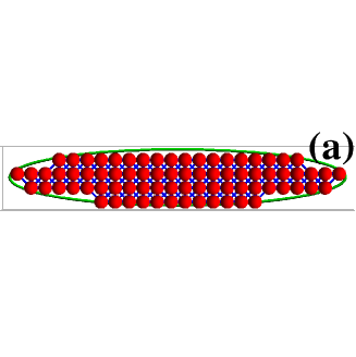
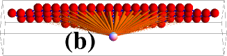
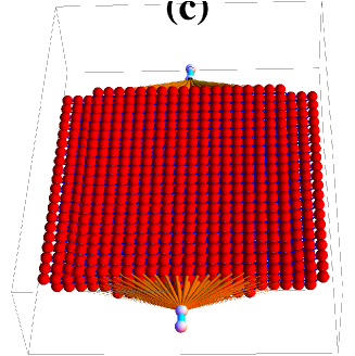
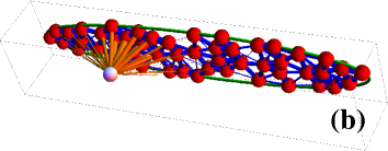
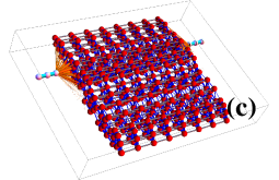
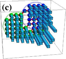
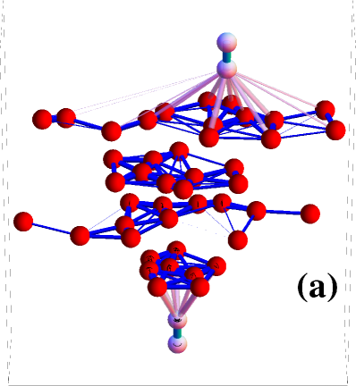
A simple example of a weighted undirected graph associated with a physically realizable nanodevice that may be made into a quantum dragon is shown in Fig. 1. A simple-cubic (SC) lattice structure is presented in Fig. 1. The metal polonium (Po) has a simple cubic lattice structure, and hence Fig. 1 can be viewed as a nano-crystal of Po. Fig. 1(a) shows a single slice of the nanodevice, made up of all atomic sites in a square lattice that fit into a given ellipse. The center of the ellipse is randomly given within a square lattice unit cell, leading to a fixed arbitrary non-isotropic atomic arrangement. The first slice of the nanodevice is connected to the input lead (), tuned as shown in Fig. 1(b). The last slice of the nanodevice is connected to the output lead in an identical fashion, namely for all . An example of a twenty slice () nanodevice connected to the leads is shown in Fig. 1(c), one which may be tuned to be a quantum dragon.
We assume that the on-site energy of the semi-infinite leads is zero, thereby setting our zero of energy. We take the hopping parameters between the lead atoms as , thereby setting our energy scale as the strength of the lead-lead hopping term. We take the lattice spacing within the leads to be unity, setting the unit for length. With these units, only electrons with energies propagate in the leads QMdragon2014 ; DATTA1995 ; DCA2000 .
For the tight-binding model the hopping parameters are obtained from the kinetic energy terms of the Schrödinger equation DATTA1995 , and therefore must be non-positive. That is the reason for the negative sign in the hopping parameter within the leads. We will take all hopping parameters (, , , and ) to be positive, i.e. the hopping strengths are positive. The required negative signs are put in explicitly, so and .
III TRANSMISSION VIA THE MATRIX METHOD
In order the calculate the transmission of an incoming electron as a function of energy, , the time-independent Schrödinger equation needs to be solved. The matrix method for solving the tight-binding model is used here DCA2000 . This method has been used and published a sufficient number of times that the derivation of the equations QMdragon2014 is not required. Therefore, only the relevant equations are given in order to set the notation QMdragon2014 and give the reader the basics of the matrix method.
The nanodevice is composed of slices. For the first two quantum dragon prescriptions, the slices are identical, each with atoms. The equation to solve for the Schrödinger equation of the device (with vertices) and the semi-infinite leads is infinite. After using an ansatz for the leads, the final matrix equation has a linear dimension QMdragon2014 ; DCA2000 . We assume that only atoms in nearest-neighbor slices interact. Fig. 1 shows an example with and . For slices, the matrix equation to analyze has the form
| (1) |
The definition has been made. The quantity can be viewed as the result of coupling the finite graph associated with the nanodevice to the semi-infinite leads. The zero matrices, , are , and the zero vectors have elements. The inter-slice hopping matrix is and has elements of the inter-slice hopping parameters. For the simplest inter-slice connections, as shown in Fig. 1(c), the inter-slice hopping matrix is given by where is the identity matrix. The vector has as its elements the hopping parameters between the last atom of the input lead and the atoms in the first slice. The vector has as its elements the hopping parameters between the first atom of the output lead and the atoms in the last () slice. The matrix , with the energy of the incoming electron. The matrix has as its diagonal element the on-site energy of the atom (vertex). The off-diagonal element of is the intra-slice hopping term . The matrix is symmetric, since the Schrödinger equation involves a Hamiltonian, and we here restrict ourselves to real values for the on-site energies and all the hopping parameters. In Fig. 1(a) the intra-slice hopping terms are shown as cylinders, with the radius of the cylinder representing the strength of the intra-slice hopping term .
The matrix equation to solve for the transmission is given by (again written for slices)
| (2) |
with the definition QMdragon2014 ; DCA2000 . The wavefunction of slice is given by . For a given energy of the incoming electron, the inverse of the matrix of in Eq. (2) is calculated. This enables one to obtain the wavefunctions , as well as and . Note that these all depend on the energy of the incoming electron. The quantity should not be confused with the hopping parameters in ; unfortunately both are conventionally denoted by a lower case , so the subscript denotes that is for the transmission, not a hopping parameter. The transmission probability of the electron is given by
| (3) |
The reflection probability for an electron is given by . Every electron is either reflected or transmitted, so .
IV PROJECTION MAPPING TECHNIQUE
In order to more easily calculate in Eq. (2) we introduce a transformation matrix , written for ,
| (4) |
with the matrices unitary (i.e. ). Note that (written for )
| (5) |
Form the matrix . In the standard fashion, by matrix multiplication the diagonal matrix blocks in are given by . The non-zero off-diagonal blocks of are given by and , or by the complex congugates. For example, for
| (6) |
Multiplying Eq. (2) on the left by , inserting between and the vector in Eq. (2) that contains the wavefunctions, and using Eq. (5) gives (written for )
| (7) |
We have complete freedom to choose the unitary transformation matrices . Assume we can find a that satisfies the four mapping equations QMdragon2014
| (8) |
| (9) |
| (10) |
and
| (11) |
The matrices and are not important, since they will not be connected by any path to either the input or output leads QMdragon2014 .
Introduce the matrix , written for , as
| (12) |
with . This is the matrix formed from only the transformed-sites in Eq. (7) that are connected to the leads, after the mapping equations Eq. (8) through Eq. (11) are used.
The probability of transmission of the electron of energy , are calculated from found from either the equation (written for , with the displayed vectors of length )
| (13) |
or from the equation (written for , with the displayed vectors of length )
| (14) |
where the are the first element of the vector . The mapping equations of Eq. (8) through (11) thus reduce substantially the size of the matrix that one must find the inverse of in order to calculate . The matrix is while the matrix is . Note that provided the mapping equations [Eq. (8) through (11)] hold, no approximation is made by going from Eq. (13) to Eq. (14), as they both give identical transmissions .
V QUANTUM DRAGONS FROM MAPPING
Recall that our lead sites have on-site energies set to zero and a hopping of strength unity. The nanodevice will be a quantum dragon, i.e. will have , if and . The reason for the complete transmission of electrons of all energies is that these are the values that the matrix in Eq. (12) would have if one used the matrix method to calculate the transmission through a homogeneous infinite wire, but selected a string of lead sites to be a nanodevice. Since the wire is homogeneous, there is no scattering by the nanodevice, and the electrons for any energy that propagate through the lead would be completely transmitted. Note, however, that the original slices (as in Fig. 1) may be very inhomogeneous, which may lead to strong scattering of the electrons.
There is complete freedom in terms of the transformation matrices that are used. The only requirement to go from Eq. (13) to Eq. (14) is that the four mapping equations, Eq. (8) through (11), are satisfied. For the first two quantum dragon prescriptions, only nanodevices with the simplest inter-slice coupling between identical slices (as in Fig. 1(c)) will be analyzed. This means the inter-slice hopping matrix is . Hence Eq. (9) is satisfied since is unitary. Thus one has for these two prescriptions . In order to have the nanodevice have the possibility of being a quantum dragon we tune the parameter . Therefore, for such a quantum dragon nanodevice we need only to find a transformation matrix that satisfies Eqs. (8), (10) and (11), and that have and .
The third quantum dragon prescription will require the four mapping equations, Eqs. (8) through (11) to be satisfied, and to have for each slice the mapped on-site energy , between each nearest-neighbor pair of slices , between the input lead and the first slice , and between the output lead and the last () slice .
VI QUANTUM DRAGONS: PRESCRIPTION 1
We consider a weighted undirected graph made from identical slices each with atoms. As in Fig. 1 the weighted graph may be associated with the tight-binding model on a physical nanodevice. We assume the intra-slice matrix elements are all fixed to arbitrary values (both the on-site energies and intra-slice hopping terms ). We assume that the slice atoms are strongly connected, in the sense of graph theory BUSA1965 ; CHART2012 . In other words, within a slice every atom can be visited starting from any other atom by a series of hops using only the non-zero intra-slice hopping terms . We assume that only the simplest inter-slice connections are present, so . We assume we are free to tune all the lead-slice connection strengths in and , to add a constant electric potential to the on-site energy of every slice (which is the same for every atom in the nanodevice), and to tune the strength of the inter-slice hopping strengths .
Let be the maximum of zero or the largest positive diagonal element of , i.e.
| (15) |
with the the on-site energies, which are the diagonal elements of the matrix . Introduce the matrix
| (16) |
Then the matrix is non-negative MarcusMinc64 ; BermanPlemmons1979 , which is written as . In other words, every element of is positive or zero. Let be the normalized eigenvector of associated with the largest eigenvalue of , i.e.
| (17) |
Since has an associated strongly connected graph and is non-negative, by a well-known extension of the Perron-Frobenius theorem MarcusMinc64 ; BermanPlemmons1979 the vector is unique and can be written with all non-negative values (). Then is also an eigenvector of with eigenvalue , i.e.
| (18) |
Remember that the eigenvalues are functions of all the elements of , including the largest diagonal element of , i.e.
| (19) |
Note that and are symmetric, so that they can be associated with an undirected graph, as opposed to being associated with a directed graph as would be required for general non-negative matrices. Since is symmetric, is both a right and left eigenvector of .
We tune the lead-device hopping terms, which must all be non-positive, to be
| (20) |
with some overall strength that we will determine below. The strengths are the same for the connections to the input and to the output leads. We have had to form the matrix in order to use the Perron-Frobenius theorem to show that one can obtain vectors and with all non-positive values. This is the physical constraint imposed by the hopping being the negative of the kinetic energy portion of the time-independent Schrödinger equation.
Choose the transformation matrix to be (written for )
| (21) |
with orthonormal vectors . The vector is an eigenvector of from Eq. (18). The other vectors for need not be eigenvectors of , only orthonormal to each other and to . With this choice of and , the mapping equation Eq. (10) is satisfied with . Similarly, the mapping equation Eq. (11) is satisfied with . The connections to the input and output leads are the same since all slices are identical.
We tune one parameter by applying a constant electrical potential to every atom in the nanodevice, so the matrix is shifted to the matrix . Note the electric potential shift is the same for all atoms in the nanodevice. Then
| (22) |
With our choice of , the mapping equation Eq. (8) is satisfied with
| (23) |
All four mapping equations have thus been satisfied. For a quantum dragon using this prescription, we need only choose
| (24) |
so that and . We have tuned the lead-slice interactions in , the lead-slice interactions in , the constant shift electrical potential , and the inter-slice hopping strength . In all, we have tuned tight-binding parameters. With the simplest inter-slice connections , the total number of possible parameters in the tight-binding model is equal to
| (25) |
The number of intra-slice hopping terms is , the number of different on-site energies is , the number of lead-slice hopping terms is for the input lead and for the output lead, and there is the inter-slice hopping strength , giving the result in Eq. (25).
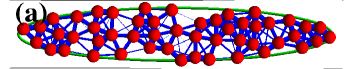
This prescription does not require either that there be any symmetry within a slice or that the underlying graph for a slice is planar. Most importantly, we have not had to tune the connections or the intra-slice hopping strengths in a slice. The slice may be semi-regular, as in Fig. 1, but that is not necessary. One could have each slice, for example, be a portion of a two-dimensional quasi-crystal. One can also have the slices atomic arrangement be completely random, as in an amorphous material. One example of such a complicated, amorphous nanodevice that can be a quantum dragon is shown in Fig. 2. In this prescription, quantum dragons exist everywhere on a dimensional ‘surface’ in the dimensional parameter space.
VII QUANTUM DRAGONS: PRESCRIPTION 2
In the second prescription, we again assume that all slices are identical, and that only the simplest inter-slice hopping is present (). We further assume we have fixed arbitrary lead-device connections , and any fixed arbitrary intra-slice matrix . The subscript stands for the original given problem. We assume every element of is negative, (). We are required to keep fixed the ratios of the elements of , but can tune the overall normalization. Therefore the final lead-site hopping connections are given by
| (26) |
where we can only tune . Similarly, the connection to the output lead is given by
| (27) |
where we can only tune . Choose a coordinate system so the slice-to-slice direction of electron propagation is along the -axis. We assume that the graph associated with is strongly connected, even though may have many elements equal to zero. We further assume we are only allowed to tune the intra-slice matrix by adding an electrical potential at the location of every atom. The electric field is given in the standard fashion, . The electric potential must be continuous, but otherwise its values at points between atoms does not enter the tight binding model. The electric field at the device location is the same for all slices. If atom has the coordinates , the diagonal element of is thus changed by tuning the term . Introduce the diagonal matrix with the diagonal element equal to the tuned electrical potential values, . The new intra-slice matrix with this added electrical potential is
| (28) |
Changing the electrical potential has not changed the intra-slice hopping strengths () or the graph connectivity of a slice.
We choose the electric potential so that , i.e. so all elements of are non-positive. We want to choose a and the diagonal elements of so that
| (29) |
and . Introduce the vector with all elements unity. Since the given has no zero elements, there is a diagonal matrix such that and the inverse (diagonal) matrix exists. Also introduce the square matrix with all elements unity. One has , and for the matrix one has . The diagonal matrix we need to satiisfy Eq. (29) is
| (30) |
where is the Hadamard (element-by-element) matrix product. The proof is that
| (31) |
as required in order to satisfy Eq. (29).
Introduce the magnitude of to be . Now choose the transformation matrix to have the form as in Eq. (21), with , again with orthonormal vectors for . With this choice for the transformation matrix the mapping equation Eq. (10) is satisfied with . Similarly, the mapping equation Eq. (11) is satisfied with . The lead-device connections will allow a quantum dragon if one chooses , which means we need to choose .
We have the simplest possible inter-slice hopping terms, having chosen . As in prescription 1, since the mapping equation Eq. (9) is satisfied. The inter-slice terms allow a quantum dragon if .
With the tuned on-site energies from of Eq. (30), the mapping equation Eq. (8) is satisfied with . We are free to tune , since this would involve an equal shift of the electric potential on every site of the nanodevice. In order to have the intra-slice matrix allow a quantum dragon requires , and therefore we tune to make . From Eq. (30) the required electric potential that must exist at each atomic site is
| (32) |
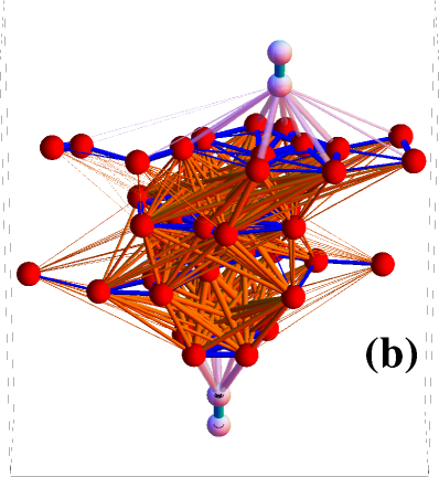
Therefore, we have found the solution to all four mapping equations in order to have a quantum dragon, i.e. to have , for prescription 2. We have tuned tight binding parameters in order to have a quantum dragon, from the total parameters [see Eq (25)]. An example of the tuning of each slice in prescription 2 is illustrated in Fig. 3.
In both prescriptions 1 and 2 the inter-slice mapping equation, Eq. (9), has been satisfied with the inter-slice matrix . However, Eq. (9) could also be satisfied by having an inter-slice matrix of the form
| (33) |
In order to have a quantum dragon from the mapping, Eq. (33) must be satisfied and we must tune the hopping strengths to satisfy . The third prescription is a generalization of this tuning of the inter-slice hopping terms to the case where every slice may be different.
VIII QUANTUM DRAGONS: PRESCRIPTION 3; INHOMOGENEOUS SLICES
We make similar assumptions about the intra-slice interactions as in prescription 1. However, we now let every slice possibly be different. We assume the intra-slice matrices for slices are given fixed values, and all slices are assumed to be strongly connected. We assume we are again allowed to tune a constant electric potential by a constant value for every atom of slice . We assume we are allowed to tune the lead-device connection vector for the input lead, and the lead-device connection vector for the output lead. We further assume that we are allowed to tune every element of the inter-slice hopping matrix for .
For this non-identical slice nanodevice, the matrix equation to analyze has the same form as Eq. (1), with two differences. The diagonal matrices (intra-slice terms) may all be different. The matrices are , where slice has atoms (vertices). The inter-slice terms, may all be different, and are in general not square matrices, being of size . In general, the device-output-lead interaction will usually be tuned to be different from the device-input-lead interaction .
For our non-identical slice case, to perform the mapping the transformation matrix of Eq. (4) will have different unitary transformation matrices of size along the diagonal. The four mapping equations of Eq. (8) through Eq. (11) now become a set of mapping equations. The intra-slice mapping equations are
| (34) |
The inter-slice mapping equations are
| (35) |
The lead-device hopping terms for the input lead must satisfy the mapping equation
| (36) |
while the lead-slice hopping terms for the output lead must satisfy the mapping equation
| (37) |
The matrices and the matrices are not important, since they will not be connected by any path to either the input or output leads QMdragon2014 .
As for Eq. (12), for the non-identical slice case we introduce the matrix , written for , as
| (38) |
with . This is the matrix formed from only the transformed-sites after the mapping equations Eq. (34) through Eq. (37) are used. The probability of transmission of the electron is calculated from the quantities found from the solution of the matrix Eq. (14).
To satisfy the intra-slice mapping equations in Eq. (34), follow the same procedure based on the same arguments as in Eq. (15) to Eq. (24). In particular, introduce the maximum of zero or the largest positive diagonal element of , i.e.
| (39) |
with the the on-site energy of the atom in slice . Introduce the matrix
| (40) |
and hence . Let be the normalized eigenvector of associated with the largest eigenvalue of . Since every has an associated strongly connected graph and is non-negative, by the extension of the Perron-Frobenius theorem MarcusMinc64 ; BermanPlemmons1979 every vector is unique and can be written with all non-negative values (). Hence, is also an eigenvector of with eigenvalue .
We tune the lead-device hopping terms for the incoming lead, which must all be non-positive, to be
| (41) |
with some overall strength . Similarly, we tune the lead-device hopping terms for the outgoing lead, which must be non-positive, to be
| (42) |
with some overall strength . We have thus far had to form the matrices and in order to use the Perron-Frobenius theorem to show the two lead-device vectors and are non-positive, as required for a physical tight-binding model.
Choose the transformation matrices to be (written for )
| (43) |
with orthonormal vectors . The vector is an eigenvector of . The other vectors for need not be eigenvectors of the , only orthonormal to each other and to . With this choice of and the tuned values for the lead-device vectors and , the mapping equations (36) and (37) are satisfied with and .
We apply a constant electrical potential to every atom in the slice of the nanodevice, so every matrix is shifted to the matrix . Then
| (44) |
With our choice of , the mapping equation Eq. (34) is satisfied with
| (45) |
In order to satisfy the mapping equations in Eq. (35) we tune the inter-slice hopping matrices, which are , to be
| (46) |
with arbitrary inter-slice hopping strengths . We have had to form the matrices in order to use the Perron-Frobenius theorem to show that all elements of are non-positive.
All mapping equations for the non-identical slice case have thus been satisfied. For a quantum dragon using this prescription, we need only further tune the values so
| (47) |
so that , , , and for all slices .
Each intra-slice matrix is symmetric, and hence has tight-binding parameters. We have had to tune the diagonal of these by the same amount , so each slice has the one parameter that needs to be tuned. There is only a unique choice for all inter-slice hopping terms and the two lead-slice hopping terms and . The free tight-binding parameters are only from the intra-slice matrices , for a total number of arbitrary parameters
| (48) |
The total number of tight-binding parameters is
| (49) |
An example of the formation of a quantum dragon using prescription 3 is shown in Fig. 4. Prescription 3 does not require any translational symmetry, either along the direction of electron motion in the leads or perpendicular to this axis. Therefore, the nanodevice can be considered to be completely disordered. Nevertheless, all incoming electrons will be completely transmitted through the nanodevice, i.e. it is a quantum dragon having . The quantum dragons exist only on a low-dimensional ‘surface’ [dimension given by Eq. (48)] in the entire tight-binding parameter space [dimension given by Eq. (49)].
IX DISCUSSION AND CONCLUSIONS
We have shown that quantum dragons are ubiquitous. They exist for any fixed atomic bonding arrangement! We have chosen to concentrate on nanodevices with slices, but the prescriptions also work when there is only slice. For , any atomic bonding arrangement between the atoms is possible. The only question in all prescriptions is how many tight-binding parameters need to be tuned, and to what values these parameters must be tuned. The prescribed tight-binding parameters must be tuned in order to satisfy the mapping equations Eq. (8) through Eq. (11). To allow the nanodevice to be a quantum dragon requires further tuning to specific tight-binding values. With careful tuning, electrons of all energies will have complete transmission, , and the device will hence be a quantum dragon.
Three prescriptions, all allowing for quantum dragons from inhomogeneous nanodevices, have been presented in detail. The first two prescriptions have the simplest inter-slice hopping terms, and have every slice identical. The first prescription allows arbitrary fixed values for the positions of all atoms, of all electrical potentials (up to a constant shift), and of all the intra-slice hopping strengths between atoms. In the first prescription the lead-device hopping strengths must be tuned in a prescribed manner in order to obtain a quantum dragon. The second prescription is related to the first, but the lead-device connections are arbitrary values (but identical connections for the input lead and output lead), while the electrical potentials on each atom must be tuned in a prescribed manner in order to obtain a quantum dragon. The third prescription has slices which may all be different, with atomic bonding strengths and electrical potentials (up to a slice-dependent constant term) fixed arbitrarily, while the lead-device and inter-slice hopping terms must be tuned in a prescribed manner in order to obtain a quantum dragon.
For all prescriptions the number of arbitrary parameters is much larger than the number of parameters which must be tuned in a particular fashion. For the first two prescription, the ratio of the number of tight-binding parameters is
| (50) |
where is the number of atoms in every slice of the nanodevice. For the third prescription the number of atoms in each of the slices can be different. However, if all (but the intra-slice bonds and electrical potential may be different for every slice) the ratio of the number of tight-binding parameters is
| (51) |
Thus in all cases, quantum dragons exist only on a low-dimensional ‘surface’ of the high-dimensional tight-binding parameter space. An analogy might be useful to understand the relationship between the complete tight-binding parameter space, the parameter space of the mapping equations, and the parameter space of quantum dragons. Consider a room, so the space has dimension , which can be viewed as the complete parameter space for this analogy. A thin sheet of paper in the room, maybe folded or crumpled, represents the parameter space where the mapping equations hold, here . A curve drawn on the sheet of paper represents the parameter space where quantum dragons exist, here . Clearly, a blind Monte Carlo search of the space would have zero probability of locating a point exactly on the surface, much less on the curve.
The natural question is which, if any, prescription would yield a nanodevice and lead-slice connections that can be realized reasonably easily experimentally. The answer is that all three prescriptions have experimental difficulties. The first prescription can be used to have a single-slice () nanodevice, and a quantum dragon can always be found with the correct lead-device connections. However, to make the lead-slice connections would be physically impossible at the nanoscale, particularly for a non-planar arrangement of atoms in the slice. The second prescription for completely arbitrary lead-device connections would require electric fields on the order of V/m precisely tuned at the nanoscale level. Although not physically impossible, such high electric fields tuned to the nanoscale level would set an extremely high experimental bar. The third prescription requires inter-slice connections that seem impossible, even for the case of Fig. 4 with only about ten atoms per slice.
A more realistic method of experimentally constructing an inhomogeneous quantum dragon might take an approach that is a combination of the three prescriptions. For example, one could require that the lead-device interactions should be monotonically dependent on the distance from the lead atom, and the electric field required to change by no more than a few percent on the nanoscale level. These types of smoothness constraints are not necessary mathematically, but will be critical to synthesizing an experimental realization of inhomogeneous quantum dragons. With such smoothness constraints, a physical nanodevice may be synthesized experimentally using a combination of the first two prescriptions.
The structure of the nanodevice in Fig. 1 in particular seems like this type of quantum dragon should be amenable to experimental synthesis. The metal polonium (Po) has a simple cubic lattice structure, and hence Fig. 1 can be viewed as a nano-crystal of Po. Furthermore, the proofs show that any nano-crystal of Po can be connected to be a quantum dragon, particularly with the end slices as (100) faces as in Fig. 1. Of course, given the half-life of 208Po is about 2.9 y and that of 209Po is about 125 y, a perfect nano-crystal of Po will only survive so long before nuclear decay creates defects. It should be possible to connect homogeneous leads to a Po nano-crystal, and the search for electrical conductivity showing dragon segments may be helped by shaped electric potentials in the nanocrystal.
The proofs of existence of quantum dragon segements here are only for leads of a single channel, and for homogeneous leads. Furthermore, the proofs are for the single-band tight binding model. It may be possible to extend these proofs to multi-channel leads, to other more complicated leads, and to more realistic band models. Of particular interest would be to try to find quantum dragons in face-centered cubic single crystal nanodevices. This paper has shown how ubiquitous quantum dragons are for the simplest cases, but lends hope to their existence in more complicated nanodevices connected to more complicated leads.
It is anticipated that quantum dragons will at least have similar technological applications as do ballistic electron propagation devices Hanson2008 ; Javey2003 ; Wu2012 ; Kim2014 . Previously all known electron propagation with complete electron transmission, , were for homogeneous nanodevices. Whether quantum dragons that are inhomogeneous will enable additional technological applications is an active topic of research.
Acknowledgements Useful conversations are acknowledged with O. Abdurazakov, H. De. Raedt, G. Inkoom, F. Jin, Z. Li, K. Michielsen, T. Neuhaus, P.A. Rikvold, and L. Solomon. Supported in part by US National Science Foundation grant DMR-1206233. Hospitality of the Jülich Supercomputing Centre (JSC) in Jülich, Germany is gratefully acknowledged.
Appendix
Herein details describing the four figures are given. Although the figures are somewhat schematic, being only four examples of quantum dragons, it is informative nevertheless to give details of their construction. The length units are relative since the figures are schematic, but due to the atomic nature of the nanodevice, are expected to be about a nanometer. All figures were made in Mathematica Mathematica .
Figure 1. Fig. 1 shows the construction of a quantum dragon nanodevice using prescription 1 for a nano-crystal cut from a simple cubic lattice. The slice in Fig. 1(a) is made by keeping only sites from a square lattice within an ellipse (green). The square lattice has lattice spacing unity, and each atom is a (red) sphere of radius 0.5. Both nearest-neighbor (which cannot be seen because the spheres touch) and next-nearest hopping terms (blue cylinders) are present. Only the atoms within an ellipse centered at the randomly chosen point with axis along of length 12 and along of length 2 are used in the slice. The number of non-zero hopping terms (number of bonds) in the slice is 236. Fig. 1(b) shows the connections between the lead (white sphere) and the first slice of the nanodevice, with the slice being identical to that of Fig. 1(a). The radius of the lead-device (orange) cylinders are proportional to the strength of a particular lead-device hopping strength . The lead-device hopping values are found by finding a vector which is an eigenvector of with all non-positive elements, which is guaranteed to exist by the Perron-Frobenius theorem. The input lead atom is placed at the CM given by the , but positioned above the first slice. Fig. 1(c) shows the completed nanodevice. Only two atoms (white spheres) in each semi-infinite lead are shown, and for clarity the lead bonds (cyan cylinders) are plotted at a distance of 1.5. The end atom of each semi-infinite lead is plotted to be separated from the blob by 1.5. There are slices plotted, separated by a distance of 1.1. In Fig. 1, since , quantum dragon segments exist on a 154-dimensional ‘surface’ in 3079-dimensional space of all tight-binding parameters.
Figure 2. Fig. 2 shows the construction of a quantum dragon nanodevice using prescription 1 for a randomly constructed slice. (a) The arrangement of the atoms (red spheres) in the slice is constructed by choosing an ellipse (green curve) centered at the origin with an -axis equal to 12 and a -axis equal to 2. Fifty atoms are placed with uniform probability within the ellipse. The atoms are assumed to have a hard radius equal to 0.5, and hence cannot be placed closer than a center-to-center distance of . The intra-slice bonds are shown by (blue) cylinders, with bonds placed between any atoms with . The strength of the intra-slice bonds are given by a linear relationship in the center-to-center distance, with bond strength unity for and zero for . (b) The connection of a slice to a lead atom (white sphere) in order to satisfy prescription 1 is shown. The lead-device hopping strengths are calculated by finding a vector which is an eigenvector of the intra-slice with all non-positive elements. The vector is unique and guaranteed to exist by the Perron-Frobenius theorem. The strength of the lead-slice bonds are proportional to the radii of the (orange) cylinders. The input lead atom is positioned at the CM given by the hopping parameters , but above the plane of the first slice. (c) The complete nanodevice, here composed of identical slices. The transmission can be calculated either from Eq. (13) which requires finding the inverse of a matrix or from Eq. (14) which requires finding the inverse of a matrix. Fig. 2 has , dragon segments exist on a 102-dimensional ‘surface’ in the 1376-dimensional space of all tight-binding parameters.
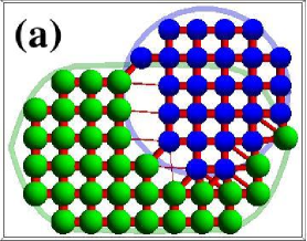
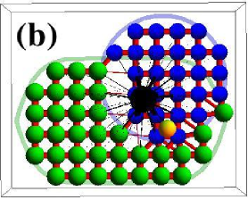
Figure 3. Fig. 3 shows the construction of a slice of a quantum dragon nanodevice using prescription 2. The lattice spacing is set to one for both the green and blue square lattices. (a) The (green sphere) atoms are within a generalized ellipse with the equation
| (52) |
with the center randomly set. All 34 (green) atoms are inside this (green) generalized ellipse but not inside the blue circle of radius 3 centered at the point . The 26 (blue) atoms are inside this (blue) circle. The square lattice of these (blue) atoms is randomly offset from the center. Any of the (blue) atoms inside the circle that would be at a distance less than unity to a (green) atom are not included. The slice has atoms. Green-to-green atom bonds (50 bonds) and blue-to-blue atom bonds (40 bonds) are only between atoms at a distance of unity (nearest neighbors). Green-to-blue atoms bonds are inversely proportional to their length, and are between the atoms at a distance of less than two, giving 26 such bonds. Therefore there is a total of 116 intra-slice bonds (orange cylinders). (b) The yellow sphere shows the position of the lead atom in order for it to be at the center of mass [located at (2.08, -0.33)] of the slice for the eigenvector of (as in prescription 1). Instead, the lead atom is chosen to be at the point (1,1,2), given by the (black) sphere, while the slice is in the plane . Every atom in the slice is connected to the lead atom with a strength (black cylinders) chosen to be proportional to , with the distance between the lead atom and the atom in the slice. (c) The required electric potential at every atom site in the slice is shown (cyan cuboid) in order to make the slice satisfy the mapping of Eq. (8). For visual reasons, these potentials are all shifted by the same amount in order to make them all non-negative. For a quantum dragon, typically the required may be of different signs for different atoms. In Fig. 3, since , dragons live on a 122-dimensional ‘surface’ in the tight-binding 1951-dimensional space.
Figure 4. Fig. 4 shows the construction of a quantum dragon nanodevice using prescription 3 for completely random inhomogeneous slices. The figure has slices. The ellipse for the random placement of atoms in each slice has the in Table 1 and . The spheres have a hard core radius , and the intra-slice bonds are for any atom pairs in the same slice with a distance less than . Table 1 shows the specific values for each slice. The fixed intra-slice bond strengths are proportional to the width of the intra-slice (blue) cylinders, and were chosen as a linear function of distance, with width one for and width zero for . The diameters of the cylinders of the inter-slice bonds, and of the lead-device bonds, are proportional to the tuned bond strengths required for the device to be a quantum dragon. The input (output) lead atoms are placed at the CM of the hopping parameters () that connect the input (output) lead to the atoms in the first (last or ) slice, but just below (above) the first (last) slice. In Fig. 4, since and the are listed in Table 1, the quantum dragons exist on a 270-dimensional ‘surface’ in the 652-dimensional space of all tight-binding parameters.
| Slice # | # intra-slice | ||
|---|---|---|---|
| bonds | |||
| 1 | 8 | 2.0 | 28 |
| 2 | 12 | 8.0 | 27 |
| 3 | 10 | 4.0 | 33 |
| 4 | 14 | 10.0 | 38 |
References
References
- (1) M.A. Novotny, “Energy-independent total quantum transmission of electrons through nanodevices with correlated disorder”, Phys. Rev. B 90, 165103 [14 pages] (2014)
- (2) R. Landauer, “Spatial variation of currents and fields due to localized scatters in metallic conduction”, IBM J. Research and Development 1, 223-231 (1957).
- (3) S. Datta, Electronic Transport in Mesoscopic Systems (Cambridge University Press, Cambridge, UK, 1995).
- (4) D.K. Ferry and S.M. Goodnick, Transport in Nanostructures (Cambridge University Press, Cambridge, UK, 1997).
- (5) S. Datta, Quantum Transport: Atom to Transistor (Cambridge University Press, Cambridge, UK, 2005).
- (6) G.W. Hanson, Fundamentals of Nanoelectronics, (Prentice-Hall, Englewood Cliffs, NJ, 2008).
- (7) Y.V. Nazarov and Y.M. Blanter, Quantum Transport (Cambridge University Press, Cambridge, UK, 2009).
- (8) H.-S. Wong and D. Akinwande, Carbon Nanotube and Graphene Device Physics (Cambridge University Press, Cambridge, UK, 2011).
- (9) Shankar R., Principles of Quantum Mechanics, Second Edition (Plenum Press, London, 1994).
- (10) J.W. Mintmire, B.I. Dunlap, and C.T. White, “Are fullerene tubules metallic?”, Phys. Rev. Lett. 68, 631-634 (1992).
- (11) N. Hamada, S.I. Sawada, and A. Oshiyama, “New one-dimensional conductors: Graphitic microtubules”, Phys. Rev. Lett. 68, 1579-1581 (1992).
- (12) S. Frank, P. Poncharal, Z.L. Wang, and W.A. de Heer, “Carbon nanotube quantum resistors”, Science 280, 1744-1746 (1998).
- (13) M.S. Dresselhaus, G. Dresselhaus, J.C. Charlier, and E. Hernández, “Electronic, thermal and mechanical properties of carbon nanotubes”, Phil. Trans. R. Soc. Lond. A 362, 2065-2098 (2004).
- (14) S.J. Tans, M.H. Devoret, H. Dai, A. Thess, R.E. Smalley, L.J. Geerligs, and C. Dekker, “Individual single-wall cargon nanotubes as quantum wires”, Nature 386, 474-477 (1997).
- (15) C. Berger, Y. Yi, Z.L. Wang, and W.A. de Heer, “Multiwalled carbon nanotubes are ballistic conductors at room temperature”, Appl. Phys. A 74, 363-365 (2002).
- (16) D. Daboul, I. Chang, and A. Aharony, “Series expansion study of quantum percolation on the square lattice”, Euro. J. Phys. B 16, 303-316 (2000).
- (17) M.F. Islam and H. Nakanishi, “Localization-delocalization transition in a two-dimensional quantum percolation”, Phys. Rev. E 77, 061109 [9 pages] (2008).
- (18) E. Cuansing and J.-S. Wang, “Quantum transport in honeycomb lattice ribbons with armchair and zigzag edges coupled to semi-infinite linear chain leads”, Euro. Phys. J. B 69, 505-513 (2009).
- (19) S. Boettcher, C. Varghese, and M.A. Novotny, “Quantum transport through hierarchical structures”, Phys. Rev. E 83, 041106 [12 pages] (2011).
- (20) Z. Lin and Y. Liu, “Electronic transport properties of the Bethe lattices”, Phys. Lett. A 320, 70-80 (2003).
- (21) C. Varghese and M.A. Novotny, “Quantum transport through fully connected Bethe lattices”, Inter. J. Mod. Phys. C 23, 1240010 [10 pages] (2012).
- (22) R.G. Busacker and T.L. Saaty, Finite Graphs and Networks: An Introduction with Application (McGraw-Hill, New York, 1965).
- (23) G. Chartrand and P. Zhang, A First Course in Graph Theory (Dover Publications, New York, 2012).
- (24) M. Marcus and H. Minc, Matrix Theory and Matrix Inequalities (Dover Scientific, New York, 1992) from the 1964 original edition.
- (25) A. Berman and R.J. Plemmons, Nonnegative Matrices in the Mathematical Sciences (Academic Press, New York, 1979).
- (26) A. Javey, J. Guo, Q. Wang, M. Lundstrom, and H. Dai, “Ballistic carbon nanotube field effect transistors”, Nature 424, 654-657 (2003).
- (27) J. Wu, L. Xie, G. Hong, H. En Lim, B. Thendie, Y. Miyata, H. Shinohara, and H. Dai, “Short channel field-effect transistors from highly enriched semiconducting carbon nanotubes”, Nano Research 5, 388-394 (2012).
- (28) S.H. Kim, W. Song, M.W. Jung, M-A. Kang, K. Kim, S-J. Chang, S.S. Lee, J. Lim, J. Hwang, S. Myung, and K-S. An, “Carbon nanotube and graphene hybrid thin film for transparent electrodes and field effect transistors”, Adv. Mater. 26, 4247-4252 (2014).
- (29) Wolfram Research, Inc., Mathematica, Version 9.0, Champaign, IL (2012).