Measuring the magnetic moment density in patterned ultrathin ferromagnets
with submicron resolution
Abstract
We present a new approach to infer the surface density of magnetic moments in ultrathin ferromagnetic films with perpendicular anisotropy. It relies on quantitative stray field measurements with an atomic-size magnetometer based on the nitrogen-vacancy center in diamond. The method is applied to microstructures patterned in a 1-nm-thick film of CoFeB. We report measurements of with a few percent uncertainty and a spatial resolution in the range of nm)2, an improvement by several orders of magnitude over existing methods. As an example of application, we measure the modifications of induced by local irradiation with He+ ions in an ultrathin ferromagnetic wire. This method offers a new route to study variations of magnetic properties at the nanoscale.
Ultrathin ferromagnetic films with perpendicular magnetic anisotropy (PMA) have attracted considerable interest over the last years both for fundamental studies in nanomagnetism and for the development of a new generation of low power spintronic devices Ikeda2010 ; Parkin2008 ; Thiaville2012 . In this context, it is crucial to determine accurately the surface density of magnetic moments in such ultrathin ferromagnets, which can not be simply inferred from tabulated bulk values owing to significant interface effects Ryu2014 . To this end, macroscopic magnetometry methods like superconducting quantum interference devices (SQUIDs) or vibrating-sample magnetometers have become ubiquitous owing to simplicity of use. However, these conventional techniques are prone to parasitic magnetic signals, leading to an intrinsic background on the order of A.m2 Ney2008 ; Garcia2009 ; Pereira2011 , which corresponds to Note . To overcome this background, the ferromagnetic signal needs to be averaged over a large sample, thus limiting drastically the spatial resolution of the measurement. As an example, we consider a ferromagnetic film with a typical thickness nm and a saturation magnetization of A/m, corresponding to a surface density of magnetic moments . In order to reach a signal-to-background ratio of , the signal must be averaged over a surface larger than .
Different approaches have been used to tackle this issue. Notably, a recent improvement of the spatial resolution down to the order of has been achieved by measuring the dipolar repulsion of magnetic domain walls with a magneto-optical Kerr microscope Vernier2014 . The use of micro- and even nano-SQUID also allows for a significant gain in sensitivity and resolution. However it remains difficult with such devices to determine accurately the link between magnetic flux and magnetization, and thus to extract precise values of Wernsdorfer2009 .
In this work, we use a single nitrogen-vacancy (NV) center in diamond as an atomic-size magnetometer to probe the stray field above ultrathin ferromagnets and infer on a scale smaller than . Importantly, the experiment operates under ambient conditions without applying any external magnetic field, which enables excluding parasitic signals from extrinsic magnetic impurities. As an example of application, we demonstrate how this method can be used to study local variations of magnetic properties with submicron resolution, by measuring modifications of induced by local irradiation with He+ ions in an ultrathin ferromagnetic wire.
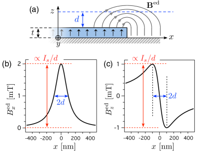
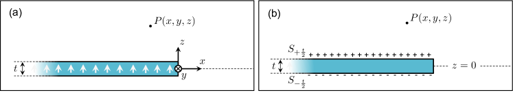
We start by describing the general principle of the method. Any magnetization pattern presenting a non-zero divergence produces magnetic charges with opposite signs, which play a role similar to electric charges in electrostatics. Therefore, a magnetic film with PMA can be seen as the magnetic counterpart of a planar capacitor. In a same way that an electric field is only generated out of the edges of a planar capacitor, magnetic field is only produced at the edge of an uniformly magnetized ferromagnetic film. The central idea of this work is to directly infer the surface density of magnetic moments through local and quantitative measurements of this stray field, denoted . For an ultrathin magnetic film with PMA, it scales linearly with the number of surrounding magnetic moments and can be computed analytically at any distance above the edge. In the limit and considering a one-dimensional (1D) model with an infinitely long edge along the axis [Fig. 6(a)], the stray field components above an edge placed at are simply given by SI
| (1) |
For both components, the field maximum scales as while the characteristic width of the distribution is given by [see Figs. 6(b) and (c)]. The value of and can therefore be directly inferred by using Eq. (4) to fit magnetic field distributions recorded above the edge of an uniformly magnetized ferromagnetic film.
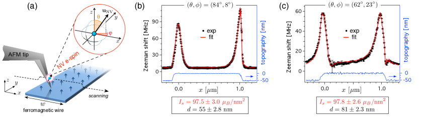
Although the principle of the method is rather simple, its experimental realization is highly demanding since it requires quantitative magnetic field measurements combined with a spatial resolution at the nanoscale. To meet these requirements, we employ a recently introduced magnetometry technique based on a single NV defect in diamond Taylor2008 ; Balasubramanian2008 ; Rondin2012 . This point-like impurity has a spin triplet ground state whose electron spin resonance (ESR) can be interrogated by optical means Gruber_Science1997 . This property enables quantitative magnetic field measurements within an atomic-size detection volume by recording Zeeman shifts of the NV defect electronic spin sublevels Rondin2014 . In the last years, NV-based magnetometry has been used to investigate magnetic vortices Rondin2013 and spin-wave excitations in ferromagnetic microdiscs Yacoby2014 , as well as domain walls in ultrathin ferromagnets Tetienne2014 and bio-magnetism LeSage2013 . In the present study, a single NV defect hosted in a diamond nanocrystal is grafted at the apex of an atomic force microscope (AFM) tip and scanned across the edge of an uniformly magnetized ferromagnetic film [Fig. 2(a)]. At each point of the scan, the stray field is encoded into a Zeeman shift of the NV defect ESR frequency, which is well approximated by in the magnetic field range considered in this work ( mT) Rondin2014 . Here is the transverse zero-field splitting parameter of the NV sensor which is typically on the order of few MHz, GHz/T is the electronic spin gyromagnetic ratio and is the magnetic field projection along the NV defect quantization axis , defined by the spherical angles in the laboratory frame of reference [Fig. 2(a)]. These angles are measured independently by recording the ESR frequency as a function of the amplitude and orientation of a calibrated magnetic field while the parameter is precisely inferred by recording an ESR spectrum in zero field Rondin2013 .
As a first experiment, scanning-NV magnetometry was used to infer the magnetic moment density in a 1-nm-thick film of CoFeB with PMA. More precisely, we studied a multilayer stack of Ta(5 nm)|CoFeB (1 nm)|MgO(2 nm)|Ta(5 nm) deposited by sputtering on a Si/SiO2 substrate SI ; Burrowes2013 . The film was patterned into 1-m-wide magnetic wires using e-beam lithography followed by ion beam etching. The stray field across the magnetic wire then reads
| (2) |
where the field components of are given by Eq. (4) and is the wire width [Fig. 2(a)]. Using a wire rather than a single edge provides a more reliable distance reference along the axis, which enables us to correct any systematic error caused by the calibration of the AFM scanner. A typical Zeeman-shift profile recorded while scanning the NV defect through the edges of the wire is shown in Fig. 2(b) together with the simultaneously recorded topography of the sample. Here the Zeeman shift results from the projection of along the NV axis. Using a NV probe with a different orientation therefore leads to a modified Zeeman-shift profile, as illustrated in Fig. 2(c). We note that the dissymmetry between the field maxima above the two edges is linked to the topography of the sample and the precise position of the NV defect with respect to the end of the AFM tip SI .

The experimental data were then fitted to Eq. (2) with and as free parameters, while taking into account the topography of the sample SI . The results of the fit are indicated as red solid lines in Figs. 2(b) and (c), showing a very good agreement with experimental data. To analyze the precision of the fitting procedure, a statistic of the fit outcomes () was obtained for each NV probe by fitting a set of independent measurements, leading to a standard deviation smaller than . Uncertainties induced by those on the NV defects characteristics and the magnetic wire geometry were carefully analyzed by following the method described in detail in Ref. Tetienne2014bis . This leads to an overall uncertainty of the fit outcomes () on the order of a few percents. We stress that experiments performed with different NV probes yield to identical results for , which further illustrates the robustness of the method [Figs. 2(b),(c)]. For a 1-nm-thick film of CoFeB with PMA, we obtain . This value is in good agreement with measurements performed on the same films with conventional SQUID magnetometry Vernier2014 .
The main advantage of our approach over existing methods is the large gain in spatial resolution. Indeed, by probing the field in close vicinity of the sample, quantitative values of can be obtained locally as long as the field maxima above the edges can be spatially resolved. As shown in Fig. 6, the lateral spread of the stray field is on the order of . The further the probe, the wider the field features, which is clearly visible in Figs. 2 (b) and (c). The spatial resolution of measurement is therefore on the order of , which is the range of - nm in this work. This corresponds to an improvement by at least four orders of magnitude over other existing methods Vernier2014 . We note that in the present work the probe-to-sample distance is limited by (i) the size of the diamond nanocrystal ( nm) and (ii) its imperfect positioning at the apex of the AFM tip Tetienne2013 . Further improvement of the spatial resolution down to nm could be achieved by employing a single NV defect hosted in all-diamond scanning probe tips Maletinsky2012 .
Local determination of through stray field mapping is not limited to magnetic samples with a 1D geometry, like a wire. The method can be easily extended to any type of nanostructured sample. This is illustrated by measuring the magnetic moment density of a 2D structure consisting of a -nm-wide square dot etched in a Ta|CoFeB (1 nm)|MgO film [Fig. 3(a)]. The full Zeeman-shift distribution recorded above the square dot with a scanning-NV magnetometer is shown in Fig. 3(b). By fitting Zeeman-shift linecuts across the square, we infer once again . Using this value, the full distribution was computed showing an excellent agreement with the experiment [Fig. 3(d)].
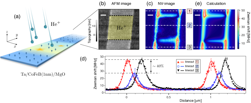
As a last experiment, we demonstrate how stray field imaging with scanning-NV magnetometry can be used as an efficient tool to analyze the uniformity of in ultrathin ferromagnets with submicron resolution. To this end, we investigate local modifications of induced by light irradiation with He+ ions [Fig. 4(a)]. This method enables precise tuning of PMA and magnetization through intermixing at both Ta|CoFeB and CoFeB|MgO interfaces, and can be adjusted by varying the irradiation dose Chappert1998 ; Devolder2013 . A 1-m-wide wire of Ta|CoFeB (1 nm)|MgO was irradiated through a mask with He+ ions at keV energy with a fluence of ions/cm2 SI . An AFM image of the sample indicating the irradiated area is given in Fig. 4(b), while the corresponding Zeeman-shift distribution recorded with scanning-NV magnetometry is shown in Fig. 4(c). Two important features can be observed. First, a stray field is generated at the border of the irradiated window along the long axis () of the wire. This indicates an abrupt variation of induced by local irradiation. Second, the stray field at the edge of the wire is significantly lower in the irradiated region, corresponding to an overall decrease of . To get more quantitative information, Zeeman-shift linecuts were extracted from the image [Fig. 4(d)]. By fitting the data, we infer a relative decrease of by in the irradiated area. We stress that for this particular experiment the exact knowledge of either or is not even required to infer the relative variation of , since it is directly given by the ratio between the field maxima above the edge of the wire. The full Zeeman-shift distribution calculated with the parameters inferred from the fit reproduces very well all the characteristic features of the measurement [Fig. 4(e)]. From this experiment, we can conclude that the irradiation process uniformly modifies the magnetic properties, at least on a length scale of nm corresponding to the spatial resolution of our measurement.
In conclusion, we have introduced a novel approach based on quantitative magnetic field imaging to infer locally and in a very sensitive fashion the magnetic moment density in ultrathin films with PMA. By employing a scanning-NV magnetometer, this method leads to absolute measurements of with a few percent uncertainty combined with a spatial resolution below nm)2. This corresponds to an improvement by more than four orders of magnitude compared to state-of-the-art techniques Vernier2014 . The principle of the method being quite general, it could be extended to any kind of magnetization pattern by merely computing different equations used for data fitting. This method opens new perspectives for studying variations of magnetic properties at the nanoscale.
The authors thank L. Rondin, J.-V. Kim, S. Rohart, A. Thiaville, T. Devolder, S. Eimer and L. Herrera Diez for experimental assistance and fruitful discussions. This research has been partially funded by the European Community’s Seventh Framework Programme (FP7/2007-2013) under Grant Agreement n∘ 611143 (Diadems) and n∘ 257707 (Magwire), by C’Nano Ile-de-France through the project Nanomag, by the RTRA Triangle de la Physique and by the Labex NanoSaclay through the project Siltene.
References
- (1) S. Ikeda, K. Miura, H. Yamamoto, K. Mizunuma, H. D. Gan, M. Endo, S. Kanai, J. Hayakawa, F. Matsukura, and H. Ohno, A perpendicular-anisotropy CoFeB-MgO magnetic tunnel junction, Nat. Mater. 9, 721 (2010).
- (2) S. S. P. Parkin, M. Hayashi, and L. Thomas, Magnetic domain-wall racetrack memory, Science 320, 190 (2008).
- (3) A. Thiaville, S. Rohart, E. Jué, V. Cros, and A. Fert, Dynamics of Dzyaloshinskii domain walls in ultrathin magnetic films, Europhys. Lett. 100, 57002 (2012).
- (4) K.-S. Ryu, S.-H. Yang, L. Thomas, and S. S. P. Parkin, Chiral spin torque arising from proximity-induced magnetization, Nat. Commun. 5, 3910 (2014).
- (5) A. Ney, T. Kammermeier, V. Ney, K. Ollefs, and S. Ye, Limitations of measuring small magnetic signals of samples deposited on a diamagnetic substrate, J. Magn. Magn. Mater. 320, 3341 (2008).
- (6) M. A. Garcia, E. Fernandez Pinel, J. de la Venta, A. Quesada, V. Bouzas, J. F. Fernandez, J. J. Romero, M. S. Martin Gonzalez and J. L. Costa-Krmer, Sources of experimental errors in the observation of nanoscale magnetism, J. Appl. Phys. 105, 013925 (2009).
- (7) L. M. C. Pereira, J. P. Araujo, M. J. Van Bael, K. Temst, A. Vantomme, Practicall limits for detection of ferromagnetism using highly sensitive magnetometry techniques, J. Phys. D: Appl. Phys. 44, 215001 (2011).
- (8) In this work ,we use the Bohr magneton as magnetic unit, A.m2.
- (9) N. Vernier, J.P. Adam, S.Eimer, G. Agnus, T. Devolder, T. Hauet, B. Ockert, D. Ravelosona, Measurement of magnetization using domain compressibility in CoFeB films with perpendicular anisotropy, Appl. Phys. Lett. 104, 122404 (2014).
- (10) W. Wernsdorfer, From micro- to nano-SQUIDs: applications to nanomagnetism, Supercond. Sci. Technol. 22, 064013 (2009).
- (11) See supplemental material for details.
- (12) J. M. Taylor, P. Cappellaro, L. Childress, L. Jiang, D. Budker, P. R. Hemmer, A.Yacoby, R. Walsworth, and M. D. Lukin, High-sensitivity diamond magnetometer with nanoscale resolution, Nat. Phys. 4, 810 (2008).
- (13) G. Balasubramanian, et al., Nanoscale imaging magnetometry with diamond spins under ambiant conditions, Nature 455, 648 (2008).
- (14) L. Rondin, et al., Nanoscale magnetic field mapping with a single spin scanning probe magnetometer, Appl. Phys. Lett. 100, 153118 (2012).
- (15) A. Grber, A. Drabenstedt, C. Tietz, L. Fleury, J. Wrachtrup, and C. von Borczyskowski, Scanning confocal optical microscopy and magnetic resonance on single defect centers, Science 276, 2012 (1997).
- (16) L. Rondin, J.-P. Tetienne, T. Hingant, J.-F. Roch, P. Maletinsky, and V. Jacques, Magnetometry with nitrogen-vacancy defects in diamond, Rep. Prog. Phys. 77, 056503 (2014).
- (17) L. Rondin, J.-P. Tetienne, S. Rohart, A. Thiaville, T. Hingant, P. Spinicelli, J. -F. Roch, and V. Jacques, Stray-field imaging of magnetic vortices with a single diamond spin, Nat. Commun. 4, 2279 (2013).
- (18) T.van der Sar, F. Casola, R. Walsworth, and A. Yacoby, Nanometre-scale probing of spin waves using single electron spins, preprint arXiv:1410.6423.
- (19) J.-P. Tetienne, T. Hingant, J.-V. Kim, L. Herrera Diez, J.-P. Adam, K. Garcia, J.-F. Roch, S. Rohart, A. Thiaville, D. Ravelosona, V. Jacques, Nanoscale imaging and control of domain-wall hopping with a nitrogen-vacancy center microscope, Science 344, 1366 (2014).
- (20) D. Le Sage, K. Arai, D. R. Glenn, S. J. DeVience, L. M. Pham, L. Rahn-Lee, M. D. Lukin, A. Yacoby, A. Komeili, and R. L. Walsworth, Optical magnetic imaging of living cells, Nature 496, 486 (2013).
- (21) C. Burrowes, et al., Low depinning fields in Ta-CoFeB-MgO ultrathin films with perpendicular magnetic anisotropy, Appl. Phys. Lett. 103, 182401 (2013).
- (22) J.-P. Tetienne, et al.,The nature of domain walls in ultrathin ferromagnets revealed by scanning nanomagnetometry, preprint arXiv:1410.1313
- (23) J.-P. Tetienne, T. Hingant, L. Rondin, S. Rohart, A. Thiaville, J.-F. Roch and V. Jacques, Quantitative stray field imaging of a magnetic vortex core, Phys. Rev. B 88, 214408 (2013).
- (24) P. Maletinsky, S. Hong, M. S. Grinolds, B. Hausmann, M. D. Lukin, R. L. Walsworth, M. Loncar, and A. Yacoby, A robust scanning diamond sensor for nanoscale imaging with single nitrogen-vacancy centres, Nat. Nano. 7, 320 (2012).
- (25) C. Chappert,et al., Planer patterned magnetic media obtained by ion irradiation, Science 280, 1919 (1998).
- (26) T. Devolder, I. Barisic, S. Eimer, K. Garcia, J.-P. Adam, B. Ockert, D. Ravelosona, Irradiation-induced tailoring of the magnetism of CoFeB/MgO ultrathin films, J. Appl. Phys. 113, 203912 (2013).
I Supplementary Information
I.1 Samples
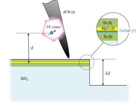
The samples used in this work are stacks of Ta(5)CoFeB(1)MgO(2)Ta(5) deposited on a SiSiO2(100 nm) substrate with a PVD Tamaris deposition tool by Singulus Tech (the number in brackets refers to the layer’s thickness, expressed in nanometers). The stoichiometric composition of the as-deposited CoFeB layer is Co20Fe60B20 for the data of Figs. 2 and 3, and Co40Fe40B20 for the data of Fig. 4. The samples were patterned by e-beam lithography and ion milling to define magnetic wires (for Figs. 2 and 4) or dots (for Fig. 3). The etching depth , comprised typically between 10 and 50 nm, is larger than the depth of the ferromagnetic layer (7 nm), as illustrated in Fig. 5. Finally, a 100-nm-thick gold stripe was defined using a second step of lithography. This stripe is connected to a microwave generator and serves as an antenna to excite the NV center’s spin resonances. Details about the scanning-NV magnetometry setup can be found in Ref. [Rondin2013, ]
For the experiment described in Fig. 4, the sample was annealed at 300∘C for 2 hours, and a third step of e-beam lithography was used to open 1-m-wide windows in a 400-nm-thick PMMA masking layer. The sample was then irradiated with helium ions, with an irradiation dose ions/cm2 and an energy of 15.5 keV, after which the PMMA mask was removed.
I.2 Derivation of the stray field above an edge of a perpendicularly magnetized film
In this section, we derive the stray field above a semi-infinite layer of a ferromagnetic material with perpendicular magnetization. The layer lies in the plane, has a thickness in the direction, and is bounded to the half space, with translation invariance along . The saturation magnetization is denoted .
As shown in Fig. 6, such a magnetic layer may be seen as a capacitance, with magnetic charges on each surface. We can therefore make an analogy with electric field and electric charges. The charges are located on two half planes, one at and one at . We thus start by computing a magnetic potential created at the point by the charge distribution, such that the stray field is defined as the gradient of the potential, . This potential is given by
where is the distance between the point at which we compute the field and a point which belongs to the sample. In the frame of the magnetic layer, with of coordinates it reads
where there is no dependence in due to the translation symmetry.
The integration over gives
while the integration over gives eventually
Finally, we obtain the stray field using the formula , which yields
| (3) |
In the thin-film limit , we can simplify these expressions into
| (4) |
which is Eq. (1) of the main article when the product is replaced by and .
I.3 Fitting procedure
In this section, we describe the fitting procedure used to retrieve the value of in a ferromagnetic wire.
When scanned above a perpendicularly magnetized wire, the NV center feels for each position a field . This field is the contribution from the two edges of the wire and reads in the thin-film approximation
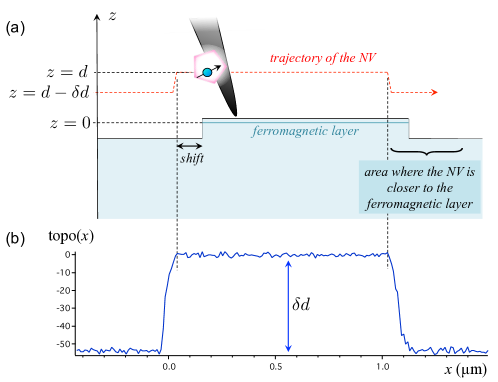
where is defined by Eq. (4), and () is the position of the left (right) edge of the magnetic wire. The height at which the field is probed by the NV depends on position according to the topography followed by the AFM tip, which resembles a top-hat function. The function can be expressed as
where is the average distance between the magnetic layer and the NV center when the AFM tip stands on top of the magnetic wire, and corresponds to the measured topography, with an offset such that
| (5) |
where designates the average over and is the height of the etched wire. As illustrated in Fig. 7a, the functions and may be shifted in with respect to the actual sample’s topography, hence with respect to the magnetic wire, because the NV center may be shifted with respect to the apex of the tip. This is the main reason for the difference in field amplitude associated with the two edges of the wire (see Fig. 2(b) of the main article), since the probe height is in general different for the two edges at and . A typical example of the function extracted from AFM data is shown in Fig. 7b.
Note that since the scanners of our AFM are not equipped with position sensors due to volume constraints, and hence are somewhat imprecise, the topography data together with the Zeeman shift data are first rescaled in order to match the width and height of the magnetic wire as measured by a second, feedback-looped, calibrated AFM.
To obtain a fit function and compare it to experimental data, the magnetic field must be converted into a Zeeman shift of the ESR frequencies of the NV center. Although it is well approximated in the present case by , where is the projection of the magnetic field along the NV axis, we choose here to perform the exact computation by diagonalizing the Hamiltonian of the spin of the NV center
where and are the zero-field splitting parameters of the NV center, is the Planck constant, 28.03(1) GHz/T is the electron gyromagnetic ratio and is the spin operator. The frame is defined by the crystal orientation of the diamond, with being along the axis of the defect, which is characterized by spherical angles in the lab frame [Rondin2013, ; Rondin2014, ].
The resulting theoretical function is finally fitted to the data using least-squares minimization. The fit parameters are the stand-off distance , the magnetic moment density , and the positions and of the two wire’s edges. The other parameters entering the fit function are the NV center’s parameters () used in the Hamiltonian diagonalization, and the geometrical wire’s parameters () used for data rescaling. As mentioned in the main article and explained in details in Ref. [Tetienne2014bis, ], the uncertainties for and are estimated based on the uncertainties of those six independently measured parameters (), as well as on the standard deviation among a series of measurements.
II Summary of the results
The magnetic moment density found for the various samples studied in this work are gathered in Table 1. Note that the value found for the sample irradiated through the PMMA masking layer [Fig. 4 of the main paper] is significantly smaller than the one reported in Ref. [Vernier2014, ] for non-irradiated samples. This is due to the fact that a 400-nm PMMA layer does not completely block 15.5 keV helium ions, as confirmed by SRIM simulation.
| Sample | Co20Fe60B20 | Co40Fe40B20 | Co40Fe40B20 | Co40Fe40B20 |
| as deposited | as deposited | annealed and | annealed and | |
| irradiated | irradiated through | |||
| 400-nm PMMA | ||||
| (/nm2) |