On Resistive Networks of Constant Power Devices ††thanks:
Abstract
This brief examines the behavior of DC circuits comprised of resistively interconnected constant power devices, as may arise in DC microgrids containing micro-sources and constant power loads. We derive a sufficient condition for all operating points of the circuit to lie in a desirable set, where the average nodal voltage level is high and nodal voltages are tightly clustered near one another. Our condition has the elegant physical interpretation that the ratio of resistive losses to total injected power should be small compared to a measure of network heterogeneity, as quantified by a ratio of conductance matrix eigenvalues. Perhaps surprisingly, the interplay between the circuit topology, branch conductances and the constant power devices implicitly defines a nominal voltage level for the circuit, despite the explicit absence of voltage-regulated nodes.
I Introduction
The existence and uniqueness of operating points to nonlinear resistive circuits is a classic topic in circuit theory, with nonlinearities usually entering in the form of voltage or current-controlled nonlinear conductances [1]. Many elegant approaches have been devised to study such nonlinear circuits, from fixed point and global inverse function theorems to the topological concept of the degree of a mapping [2]. These approaches offer a binary answer to the question of operating point existence by inferring existence from continuity and monotonicity, or from sector boundedness conditions on the current-voltage characteristics. These results offer little guidance in estimating the locations of operating points in voltage-space, or in quantifying their behavior as a function of the circuit topology, branch conductances, and loads.
In this brief we consider a modification of classic nonlinear resistive networks, with two distinguishing features. First, the nonlinearities considered herein arise not from nonlinear branch conductances internal to the circuit, but from externally-connected constant-power devices (CPDs). In contrast to conductance models relating branch-wise voltage and current variables, an externally connected CPD constrains the relationship at the connection port between the port voltage and the port current injection . This hyperbolic constraint results in a negative (resp. positive) incremental conductance for sources with (resp. for loads with ), and has been observed to lead to instability in power electronic [3], automotive [4], and power transmission systems [5]. Constant power loads are the most challenging component of the standard ZIP (constant-impedance/current/power) static load model, as their presence often renders analysis and design problems analytically intractable. Second, as a consequence of the CPDs regulating the power sinked or sourced through each port, the circuit lacks voltage-regulated nodes, and therefore lacks a nominal voltage level around which all nodal voltages cluster. For example, in power systems this nominal level is typically supplied by voltage-regulated buses such as generators and points of common coupling [5, 6, 7].
This work is motivated by the increasing deployment of microgrids. These small-footprint power systems offer reliability and flexibility by locally managing generation, storage, and load [8]. While microgrids can be directly connected to a utility, their major benefit comes from the ability to disconnect (or “island”) themselves and operate independently. Resistive circuits with CPDs arise in islanded DC and AC microgrids consisting of constant-power loads (CPLs) and micro-sources [9, 10, 11]. As an example of a micro-source, photovoltaic panels are controlled for maximum power point tracking [12], and appear to the network as constant sources of power. We refer the reader to [8, 9, 10, 11] and the references therein for detailed modeling information on micro-sources and CPLs. Aside from this key application area and circuit-theoretic interest, the proposed analysis and its extensions may prove useful for novel forms of circuit reduction [13], synthesis [7], as a tool for reactive power flow analysis [14, 6], and in power transmission networks when generators reach their capability limits [5].
In Section II we develop the resistive circuit equations, and begin our analysis in Section III by proposing a novels decomposition of the vectorized circuit equation. This decomposition can be thought of as separating the model into two equations: the first describes the resistive losses, while the second describes a complementary “lossless” flow of power. We present a simple and intuitive necessary condition for the existence of operating points. To build intuition for the general analysis which follows, in Section IV we study in detail the simplest CPD circuit consisting of two ports. We provide a necessary and sufficient condition for the existence of an operating point with positive voltages. In Section V we present our main result, partially generalizing the results of Section IV to arbitrary circuit topologies. We present sufficient parametric conditions for all circuit operating points to belong to an appropriately defined operating region, in which the average nodal voltage is high and all voltages are tightly clustered near one another. A loose translation of the condition is the following: the ratio of resistive losses to total transmitted power should be small when compared to the (inverse) network heterogeneity, as quantified by the “eigenratio” [15] of conductance matrix. We regard our analysis as a first step in the theoretical understanding of the operating points of CPD circuits. While intuition suggests that the absence of voltage-regulated nodes will result in the circuit displaying a disorganized voltage profile, our main result shows that the voltage profiles of such circuits are quite uniform under appropriate conditions.
The remainder of this section introduces some notation and preliminaries. Given a vector , is the associated diagonal matrix. The identity matrix is , and (resp. ) is the -dimensional vector of all ones (resp. all zeros). The set is the subspace of all vectors in n orthogonal to . For a vector , , and . For a positive semidefinite symmetric matrix , (the largest eigenvalue), while .
II Derivation of Network Equations

In this paper we consider linear resistive circuits with nodes for a total of nodes. Nodes are the ones of interest, which in our motivating example of a DC microgrid are locations where power will either be produced or consumed. We assume without loss of generality that these nodes form a connected network. For the short transmission lines we consider, the th node (ground) is electrically isolated from the others and taken as the datum. We may therefore consider the circuit as a “grounded -port” where each port voltage is simply the node-to-datum voltage of the respective node [1]. After eliminating any passive internal nodes via Kron reduction [13], the input/output behavior of the -port is described in the short-circuit admittance representation by [1]
| (1) |
where and are the vectors of port currents and voltages, and is the conductance matrix. Each port of our -port is interfaced with a constant power device, which constrains the product of the port current and port voltage to be a constant power . The power injection is positive for generation and negative for load. An -port with CPDs is shown in Figure 1 for a three-port circuit, where only one CPD has been shown. The port constraints due to CPDs read as
| (2) |
where . Substituting (1) into (2), we arrive at our nonlinear network equations
| (3) |
For future use we collect some useful and well-known facts regarding the conductance matrix [1].
Lemma II.1 (Conductance Matrix)
The conductance matrix satisfies the following properties:
-
(i)
is positive semidefinite;
-
(ii)
;
-
(iii)
.
In contrast with nonsingular conductance matrix models derived from reduced node-edge incidence matrices [1] (i.e., incidence matrices in which the row associated to the datum has been removed), the conductance matrix in our port model is singular due to the isolation of the datum node. This can be seen from Figure 1: nodes form a cutset, and hence the net current flow through this cutset — or equivalently, the sum over all port currents — must be zero. In vector notation, this reads as , or using the node equations (1), that . This equality holds for all port voltages if and only if , which is Lemma II.1 (ii). Equivalently, one may consider as the conductance matrix of the sub-network containing all nodes other than the datum.
The second eigenvalue of the conductance matrix is called the algebraic connectivity [16, 17], and measures how strongly connected the circuit is. Similarly, the “eigenratio” quantifies the heterogeneity of the circuit [15]. A large eigenratio corresponds to a heterogeneous and/or weakly connected circuit, while an eigenratio close to unity corresponds to a highly symmetric and dense circuit with nearly uniform conductances.
An operating point is any solution of the circuit equations (3). In contrast to standard circuit problems, the circuit described by (3) has no voltage-regulated sources – all port voltages are free variables. The absence of voltage-regulated sources makes determining the operating points of (3) challenging and non-standard. Intuitively, one might come to the conclusion that the inflexible power demands of the CPDs would conflict with one another, making equilibrium conditions impossible. In the next three sections we develop some basic theoretical results for the circuit model (3) and find that this intuition fails.
III Decomposition of Circuit Equations

The starting point for our analysis of (3) is inspired by the following observations. Under normal conditions, circuits with voltage-regulated nodes (such as power transmission and distribution networks) possess “almost uniform” operating points [6], where all nodal voltages are clustered around a nominal value . We may express this as
| (4) |
where is a nominal voltage level and the vector is a small, dimensionless deviation variable.111Without loss of generality, one may assume that . That is, the voltage profile is the sum of a uniform profile , plus a perturbation term described by . While the solution-space of models such as (3) is generally multi-valued and diverse [18], we nonetheless are interested in such “almost uniform” solutions, as these are the operating points relevant in practice [5]. Lemma II.1 shows that the conductance matrix naturally satisfies a related decomposition, since . Inspired by these properties, we similarly decompose the vector of powers in (3) as
| (5) |
where and . Such a decomposition is uniquely defined, as one may verify by noting that and that , where is the projection matrix onto the subspace . Physically, is the total power dissipated in the network (the net difference between sourced and sinked power), while can be roughly interpreted as the power which flows “losslessly” between nodes. Our first result shows that this change of variables allow us to decompose the power balance (3) into two equations in orthogonal subspaces.
Lemma III.1 (Decomposition)
The voltage vector is an operating point of (3) if and only if
| (6a) | ||||
| (6b) | ||||
Proof.
IV Example: Two Port Circuit
The decomposed circuit equations (6a)–(6b) can be solved in closed form for the specific case of a two port CPD circuit.
Theorem IV.1 (Operating Point for Two Node Circuit)
Consider the circuit (3) defined for two ports connected by a conductance . Then the circuit has a high-voltage operating point with a high average voltage and a small percentage deviation if and only if
| (8) |
If this is condition holds, then the unique operating point is
| (9) |
where
Proof.
Note from the condition (8) that if , then and vice versa. That is, one node must generate power if the other consumes power. Thus, is the absolute sum of power injections/demands at the ports of the network, and the parametric condition (8) admits the elegant physical interpretation that the resistive losses in the network should be small compared to the gross power transferred through the networks ports (Figure 2).
The dependence of both and on the resistive losses is intuitive: as decreases, the deviation vector becomes smaller and the average voltage level rises. That is, the voltage profile becomes increasingly uniform. Conversely, as increases, increases in size linearly, while decreases with the square root of the losses. We invite the reader to compare this result with standard load flow results for networks with fixed-voltage buses [19, Chapter 1]. Unlike the classic results in [19], the existence condition (8) does not depend on the line conductance .
V Sufficient Conditions for General Topologies
We now present sufficient conditions on the circuit parameters of a general -port which guarantee that all operating points of (3) have high average voltage levels and small percentage deviations , generalizing the “small losses relative to total power” intuition developed in Section IV. Unlike Theorem IV.1, we do not provide exact solutions for the circuit operating points, but only bounds for where in voltage-space operating points are located. The results are applicable to general -ports of arbitrary topology.
Theorem V.1 (Operating Regions I)
Theorem V.1 can be understood methodologically as follows. First, using the given data of the problem, compute from the definition in (10). If , then one may compute and from (11a)–(11b), and Theorem V.1 guarantees that all operating points of the circuit will have a high average voltage with minimal deviations . A graphical interpretation of Theorem V.1 for a three-port circuit will be presented later in Section VI. If or , we can make no claims regarding the locations of operating points.
Remark V.2 (Interpretation and Qualitative Behavior)
The parametric condition (10) implies222This follows from the fact that for . that , which may be interpreted as follows: the ratio of resistive losses to total power transmitted must be smaller than the spectral gap of the conductance matrix.
It is useful to compare the sufficient condition (10) to the exact two-port condition (8) in Theorem IV.1 by specializing (10) for a two-port network. In this case it is known that , and the condition (10) reduces to . Thus, compared to (8), the results of Theorem V.1 are more conservative due to the -norm and the factor of . Just as was observed in the two-port case of Theorem IV.1, the variables and are closely related. In the regime of small losses , we observe from (10) that . It follows from (11a)–(11b) that
Thus, the lower bound on the mean voltage level scales with the resistive losses , while the voltage percentage deviations are bounded linearly with . In this regime of low resistive losses, the mean voltage is sensitive to any increase in network losses and will quickly decline, while the percentage deviations will, at most, increase linearly. These observations lead us to conclude that, much like in standard power systems, an accurate balancing of power supply and power demand is crucial to the efficient and stable operation of CPD-dominated DC microgrids.
Proof.
Since for any it holds that , from (6a) we have that
| (12) |
From (6b) it holds that
Taking norms on both sides and bounding, we obtain
| (13) |
where we have used the fact that . Now using the upper bound in (12) and rearranging, (13) becomes
We now calculate using (11b)–(11a) and (12) that
and hence as claimed. ∎
For completeness we present an analogous -norm condition, which similarly restricts the heterogeneity of the network by comparing the smallest branch conductance to twice the largest nodal degree . Depending on the particular topology and heterogeneity of the circuit under consideration, Theorem V.3 may offer more or less conservative results when compared to Theorem V.1.
Theorem V.3 (Operating Regions II)
Consider the circuit equations (3) with the voltage and power decompositions (4)–(5) leading to the decomposed circuit equations (6a)–(6b). Assume that the circuit parameters satisfy
| (14) |
where is the smallest branch conductance, and accordingly define
Then all operating points of the circuit satisfy and .
VI Case Study: Three Node Circuit
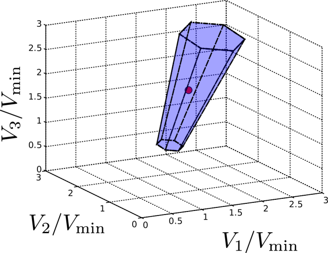
To illustrate and test the results presented in Section V, we consider the network of Figure 1 with parameters kW, kW, S, and S. The (in this case, unique) nonlinear solution to (3) is given by , and hence V and . For these parameters, one calculates using (10) of Theorem V.1 that . The sufficient condition is satisfied, and one readily calculates from (11a) and (11b) that and . The solution space is depicted in Figure 3, which shows that the solution lies inside the set defined in Theorem V.1, as expected. While the bounds developed in Theorem V.1 become increasingly conservative as the number of ports increases, they can be considered as a first step into understanding the fundamental physics of such circuits composed of constant power devices.
VII Conclusions
We have examined the behavior of linear resistive circuits with constant power devices interfaced at the circuit ports, and have provided sufficient conditions on the network parameters for circuit operating points to have high average voltage levels and minimal differences in nodal voltage. A curious observation is that despite the absence of voltage-regulated nodes, the network lower bounds its own mean voltage level, as quantified by (11a).
While we have partially characterized the circuit operating points through bounds, it remains an open question whether the circuit equations (3) are exactly solvable for general topologies, and how the results presented change with full ZIP load models. As an outlook to control applications, the relative scaling of the voltage profile heterogeneity and the minimum average voltage reported in Remark V.2 hint at strategies for voltage profile control in DC microgrids, in which renewable sources are optimized and dispatched to simultaneously adjust the coupled values and .
References
- [1] L. O. Chua, C. A. Desoer, and E. S. Kuh, Linear and Nonlinear Circuits. McGraw-Hill, 1987.
- [2] A. N. Wilson, Nonlinear Networks: Theory and Analysis. IEEE Press, 1975.
- [3] A. M. Rahimi and A. Emadi, “Active damping in DC/DC power electronic converters: A novel method to overcome the problems of constant power loads,” IEEE Transactions on Industrial Electronics, vol. 56, no. 5, pp. 1428–1439, 2009.
- [4] A. Emadi, A. Khaligh, C. H. Rivetta, and G. A. Williamson, “Constant power loads and negative impedance instability in automotive systems: definition, modeling, stability, and control of power electronic converters and motor drives,” IEEE Transactions on Vehicular Technology, vol. 55, no. 4, pp. 1112–1125, 2006.
- [5] I. A. Hiskens, “Analysis tools for power systems — contending with nonlinearities,” Proceedings of the IEEE, vol. 83, no. 11, pp. 1573–1587, 2002.
- [6] B. Gentile, J. W. Simpson-Porco, F. Dörfler, S. Zampieri, and F. Bullo, “On reactive power flow and voltage stability in microgrids,” in American Control Conference, Portland, OR, USA, Jun. 2014, pp. 759–764.
- [7] J. W. Simpson-Porco, F. Dörfler, and F. Bullo, “Voltage stabilization in microgrids via quadratic droop control,” in IEEE Conf. on Decision and Control, Florence, Italy, Dec. 2013, pp. 7582–7589.
- [8] J. M. Guerrero, J. C. Vasquez, J. Matas, L. G. de Vicuna, and M. Castilla, “Hierarchical control of droop-controlled AC and DC microgrids–a general approach toward standardization,” IEEE Transactions on Industrial Electronics, vol. 58, no. 1, pp. 158–172, 2011.
- [9] A. Kwasinski and C. N. Onwuchekwa, “Dynamic behavior and stabilization of DC microgrids with instantaneous constant-power loads,” IEEE Transactions on Power Electronics, vol. 26, no. 3, pp. 822–834, 2011.
- [10] D. Marx, P. Magne, B. Nahid-Mobarakeh, S. Pierfederici, and B. Davat, “Large signal stability analysis tools in DC power systems with constant power loads and variable power loads: A review,” IEEE Transactions on Power Electronics, vol. 27, no. 4, pp. 1773–1787, 2012.
- [11] S. Sanchez, R. Ortega, G. Bergna, M. Molinas, and R. Grino, “Conditions for existence of equilibrium points of systems with constant power loads,” in IEEE Conf. on Decision and Control, Florence, Italy, Dec. 2013, pp. 3641–3646.
- [12] C. Rodriguez and G. Amaratunga, “Analytic solution to the photovoltaic maximum power point problem,” IEEE Transactions on Circuits and Systems I: Regular Papers, vol. 54, no. 9, pp. 2054–2060, 2007.
- [13] F. Dörfler and F. Bullo, “Kron reduction of graphs with applications to electrical networks,” IEEE Transactions on Circuits and Systems I: Regular Papers, vol. 60, no. 1, pp. 150–163, 2013.
- [14] E. C. Furtado, L. A. Aguirre, and L. A. B. Tôrres, “UPS parallel balanced operation without explicit estimation of reactive power – a simpler scheme,” IEEE Transactions on Circuits and Systems II: Express Briefs, vol. 55, no. 10, pp. 1061–1065, 2008.
- [15] A. E. Motter, C. S. Zhou, and J. Kurths, “Enhancing complex-network synchronization,” Europhysics Letters, vol. 69, no. 3, pp. 334–337, 2005.
- [16] M. Fiedler, “Algebraic connectivity of graphs,” Czechoslovak Mathematical Journal, vol. 23, no. 2, pp. 298–305, 1973.
- [17] G. Korniss, M. B. Hastings, K. E. Bassler, M. J. Berryman, B. Kozma, and D. Abbott, “Scaling in small-world resistor networks,” Physics Letters A, vol. 350, no. 5-6, pp. 324–330, 2006.
- [18] G. S. Gajani, A. Brambilla, and A. Premoli, “Numerical determination of possible multiple DC solutions of nonlinear circuits,” IEEE Transactions on Circuits and Systems I: Regular Papers, vol. 55, no. 4, pp. 1074–1083, 2008.
- [19] T. Van Cutsem and C. Vournas, Voltage Stability of Electric Power Systems. Springer, 1998.