Radio-frequency capacitance spectroscopy of metallic nanoparticles
Abstract
Recent years have seen great progress in our understanding of the electronic properties of nanomaterials in which at least one dimension measures less than 100 nm. However, contacting true nanometer scale materials such as individual molecules or nanoparticles remains a challenge as even state-of-the-art nanofabrication techniques such as electron-beam lithography have a resolution of a few nm at best. Here we present a fabrication and measurement technique that allows high sensitivity and high bandwidth readout of discrete quantum states of metallic nanoparticles which does not require nm resolution or precision. This is achieved by coupling the nanoparticles to resonant electrical circuits and measurement of the phase of a reflected radio-frequency signal. This requires only a single tunnel contact to the nanoparticles thus simplifying device fabrication and improving yield and reliability. The technique is demonstrated by measurements on 2.7 nm thiol coated gold nanoparticles which are shown to be in excellent quantitative agreement with theory.
pacs:
73.21.La, 73.63.Kv, 73.23.HkElectrical characterization of metallic nanoparticles using dc transport methods requires both a source and drain electrode to pass a current as well as a gate electrode to vary the chemical potential, see Fig. 1a. The most commonly used fabrication techniques are electromigration, where a metallic wire is controllably loaded to failure such that a nanosize gap opens up in which particles might be trapped, or electrode plating in which a predefined gap is reduced electrochemically Li1 ; Kuemmeth ; Azuma . Although these methods are certainly feasible, the need for two tunnel contacts makes the fabrication complex and challenging and the quality and yield of devices highly variable. This is particularly problematic for the smallest nanoparticles - or molecules - less than around 3 nm in size.
Here we present a different technique that allows the study of arbitrarily small nanoparticles using only a single tunnel contact. Importantly, the technique does not require nm positioning accuracy which facilitates the use of standard lithography methods. As illustrated in Fig. 1b, we achieve this by placing the nanoparticles on a metal electrode and and by capacitively coupling the nanoparticle to a second electrode, which functions both as an ac reference ground and as a dc gate electrode. The devices are embedded in a resonant LC circuit and radio-frequency reflectometry is used as the measurement tool Duty ; Petersson ; Chorley ; Verduijn . This approach, which can be considered as capacitance spectroscopy Ashoori1 ; Ashoori2 taken into the radio-frequency domain, not only simplifies device fabrication but also offers high sensitivity and high bandwidth readout.
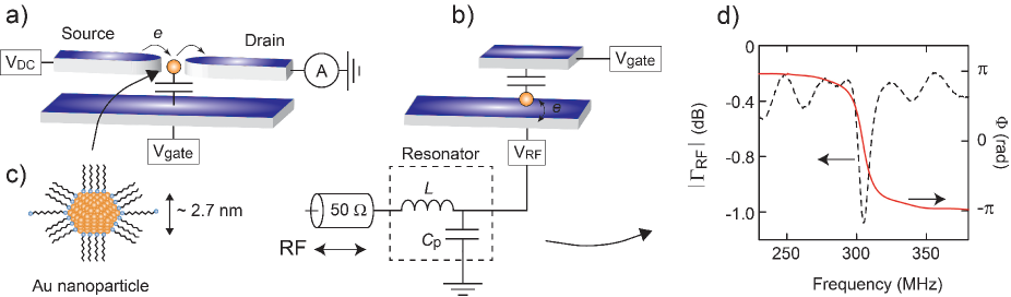
The resonant circuits used in our experiments typically have a resonant frequency in the 300-500 MHz range which is given by the total device capacitance - including parasitics - and a chip inductance placed on the sample holder such that , see Fig. 1d. The key idea is that the capacitance depends in part on the ability of electrons to move on and off the nanoparticle at the driving frequency which in turn depends on the chemical potential of the nanoparticle which can be tuned by the gate electrode. The gate-dependent capacitance is probed by measuring the phase shift of a reflected radio-frequency signal at the resonant frequency .
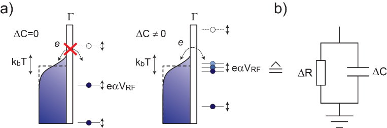
Before discussing experimental data, using Au nanoparticles, we will first examine, quantitatively, the expected phase response of the reflectometry technique for a generic ’electron-in-a-box’ system or quantum dot with discrete energy spectrum, coupled to a metallic lead at some finite temperature , as illustrated in Fig. 2. In the presence of a radio-frequency signal, as in Fig. 1b, the energy levels on the quantum dot will oscillate with respect to the lead. However, it is only possible for electrons to move on and off the quantum dot when an energy level is aligned with the thermally broadened electrochemical potential of the lead. In this case, the occupation probability of the level varies with the drive frequency and the movement of charge on and off the electrode in response to the rf drive amplitude can be parameterized by an effective admittance where is the radial frequency and with capacitance and resistance as shown in Fig. 2b. If the thermal energy is larger than the lifetime broadening of the resonances, , where is the tunnel rate, it is relatively straightforward, see supplementary information, to obtain the following relations using rate equations:
| (1) |
| (2) |
where the term takes into account the position of the discrete energy level with respect to the Fermi level of the lead using a lever arm for conversion from gate voltage to energy Chorley ; Gabelli . If the tunnel rate is comparable to the drive frequency, , dissipation can be significant as previously observed in single-electron tunneling devices Persson ; Ciccarelli . However, if tunnel rates are considerably faster than the drive frequency, that is , the effective resistance diverges and the junction will be capacitive only. It is this limit that we will consider here. Using standard network analysis Pozar , it can be shown, see supplementary information, that in this case the measured phase shift, for an under-coupled resonator, is related to the effective capacitance as:
| (3) |
where is the quality factor of the resonator given by the ratio of the resonant frequency and bandwidth of the resonance. Using the relations 1-3 above we now have the tools to quantitatively investigate single-electron tunneling of any device of nm dimensions in which the energy spectrum is discrete.
Results
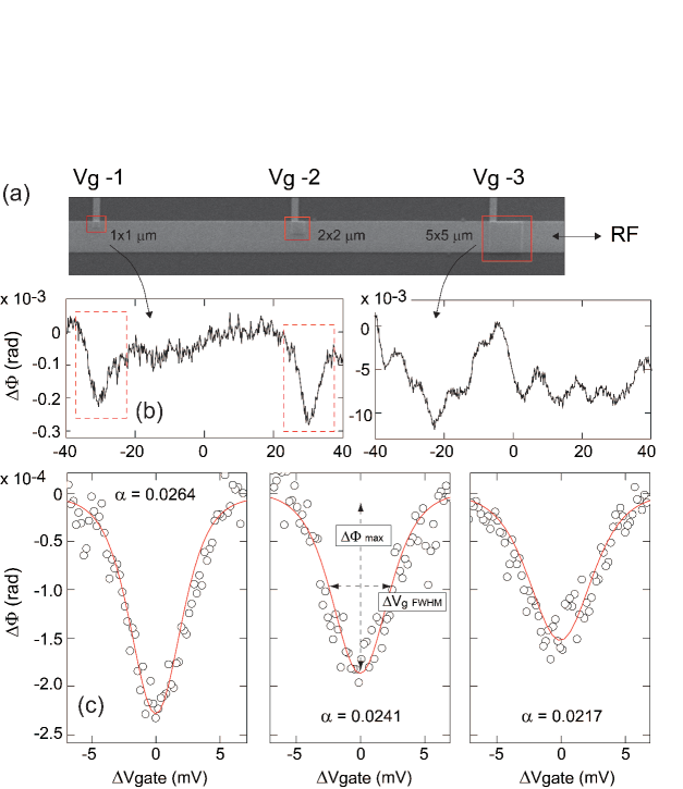
Nanoparticle measurements. To demonstrate the technique experimentally, we have deposited thiol-coated Au nanoparticles of 2.7 nm diameter on a gold substrate. These particles were then covered by approximately 5.5 nm of Al2O3 deposited using atomic layer deposition, see Methods. On top of the oxide layer we defined a set of gate electrodes of varying sizes as illustrated by the scanning electron microscope (SEM) images in Fig. 3a. The results of measurements on two representative structures of different size in a He-3 cryostat with a base temperature of 400 mK are shown in Fig. 3b. The number of particles under the large 5 x 5 m gate electrodes is not exactly known but, given an approximate density of Au nanoparticles of 10-50 m-2, see supplementary information, is likely to be large. Therefore, even though for individual particles the energy levels are expected to be well separated, the measurements on this gate electrode show an interleaving of the signal of many particles, resulting in the oscillatory pattern seen in the right panel image of Fig. 3b. For the measurements shown in the left panel of Fig. 3b, the gate overlap is significantly reduced - by a factor of 25 - and we observe more pronounced dips against a relatively flat background. For these devices the number of nanoparticles under the gate electrodes is sufficiently low for the observation of tunneling through individual electron states as we will examine in more detail. We also performed a series of control experiments, see supplementary information, in which no nanoparticles were deposited and in which we did not see any features in the measurements.
Using the relations 2 and 3 obtained above for versus we are able to compare the experimental data with theory. We obtain an excellent fit for individual resonances, see Fig. 3c, where the only free parameter is the lever arm which sets both the width and depth of the dips. The width of the dips , or, more precisely, the full-width-half-maximum is 3.53 which is identical to what is expected in dc transport of individual quantum states Meirav ; Beenakker ; Foxman . However, unlike dc transport in which the magnitude of the conductance is set by the tunnel rate and asymmetry of the source and drain tunnel junctions, in the reflectometry measurements - in which there is only a single tunnel junction - the magnitude . We thus have two relations for and which can be obtained independently. Indeed, while in our experiments the temperature is known, mK, if the temperature is set as an additional fit parameter, the fit procedure yields the correct experimental result. This enables an energy calibration without the need of a source-drain bias voltage and allows measurements of, for example, the charging energy of the nanoparticles or, when a magnetic field is applied, measurements of the g-factor or energy spectrum Ashoori1 ; Ashoori2 .
Nano-thermometry. A further important consequence is that our devices can be used as a primary thermometer, that is, a thermometer that allows temperature measurements without calibration by another thermometer. The advantage of using a thermometer based on nanoparticles is that it works over an exceptionally large temperature range. The lower limit of the thermometer is set by the requirement that lifetime broadening due to the coupling to the lead is less than thermal smearing: . Since at the same time, the tunnel rates should be comparable to or larger than the rf driving frequency, a practical limit would be MHz which corresponds to about 10 mK. The higher limit of the thermometer is set by the spacing between adjacent dips in measurements as in Fig. 3b. For a single nanoparticle this separation is given by the addition energy which exceeds several tens of meV Kano2 for small nanoparticles and which corresponds to room temperature operation Kano1 . The energy-level separation of Au nanoparticles of 2.7 nm diameter is of order 10 meV such that for temperatures above around 100 K a transition from the quantum () to the classical () transport regime is expected. In this case Eq. 2 is no longer valid, although the resonances will still be thermally broadened and can be modeled Beenakker ; Foxman . A further practical consideration is that the signal strength , and thus decreases with increasing temperature. This can be compensated for by increasing the lever arm which is set by the gate oxide thickness and dielectric constant. Using Al2O3, we found 5 nm to be the optimal oxide thickness for our devices: thicker oxides reduced the signal-to-noise ratio while thinner oxides affected device yield and resulted in breakthrough when the gate voltage was increased beyond V. Nevertheless, the lever arm can be increased significantly by using high-dielectric oxides such as HfO2 or TiO2 which would improve signal-to-noise ratios by about two orders of magnitude. By a further improvement of the quality factor of the resonator, for example by reducing parasitic capacitances, we believe that room temperature operation is feasible. By embedding the device in a resonant circuit, as in this work, measurements are also fast and not limited by 1/f noise as in conventional dc quantum dot thermometry Pekola ; Maradan .
Discussion
The experiments on Au nanoparticles described here are readily extended to other types of nanoparticles such as Pt, Fe, or Co nanoparticles, which have applications in a range of areas varying from catalysis to biomedicine Schmid ; Lu , single molecule magnets such as Mn12, Cr7Ni or TbPc2, or endohedral fullerenes which are of interest in spintronics or spin-based quantum information processing Ardavan ; Thiele ; Brown . As identified above, there is furthermore significant scope for improvement in the measurement sensitivity - and thus the operating temperature - of the nanodevices by optimization of the oxide dielectrics and quality factor of the resonators used. Chemical modification of the length of linker molecules, such as decanedithiol used in this work, provides control over the tunnel rates while varying the nanoparticle solution pH and adsorption time Zhu , and surface modification of the electrodes Bhat ; Zirbs ; Li2 - or a combination of these - allows nanoparticle density control. Taken together, this opens up novel routes for the characterization and application of individual molecules and metallic nanoparticles.
Methods
Devices were fabricated on nominally undoped Si wafer substrates of resistivity > 100 Ohm cm patterned with Ti/Au electrodes using electron-beam lithography. Before deposition of the nanoparticles, the electrodes were cleaned using acetone, ethanol and an oxygen plasma, followed by a further ethanol immersion to remove any surface oxides. The devices were then immersed in a toluene-based gold nanoparticle solution for one hour, followed by a rinse with toluene and ethanol. The gold nanoparticles have a 2.7 nm core diameter and were coated with octanethiol (length: 1.44 nm) and decanedithiol (1.82 nm) mixed monolayer. The devices were subsequently covered by approximately 5.5 nm of Al2O3 using atomic layer deposition. In the final stage, a further set of Ti/Au gate electrodes were defined on the devices using electron-beam lithography. The devices typically showed no leakage between electrodes separated by the Al2O3 layer up to around 0.5 V, at which point the oxide coating on the devices began to break down.
The devices were mounted on a microstrip line coated printed circuit board sample holder with radio-frequency connections. Measurements were carried out at mK in a Helium-3 cryostat, custom modified to allow reflectometry radio-frequency measurements, with a low noise cryogenic amplifier to improve the signal-to-noise ratio of the reflected signal. Demodulation is achieved by mixing the reflected rf signal with the reference signal. Both quadratures of the signal are detected, allowing measurements of both the amplitude and phase response. For the measurements shown in Fig. 3 a chip inductor nH was used. This yielded a resonance frequency MHz and capacitance pF with quality factor Q which were the parameters used in the fit procedure for Fig. 3c. The dc gate voltage was applied to the samples via a bias-tee.
References
References
- (1)
- (2) Li, T., Hu, W. and Zhu, D. Nanogap electrodes. Adv. Mater. 22, 286 (2010).
- (3) Kuemmeth, F., Bolotin, K.I., Shi, S-F. and Ralph, D. Measurement of discrete energy-level spectra in individual chemically synthesized gold nanoparticles. Nano Lett. 8, 4506 (2008).
- (4) Azuma, Y. et al. Nanoparticle single-electron transistor with metal-bridged top-gate and nanogap electrodes. Appl. Phys. Lett. 99, 073109 (2011).
- (5) Duty, T. et al. Observation of quantum capacitance in the Cooper-pair transistor. Phys. Rev. Lett. 95, 206807 (2005).
- (6) Petersson, K.D. et al. Charge and spin state readout of a double quantum dot coupled to a resonator. Nano Lett. 10, 2789 (2010).
- (7) Chorley, S.J. et al. Measuring the complex admittance of a carbon nanotube double quantum dot. Phys. Rev. Lett. 108, 036802 (2012).
- (8) Verduijn, J., Vinet, M. and Rogge, S. Radio-frequency dispersive detection of donor atoms in a field-effect transistor. Appl. Phys. Lett. 104, 102107 (2014).
- (9) Ashoori, R.C. et al. Single-electron capacitance spectroscopy of discrete quantum levels. Phys. Rev. Lett. 68, 3088 (1992).
- (10) Ashoori, R.C. et al. N-electron ground state energies of a quantum dot in a magnetic field. Phys. Rev. Lett. 71, 613 (1992).
- (11) Gabelli, J. et al. Violation of Kirchhoff’s laws for a coherent RC circuit. Science 313, 499 (2006).
- (12) Persson, F., Wilson, C.M., Sandberg, M., Johansson, G. and Delsing, P. Excess dissipation in a single-electron box: the Sisyphus resistance. Nano Lett. 10, 953 (2010).
- (13) Ciccarelli, C. and Ferguson, A.J. Impedance of the single-electron transistor at radio-frequencies. New J. of Phys. 13, 093015 (2011).
- (14) D. M. Pozar, Microwave Engineering (Wiley, New York, 2005), 3rd ed.
- (15) Meirav, U., Kastner, M.A. and Wind, S.J. Single-electron charging and periodic conductance resonances in GaAs nanostructures. Phys. Rev. Lett. 65, 771 (1990).
- (16) Beenakker, C.W.J. Theory of Coulomb-blockade oscillations in the conductance of a quantum dot. Phys. Rev. B 44, 1646 (1991).
- (17) Foxman, E.B. et al. Crossover from single-level to multilevel transport in artificial atoms. Phys. Rev. B 50, 14193 (1994).
- (18) Kano, S. et al. Ideal discrete energy levels in synthesized Au nanoparticles for chemically assembled single-electron transistors. ACS Nano 6, 9972 (2012).
- (19) Kano, S., Azuma, Y., Kanehara, M., Teranishi, T. and Majima, Y. Room-temperature Coulomb blockade from chemically synthesized Au nanoparticles stabilized by acid-base interaction. Appl. Phys. Express 3, 1005003 (2010).
- (20) Pekola, J.P., Hirvi, K.P., Kauppinen, J.P. and Paalanen, M.A. Thermometry by arrays of tunnel junctions. Phys. Rev. Lett. 73, 2903 (1994).
- (21) Maradan, D. et al. GaAs quantum dot thermometry using direct transport and charge sensing. J. Low. Temp. Phys. 175, 784 (2014).
- (22) Schmid, G. Nanoparticles: from theory to application. (Wiley-VCH, Weinheim, 2010).
- (23) Lu, A-H., Salabas, E.L. and Schüth, F. Magnetic nanoparticles: synthesis, protection, functionalization, and application. Angew. Chem. Int. Ed. 46, 1222 (2007).
- (24) Ardavan, A. et al. Will spin-relaxation times in molecular magnets permit quantum information processing? Phys. Rev. Lett. 98, 057201 (2007).
- (25) Thiele, S. et al. Electrically driven nuclear spin resonance in single-molecule magnets. Science 344, 1135 (2014).
- (26) Brown, R.M. et al. Coherent state transfer between an electron and nuclear spin in 15N@C60. Phys. Rev. Lett. 106, 110504 (2011).
- (27) Zhu, T., Fu, X., Mu, T., Wang, J. and Liu, Z. pH-dependent adsorption of gold nanoparticles on p-aminothiophenol-modified gold substrates. Langmuir 15, 5197 (1999).
- (28) Bhat, R.R., Fischer, D.A. and Genzer, J. Fabricating planar nanoparticle assemblies with number density gradients. Langmuir 18, 5640 (2002).
- (29) Zirbs, R., Kienberger, F., Hinterdorfer, P. and Binder, W.H. Directed assembly of Au nanoparticles onto planar surfaces via multiple hydrogen bonds. Langmuir 21, 8414 (2005).
-
(30)
Li, X. et al. Au nanoparticles chemisorbed by dithiol molecules inserted in alkanethiol self-assembled monolayers characterized by scanning tunneling microscopy. Jpn. J. Appl. Phys. 48, 04C180 (2009).
Author contributions
J.C.F. fabricated the samples, set up the measurement system and performed the measurements under supervision of C.G.S and M.R.B who designed the experiments. M.S. and T.T. synthesized the gold nanoparticles which were deposited on the substrates by S.K under supervision of Y.M. Atomic layer deposition was performed by C.C. Electron-beam lithography was performed by J.G. Together J.C.F and M.R.B. analyzed the data and wrote the manuscript on which all authors commented.
Radio-frequency capacitance spectroscopy of metallic nanoparticles:
Supplementary Information
J.C. Frake,1 S. Kano,2,3 C. Ciccarelli,1 J. Griffiths,1 M. Sakamoto, 3,4,5 T. Teranishi, 3,4 Y. Majima,2,3,6 C. G. Smith,1 and M. R. Buitelaar7,8
1Cavendish Laboratory, University of Cambridge, Cambridge CB3 0HE, United Kingdom
2Materials and Structures Laboratory, Tokyo Institute of Technology, Yokohama 226-8503, Japan
3CREST, Japan Science and Technology Agency, Yokohama 226-8503, Japan
4Institute for Chemical Research, Kyoto University, Uji 611-0011, Japan
5PRESTO, Japan Science and Technology Agency, Uji 611-0011, Japan
6Department of Printed Electronics Engineering, Sunchon National University, Sunchon 540-742, South Korea
7London Centre for Nanotechnology, UCL, London WC1H 0AH, United Kingdom
8Department of Physics and Astronomy, UCL, London WC1E 6BT, United Kingdom
The following sections comprise the supplementary material to the main text. We provide the following: (i) An analysis of the RLC network used in the experiments; (ii) A derivation of the effective admittance of the nanoparticle devices, starting with the rate equations and (iii) The procedure used for the data fits and control experiments data in which no Au nanoparticles were present.
I RLC Network
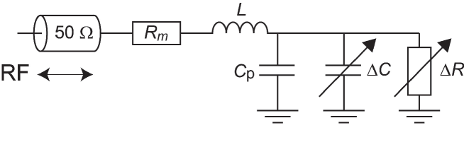
A diagram of the circuit used in this work is shown in Fig. S1. The circuit consists of a capacitance which takes into account the parasitics of the components and wiring, an inductor which consists of the chip inductor placed on the sample holder, and a resistor which takes into account the resistances in the wiring and the inductor - but could also double to allow for a matching resistor. The nanoparticle device, when modeled as a lumped component resistor and capacitor in parallel, as described in Section II below, allows the treatment of the entire system as a simple tank circuit. The impedance of the resonant circuit can then be described as:
| (1) |
Expanding out the terms and arranging into real and imaginary components, we arrive at the impedance of the circuit as a function of the ‘components’ of the device, and .
| (2) |
where . From here, it is possible to understand how a shift in the resistance or capacitance of the device will change the response seen on the circuit. We can simplify this equation by looking at how it behaves near resonance, since this is the nominal operation range - as carried out in the resonant circuit model of Ref. Roschier . Making the (generally good) approximation that and substituting :
| (3) |
where the imaginary component vanishes to zero exactly on resonance. Note that in our work is typically very large, which differs from the work by, e.g., Schoelkopf et al Schoelkopf where the resonant circuit is used to down-convert the resistance of a single-electron transistor (typically of order 10 k) to 50 . From here on, unless explicitly stated, the frequency is assumed to be on resonance. If we define and as the real and imaginary components of the impedance of the circuit, and as the impedance of the wave guide connected to the tank circuit, then the reflection coefficient is given by:
| (4) |
This, along with the calculated impedance from above, can be put together to show how the measured response of the tank circuit will vary as a function of effective dissipative and reactive components of the device, which can be in turn matched to the physics of the device itself using appropriate models.
The amplitude and phase of the reflected signal are given by:
| (5) | ||||
| (6) |
The phase response is a clear indicator of under [] or over [] coupling. In the latter case, the phase change through resonance will be and the former will result in a phase shift of . It is now possible to see how the magnitude and phase of the reflection coefficient vary with relevant factors. For the capacitance shift in phase of the reflection coefficient:
| (7) |
where and is the loaded quality factor of the resonator. In the limit where and this reduces to Eq. 3 in the main text. For the change in reflection magnitude due to a device resistance shift (still assuming ) :
| (8) |
And finally, the change in magnitude due to a capacitance shift:
| (9) |
From this, it can be seen that for a fixed device capacitance, the magnitude shift becomes far more sensitive to resistive changes for a device with smaller resistance. It should also be said that the change of reflection coefficient angle is negligible for changes of device resistance in the case where is large.
II Effective admittance: rate equations
To calculate the effective admittance of the nanoparticle device we start by assuming that we are in the incoherent regime such that the tunnel coupling is sufficiently small: . The tunnel rates for a single electron to tunnel off and on a level at energy relative to the Fermi energy of the tunnel electrode are given by MacLean ; Petersson2 :
| (10) | ||||
| (11) |
where indicates spin degeneracy and is a Fermi function. To simplify the analysis we will use here which does not affect the results - apart from a temperature-dependent shift of the resonance center Bonet which is not important for the analysis below. In the presence of an rf drive, the position of the level relative to the Fermi energy of the tunnel electrode is given by:
| (12) |
where we make use of the lever arm where and are the geometric capacitances between the nanoparticle and the gate electrode and the nanoparticle and the rf electrode, respectively. Typically for our devices and as a result . The probabilities for the level to be either empty () or occupied () by a single charge are:
| (13) | ||||
| (14) |
Since we arrive at the master rate equation:
| (15) |
where we use a small excitation approximation, i.e. . Notice that the gate voltage term cannot be assumed small in comparison with thermal energies. Using for brevity, the solution to this differential equation is a hypergeometric function Arfken :
| (16) |
This can be expressed as a sum:
| (17) |
This is the full response of a single electron revoir with a single lead and single gate to a small oscillation applied to the source. The terms in this sum die off rapidly with increasing n, so by taking the first term (), we can extract much of the physics of the system without too much complexity.
| (18) |
The expected charge drawn from a voltage source connected to the RF electrode at time t is given by . The expected current flowing from the voltage source is then:
| (19) |
The effective impedance is thus:
| (20) |
Equating this with we find that:
| (21) | ||||
| (22) |
Identifying as we arrive at Eq. 1 and 2 in the main text.
III Data analysis and control devices
Using Eq. 7 and Eq. 22 (or Eq. 2 and Eq. 3 in the main text) we are able to fit the measured data to theory, provided and are known. We obtain both from the measured amplitude and phase response over a large frequency range which shows a resonance at MHz. Knowing the value of the chip inductor nH this yields pF. The quality factor is measured by fitting the phase response to: where is the angle at the resonance frequency . This yielded a best fit to the data of . This is somewhat larger than expected for a loaded circuit which we tentatively attribute to an impedance mismatch at the cryogenic amplifier connected to the circuit. For the data fits in the main text we used and the experimentally determined pF and . A constant background slope, seen in all data including control samples, see e.g. Fig. S2b below, has been subtracted.
The full-width-half-maximum (FWHM) of the resonances as a function of gate voltage () described by Eq. 22 provides a relation between temperature and lever arm:
| (23) |
The gate dependency is the differential of the fermi function, as expected. Using Eq. 7 and 22, the maximum phase signal is given by:
| (24) |
From these relations we can determine the temperature and lever arm as:
| (25) |
We are thus able to determine the temperature from measurements of the peak width and height directly which does not require a separate measurement of the lever arm. The signal strength is maximized by improving the lever arm and quality factor. As described in the main text, the devices can be used as a primary thermometer, the limits of which are set by the tunnel coupling and the 0D level spacing and charging energies of the nanoparticles.
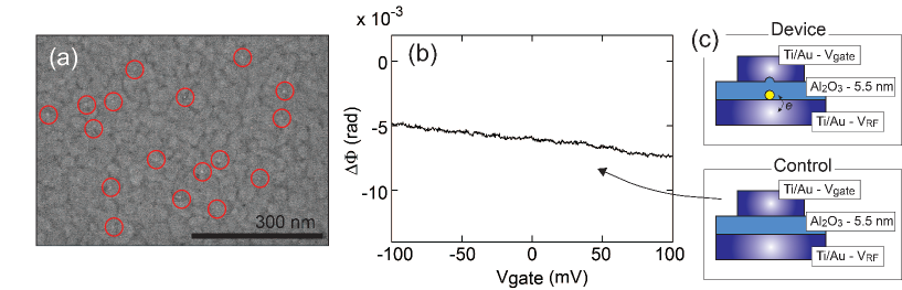
To ensure that we measured the nanoparticles and not some other effect, e.g. charge traps in the oxides, control samples were prepared. When nanoparticles are deposited, a rough indication of the average density is obtained from scanning electron micrographs, see Fig. S2a. For the control devices, exactly the same fabrication procedure as outlined in the Methods section in the main text was carried out, with the exception that no nanoparticles were deposited onto the substrates. All other variables were kept the same, and the various control devices measured. An example is shown in Fig. S2b, for which indeed no signal is observed apart from a slowly decreasing background seen in all devices - leading to the conclusion that the nanoparticles are indeed responsible for resonances in the data. Samples with Au nanoparticles but with considerable thicker gate oxides (> 10 nm Al2O3) also did not show a response at 400 mK (not shown) as expected since for these devices the lever arm will be much smaller and thus the measured signal strength, as expressed by Eq. 24.
References
- (1) Roschier, L. et al. Noise performance of the radio-frequency single-electron transistor, Journal of Applied Physics 95, 1274 (2004).
- (2) Schoelkopf, R.J., Wahlgren, P., Kozhevnikov, A.A., Delsing, P. and Prober, D.E. The radio-frequency single-electron transistor (RF-SET): A fast and ultrasensitive electrometer. Science 280, 1238 (1998).
- (3) MacLean, K. Energy-dependent tunneling in a quantum dot. Phys. Rev. Lett. 98, 036802 (2007).
- (4) Petersson, K.D., PhD thesis: High frequency manipulation and measurement of charge and spin states in GaAs quantum dot devices, Cambridge (UK), 2009.
- (5) Bonet, E. Deshmukh, M.M. and Ralph, D.C. Solving rate equations for electron tunneling via discrete quantum states, Phys. Rev. B 65, 045317 (2002).
- (6) Arfken, G.B and Weber, H.J. Mathematical methods for physicists, 6ed edition, Elsevier Academic Press (2005).