Suppression of Spin Pumping Between Ni80Fe20 and Cu by a Graphene Interlayer
Abstract
We compare ferromagnetic resonance measurements of Permalloy Ni80Fe20 (Py) films sputtered onto Cu(111) films with and without a graphene (Gr) interlayer grown by chemical vapor deposition before Py deposition. A two-angle sputtering method ensured that neither Gr nor Py was degraded by the sample preparation process. We find the expected damping enhancement from spin pumping for the Py/Cu case and no detectable enhancement for the Py/Gr/Cu case. Since damping is sensitive to effects other than spin pumping, we used magnetometry to verify that differences in Py magnetostatic properties are not responsible for the difference in damping. We attribute the suppression of spin pumping in Py/Gr/Cu to the large contact resistance of the Gr/Cu interface.
I Introduction
The complex interactions between magnetization dynamics in a ferromagnet and the flow of charge and spin currents is a topic that combines rich physics and relevance to technological applications. These interactions are often divided into two types that are reciprocal manifestations of the same microscopic process (Brataas and Hals, 2014). Spin transfer refers to the torque exerted on the magnetization by a flow of spins (with or without an associated flow of charge). Spin pumping refers to the flow of spins generated by a precessing magnetization. The first effect enables control of magnetization through an applied current (Ralph and Stiles, 2008), rather than an applied magnetic field, and is crucial to realizing a scalable magnetic random access memory (Ando et al., 2014). The second effect is most often encountered as an enhanced damping of magnetization dynamics when a thin ferromagnetic (FM) film is in contact with a nonmagnetic (NM) material that absorbs the spin current (Tserkovnyak et al., 2002, 2002). This loss of angular momentum adds to the intrinsic dissipation of the FM material, causing an enhancement of the Gilbert damping parameter . The effect on damping can be quite large for ultrathin FM films and has been observed for many FM/NM combinations (Tserkovnyak et al., 2002; Xia et al., 2002; Bauer et al., 2003; Gerrits et al., 2006; Shaw et al., 2012; Mizukami et al., 2001, 2001).
Brataas et al. (Brataas and Hals, 2014) have reviewed the phenomenology and the quantitative theory of spin transfer and spin pumping. When considering the effect of spin pumping on FM damping, it is useful to identify two limiting cases. If the FM is in contact with a material that strongly scatters or absorbs the pumped spin current, is increased substantially. In contrast, if the NM does not act as a spin sink, then pumped spins will accumulate in the NM and drive a diffusive spin current back toward the FM that cancels the spin pumping current in steady state. In this “spin battery” limit, there is no effect on . For a general case, the change in damping for a FM film of thickness is determined by an effective spin conductance per unit area, (units of ), according to
| (1) |
where is the gyromagnetic ratio, is the electron charge, is the reduced Planck constant, and is the saturation magnetization of the FM. The conductance includes contributions from the FM/NM interface and from spin diffusion in the NM material (see Appendix A).
Graphene (Gr) is expected to be a useful material for spintronics because its high carrier mobility and low spin scattering should allow propagation of spin currents over long distances at room temperature. Spin coherence lengths of about have been demonstrated by injecting spin-polarized charge current from FM contacts into a Gr channel (Han et al., 2012). The main challenge facing these devices is the limited efficiency for injecting spin-polarized carriers from the metallic FM into a channel having much lower electrical conductivity. Even with tunnel barriers between the FM and the Gr designed to minimize this effect, the efficiency is only about 30% (Han et al., 2012). Since spin pumping involves only spins and not charges flowing between the FM and NM materials, it provides a way to inject spin current from FM metals into Gr that is not limited by the mismatch in electrical conductivity.
This paper compares ferromagnetic resonance (FMR) measurements of Permalloy Ni80Fe20 (Py) films with nominal thicknesses between 8 nm and 45 nm sputtered onto Cu(111) films with and without a Gr interlayer grown by chemical vapor deposition (CVD) before Py deposition. The Py films were deposited using a two-step process (see section III.1) that avoids damage to the Gr and yields high quality Py. The FMR results show the expected damping enhancement for the Py/Cu case but no enhancement for the Py/Gr/Cu case. This unexpectedly strong effect on spin tranport by a monolayer of material with weak intrinsic spin scattering requires careful validation. Since FM damping is sensitive to effects other than spin pumping, much of the paper is concerned with ensuring that neither Gr nor Py is significantly degraded by the sample preparation process. In particular, we use a novel two-angle sputtering geometry, we verify the Gr quality using Raman spectroscopy, we use magnetometry to measure the moment and coercivity of each sample, and we examine the Py morphology using transmission electron microscopy.
Previous studies have shown evidence for spin pumping from Py into Gr (Tang et al., 2013; Singh et al., 2015), but the use of only a single thickness of Py and the lack of magnetometry or other characterization of the Py itself limits the conclusions that can be drawn from the observed effects. We discuss these limitations in detail, drawing on our results and on other recently published work (Berger et al., 2014). Finally, we attribute the suppression of spin pumping in Py/Gr/Cu to the large contact resistance of the Gr/Cu interface (Robinson et al., 2011).
II FMR Measurement of Spin Pumping
For FMR measurements, samples were placed on a coplanar waveguide with a center conductor width of , and the scattering parameter was measured using a vector network analyzer. The static magnetic field was applied perpendicular to the sample plane and was large enough to saturate the magnetization, suppressing the 2-magnon scattering contribution to the FMR linewidth (McMichael and Krivosik, 2004). For each excitation frequency , fitting the real and imaginary parts of yields the resonance field and the field-swept linewidth . Details of the measurement and data analysis techniques are described in (Nembach et al., 2011).
The FMR resonance field and linewidth as a function of excitation frequency are given by
| (2) |
| (3) |
where is the magnetic constant, is the effective magnetization including a perpendicular anisotropy field , and is the broadening due to inhomogeneity in the local resonance field across the sample (Nembach et al., 2011). A linear fit to Eq. 2 gives values for and , and a linear fit to Eq. 3 gives values for and (Nembach et al., 2011). Results for all four fitted parameters are given in Appendix B.
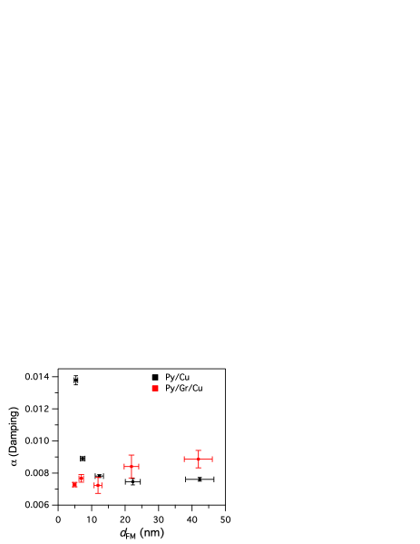
Figure 1 shows as a function of for two sets of Py samples. The Py/Cu samples clearly show an increase in as decreases, as seen previously (Gerrits et al., 2006) and as expected from Eq. 1, while the Py/Gr/Cu samples show no significant change in . As shown in the next section, the Py in the two sets of samples has very similar magnetic and morphological properties, so this result is strong evidence for suppression of spin pumping between Py and Cu due to the Gr interlayer.
III Sample Preparation and Characterization
III.1 Motivation for Two-angle Sputtering
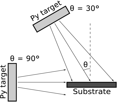
Damage to Gr during magnetron sputtering of Ti and Al has been studied using Gr flakes exfoliated onto Si substrates (Chen et al., 2013). This work considered several types of bombardment present in sputtering (electrons, photons, depositing atoms, and inert gas atoms) and concluded that damage is primarily due to inert gas atoms, which can be reflected from the target as neutral atoms with sufficient energy to displace C atoms from Gr. Detailed simulations (Yamamura and Ishida, 1995) of sputtering a Cu target in Ar gas show, for a typical discharge voltage of 400 V, that Cu atoms leave the target with an average energy of about 10 eV, while Ar neutrals are reflected with an average energy of about 45 eV. For comparison, the displacement threshold for Ar striking Gr at normal incidence is 33 eV (Lehtinen et al., 2010, 2011). Increasing the gas pressure or target-to-substrate distance reduces the flux of both Ar neutrals and depositing atoms, but since the more energetic Ar atoms have a longer mean free path than the depositing atoms (Yamamura and Ishida, 1995), the deposition rate is strongly suppressed before the Gr is protected from Ar impacts. Since the displacement threshold increases away from normal incidence (Lehtinen et al., 2010, 2011), damage can be avoided by orienting the substrate perpendicular to the target, as seen in Fig. 2 with . The tradeoff between deposition rate and Gr damage for orientations near perpendicular was quantified for Ti and Al in (Chen et al., 2013).
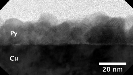
For many magnetic materials, including Py, bombardment of the substrate is important in promoting growth of thin films that are homogeneous and have properties such as and that are close to bulk values. Thus a substrate orientation perpendicular to the target is undesirable in terms of film quality as well as deposition rate. For this reason, we chose to deposit Py at two separate orientations, as shown in Fig. 2. The first deposition, 5 nm at , covers the Gr with a Py film of low quality but does not damage the Gr, and this Py layer protects the Gr from damage during the second deposition, at , that yields high quality Py. The two depositions were done without breaking vacuum by use of an angled sample holder (see Methods section). Importantly, transmission electron microscopy (see Section III.3 and Fig. 5) shows the final Py film to be a single, homogeneous layer rather than two distinct layers. We attribute the lack of a morphological boundary between the two layers to bombardment during the second deposition. The sum of the first and second deposition thicknesses is the nominal Py thickness, .
III.2 Gr Properties
We used Raman spectroscopy to measure Gr damage as follows. The Raman spectrum of pristine Gr has two characteristic peaks, named G and 2D, and defects allow an additional scattering mechanism that adds a feature named the D peak (Ferrari and Basko, 2013). The ratio of the peak intensities for the D and G features, , can be used to estimate the number of point defects per unit area (Cançado et al., 2011).
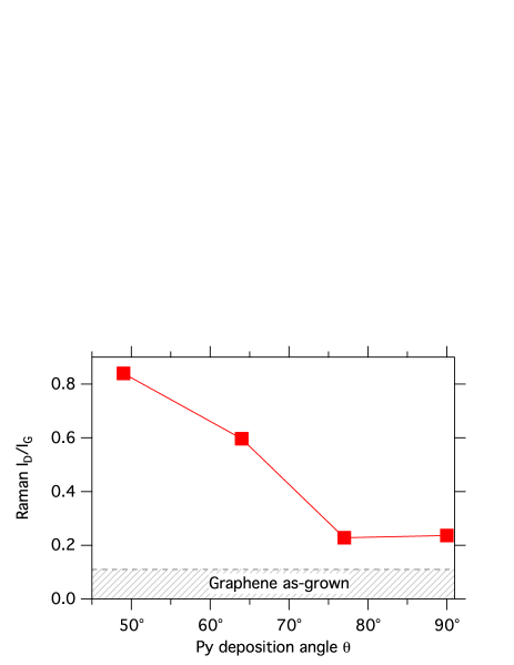
For our as-grown Gr on Cu, we found a baseline value of , which implies one defect every . We deposited 5 nm to 35 nm of Py at on several samples and found no change in , demonstrating that sputtering in this geometry does not damage Gr. The fact that Gr Raman peaks could be measured through these films indicates the Py deposited at was highly transparent, consistent with the fact that these samples still showed some Cu color after deposition. In contrast, Py deposited at did not show any Gr Raman peaks for thickness and had a color similar to that of high quality Ni films. A short deposition at , lasting and giving , allowed us to measure Gr Raman peaks with , corresponding to one defect every . This confirms that Gr is readily damaged by sputtering in this geometry, with a damage rate of roughly . In fact, this rate is close to the flux of Ar neutrals expected from the simulations in (Yamamura and Ishida, 1995) (see Appendix C).
We estimated the potential damage to Gr covered by Py using the Stopping and Range of Ions in Matter (SRIM) Monte Carlo simulation (Ziegler et al., 2010). Since the substrate in our case is located 23 cm from the target, only Ar neutrals reflected nearly perpendicular to the target will reach the substrate, with a maximum energy of 70 eV for a 430 V discharge (Yamamura and Ishida, 1995). For Ar ions at 70 eV and normal incidence, SRIM predicts no transmission for 5 nm of Py with its nominal density of . Adjusting parameters to reflect the fact that Py deposited at is different from nominal, e.g., using a thickness of 2 nm and nominal density, or a thickness of 5 nm and a density of , yielded a transmission probability of less than 1 in . Combining this with the Ar neutral flux estimated in Appendix C shows that damage due to Ar penetration through the Py film is expected to be negligible.
III.3 Py properties
In addition to FMR measurements, we used vibrating sample magnetometry (VSM) to measure Py magnetostatic properties of the same samples presented in Fig. 1. We also used transmission electron microscopy (TEM) to characterize Py morphology for separate, similarly prepared samples.
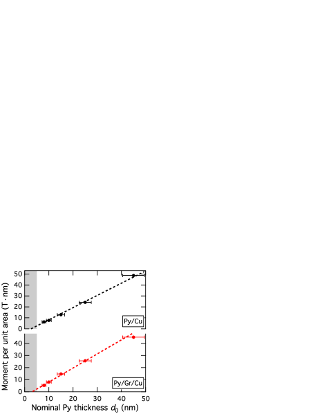
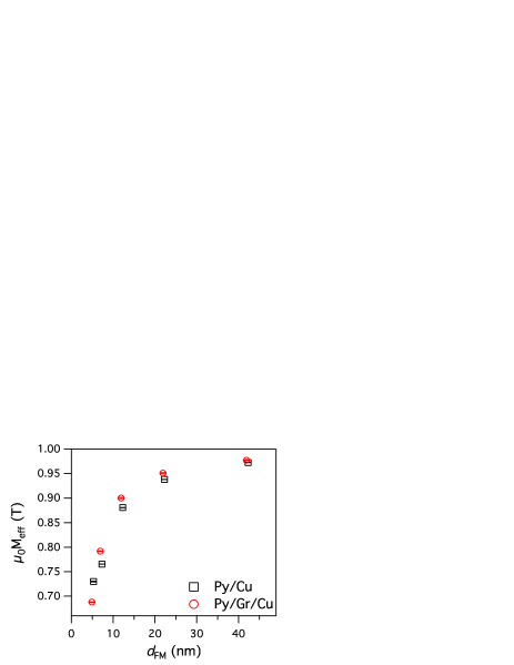
For a homogeneous FM film with magnetization and thickness , the moment per unit area is . The total magnetic moment measured by VSM, divided by the area of each sample, is plotted vs. nominal Py thickness in Fig. 3. From the slopes of the linear fits in Fig 3, we find for both Py/Cu and Py/Gr/Cu samples. The nonzero intercepts of the fits imply the actual thickness of the films is less than the nominal thickness. This is not surprising, since the 5 nm of Py deposited at is porous (see Section III.2) and some of the Py deposited at will fill the pores instead of adding to the overall film thickness. For the rest of this paper, we use the actual FM thickness obtained by subtracting the intercept values from .
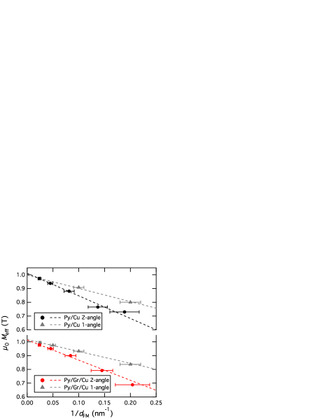
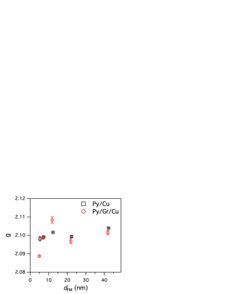
Given the actual FM thickness values, we can use measured by FMR to determine the perpendicular anisotropy of the Py as follows. Figure 4 shows plots of vs. for the two-angle Py/Cu and Py/Gr/Cu samples, and for several samples deposited only at . The linear dependence for all samples is consistent with a constant interfacial anisotropy energy , for which is given by
Thus the intercept of each linear fit in Fig. 4 gives and the slope gives . We find for both Py/Cu and Py/Gr/Cu samples, consistent with the value obtained from VSM data. The values of , given in Table 1, are quite similar for a given deposition method, but are noticeably larger for two-angle films than for single-angle films. Furthermore, our values are larger than the value of reported for Py/Cu (Rantschler et al., 2005) and Py/air (Bailey and Vittoria, 1973) interfaces. These differences are likely due to variations is how Py nucleates and grows on different substrates, for example polycrystalline Cu compared to our Cu(111), in addition to the different deposition geometries.
| Py/Cu, two-angle | |
|---|---|
| Py/Gr/Cu, two-angle | |
| Py/Cu, | |
| Py/Gr/Cu, |
The coercive field measured by VSM is 0.5 mT for Py/Cu and 0.25 mT for Py/Gr/Cu. Although both values are somewhat larger than the typically found for high-quality Py, similar values have been reported for Py deposited on Cu(111) single crystals (Rook et al., 1991). Finally, a 40 nm Py/Cu film deposited at a single angle of showed the same value of () as the two-angle Py/Cu film with 5 nm at and 40 nm at , indicating that the intrinsic damping of the Permalloy is not affected by two-angle deposition.
Overall, these results show that whatever effects Gr may have on the film growth process, for our two-angle method it has little or no effect on the Py magnetic properties.
We prepared samples for cross-sectional TEM imaging using a standard lift-out technique in a focused ion beam microscope (Giannuzzi et al., 1997). Following a thinning step using 5 kV Ga+ ions, we performed a final cleaning and thinning using 900 eV Ar+ ions.
An image of a two-angle Py film deposited on Gr/Cu, 10 nm at and 10 nm at , is shown in Fig. 5. While the film is quite rough, it is continuous and, importantly, shows neither internal voids nor an apparent boundary between the two Py layers. This suggests that any holes in the first layer are filled in during the second deposition. The Py grains are fairly round and selected area diffraction patterns (not shown) indicate a modest (111) texture.
IV Discussion
Since our co-deposited Py/Cu and Py/Gr/Cu films have the same magnetization, similar perpendicular anisotropies, and nearly the same damping for films 15 nm and thicker, the dramatic difference in damping for thinner films (see Fig. 1) must be attributed to the Gr interlayer. We do not expect other effects such as surface oxidation and surface roughness to be substantially different between the two types of samples. This leads to the surprising conclusion that a single layer of C atoms can block the transfer of spins between two metals. Before offering an explanation for this effect, we first compare our results with other FMR measurements of Py films deposited on Gr.
In (Patra et al., 2012) and (Singh et al., 2015), Gr grown by CVD on Cu foils was transferred to insulating or semiconducting substrates and Py was deposited by thermal evaporation to give Py/substrate and Py/Gr/substrate samples. Only a single Py thickness, 14 nm, was used for all samples in these two studies. In (Patra et al., 2012), for samples where the Py covered the entire Gr area, the Py damping was 1.9 times larger when Gr was present. This was interpreted as evidence for strong spin scattering in Gr itself, which would be contrary to all expectations. However, was also different for these samples (30% lower with Gr present) which suggests the difference in damping could be due to differences in the Py itself rather than the presence of Gr. In (Singh et al., 2015), the same group made Py/Gr samples where the Gr extended past two edges of the Py film. Damping for these sample was 1.1 times larger than for similar samples where the Py covered the entire Gr area. This small change in damping cannot be reliably attributed to spin pumping without further measurements to rule out changes in the Py. Unfortunately, no independent measurements of or were reported in (Patra et al., 2012) or (Singh et al., 2015). Further evidence of the need for caution comes from a study of 14 nm thick Co films deposited by evaporation onto Gr/SiO2 and SiO2 substrates (Berger et al., 2014). Careful characterization by FMR, magnetometry, magnetic force microscopy, and Kerr microscopy revealed such clear magnetic differences between the samples that the authors, commendably, declined to draw any conclusions about spin pumping into Gr.
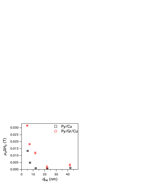
In (Tang et al., 2013), Py and Pd were evaporated onto a Gr/SiO2 substrate and patterned into stripes separated by about of unpatterned Gr. When the Py was driven to precess by an magnetic field, a voltage was detected in the Pd stripe that behaved as expected if a spin current was pumped from the Py into the Gr channel and then generated an inverse spin Hall voltage after diffusing to the Pd. FMR measurements at this same frequency showed the linewidth for Py/Gr/SiO2 was 0.5 mT larger than for Py/SiO2, for 25 nm thick Py. This difference was attributed to spin pumping from Py to Gr, but since was not measured the difference could equally be due to differences in the Py itself. The fact that for our 25 nm Py films differed by 0.9 mT, while differed by only 1%, shows that FMR linewidth at a single frequency does not yield a reliable estimate for damping or spin pumping.
The limitations of these previous experiments can be avoided by varying both FMR frequency and FM thickness over a wide range. The frequency range reveals what fraction of FMR linewidth is due to damping () as opposed to inhomogeneity (). The plot of vs. allows a clear separation of the intrinsic and spin pumping contributions to at each thickness.
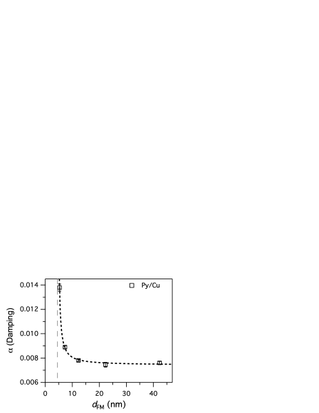
For our Py/Cu samples, the spin pumping expression in Eq. 1 can be fit to the data shown in Fig. 1 and reproduced in Fig. 6. For this fit we used the value of calculated from the data in Fig. 4. We also added an adjustable thickness , representing a Py “dead layer” that does not contribute to spin pumping. Finally, we added an adjustable intrinsic damping to account for non-zero damping at large thickness. The fit then yields , , and , and is shown by the dashed curve in Fig. 6. The uncertainty in is largely due to uncertainty in the thickness of the thinnest film.
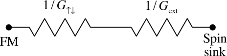
As described in Appendix A, we use a model for that combines an interfacial spin mixing conductance and an external conductance as resistors in series, i.e.,
| (4) |
The interfacial contribution is of order (see Appendix A), so in our case is dominated by and insensitive to the value of . We can therefore neglect and, using the expression for given in Appendix A and a bulk conductivity for Cu of , we infer a spin diffusion length in Cu of . This value is roughly consistent with the various room temperature values compiled in (Bass and Pratt, 2007).
While we are unable to find prior measurements of spin pumping dead layers at Py/Cu interfaces, measurements on other FM/NM systems show much thinner dead layers, (Boone et al., 2013). This could be due to differences in the Py/Gr interface due to our unusual deposition conditions. Additionally, our 1-D spin pumping model does not account for lateral sample inhomogeneity, such as that from roughness observed in Fig. 5, but the effect of in-plane spin currents on our parameters is unknown.
A likely explanation for the dramatic suppression of spin pumping by a single Gr layer is the electrical contact resistance between Gr and Cu. Measurements for several metals deposited on Gr gave a value of for Cu and values of for Ni, Ti, Pd, and Pt (Robinson et al., 2011). Adding this term to Eq. 4, we expect for Py/Gr/Cu, which is nearly 5 orders of magnitude smaller than for Py/Cu. Thus the Gr/Cu interface presents a large barrier to spin flow, reducing the net flow of spin current away from the Py to the point where even our thinnest films show no enhanced damping.
Even the lowest metal-Gr contact resistances are much larger than , which raises the question of whether spin pumping into Gr is possible under any conditions. Although the values of and inferred in (Tang et al., 2013) depend entirely on a questionable value for , the voltage detected at the Pd in those experiments is strong evidence that spins did flow from the Py to the Pd. Given this evidence, we believe it is likely that in our Py/Gr/Cu samples there is significant spin pumping into the Gr, but also a large spin accumulation because of the barrier at the Gr/Cu interface and therefore a large diffusion of spins back into the Py. A quantitative understanding of this situation, in which the same monolayer of C atoms participates in both the Py/Gr and the Gr/Cu interfaces, is a rich topic for further investigation.
V Conclusion
In summary, we prepared Py/Cu and Py/Gr/Cu samples with varying Py thickness , using a two-angle sputtering method and carefully verifying that neither Gr nor Py were degraded. We used FMR to measure damping for both series of samples. The Py/Cu samples showed an increase in with decreasing , as expected from spin pumping. Fitting the standard model of spin pumping showed was dominated by of the Cu rather than the interfacial conductance , which precludes determining a value for the latter. The Py/Gr/Cu samples, despite having the same Py properties, showed no change in damping with thickness. This implies a strong suppression of spin flow away from the Py, which we attribute to the large contact resistance at the Gr/Cu interface.
Our results are consistent with the evidence for spin pumping from Py into Gr reported in (Tang et al., 2013), where an inverse spin Hall voltage was detected at a separate Pd electrode. However, we emphasize that quantitative analysis of spin pumping data requires independent characterization of magnetic properties and a consideration of the effect of all relevant conductances, not only . Our results are not consistent with the interpretation offered in (Patra et al., 2012) that Gr itself is a strong spin absorber. We expect that magnetometry and/or a thickness series would show that differences in Py properties, rather than spin pumping, are responsible for the change in damping in this case.
VI Methods
VI.1 Cu film deposition and Gr CVD
Epitaxial, crystalline Cu(111) thin films on sapphire were made as described in (Miller et al., 2013). In brief, 500 nm of Cu was sputtered onto 50 mm wafers of -Al2O3(0001) held at . During the annealing that preceded Gr growth (see below), secondary grain growth resulted in exclusively Cu(111) grains across. These large grains prevent dewetting of the Cu film during Gr CVD at higher temperatures (Miller et al., 2013). One Cu/Al2O3 wafer was removed after annealing only and used for Py deposition directly on Cu, while a second wafer continued through the Gr growth step.
Gr CVD was performed in a hot-wall quartz tube furnace with a diameter of 76 mm. After evacuating the tube with a dry pump to a pressure of (5 mTorr), the rest of the process was performed at a total pressure of (600 Torr). The wafer was heated in a flow of 7 sccm H2 and 2100 sccm Ar (H2 partial pressure of (2 Torr)), initially ramping to in about 15 min and then moving to at to allow complete Cu grain growth. The temperature was then increased to C and the gas flows were changed to 58 sccm H2 and 3600 sccm Ar (H2 partial pressure of (9.5 Torr)). After 10 min under these conditions, Gr growth was initiated by adding 18 sccm of 0.2% CH4 in Ar (CH4 partial pressure of (6 mTorr)). Growth conditions were maintained for 3 h before rapid cooling by opening the furnace lid. The flow of CH4 was stopped below C and the flow of H2 was stopped below .
The resulting Gr films were characterized by optical microscopy to check for completeness of growth and Raman spectroscopy to confirm their quality. For shorter growth times, for which Gr coverage was incomplete, we found this growth recipe consistently gave compact hexagonal Gr growth domains with nucleation sites separated by .
Both wafers were cut into 6 mm 8 mm chips using a diamond scribe.
VI.2 Py sputter deposition
For each thickness, Py was deposited simultaneously onto bare Cu and Gr/Cu samples. To remove Cu oxide and adventitious contamination, samples were soaked in glacial acetic acid for 1 min and rinsed in deionized water just prior to being placed in the load lock of a deposition chamber with a base pressure (). The samples were heated to to remove residual water and then cooled in vacuum to before deposition. Depositions at both and were performed with the source running at 200 W and , in 1.1 mTorr of Ar gas, and with a target-to-sample distance of 23 cm. The deposition rates, measured using atomic force microscopy for thick films, were for and for .
VI.3 Magnetometry
The VSM measurements were performed at room temperature with the sample mounted in a plastic straw, using a frequency of 40 Hz, and an oscillation amplitude of 2 mm. The magnetic field, applied in the plane of the sample, was swept over a range of 4 T to allow a linear fit to the diamagnetic background, due primarily to the Al2O3 substrate. The moment of the Py layer was taken as the intercept value of a linear fit from 1 T to 4 T.
VI.4 Raman spectroscopy
We performed Raman spectroscopy in a home-built system using a 532 nm diode laser with a power of and a spot size . Peak fitting was done after subtracting a smooth fit to the surrounding background from Cu fluorescence.
Acknowledgments
The authors thank Justin Shaw for valuable comments on interfacial anisotropy in Py, Bill Rippard and Justin Shaw for help in maintaining the sputter deposition chamber, and Ben Derby for help in sample preparation. Optical microscopy and TEM were done in NIST’s Precision Imaging Facility.
Author contributions
MWK, TJS, and WJG designed the experiments. WJG made the Gr/Cu substrates, deposited the Py films, and performed VSM and Raman measurements. HTN performed FMR measurements and TJS peformed FMR data analysis. ACD performed TEM sample preparation and imaging. MWK developed the two-angle sputtering method. MWK and WJG wrote the manuscript. All authors contributed to interpretation of the data and commented on the manuscript.
APPENDIX A: Model for Spin Pumping in Multi-Layer Structures
Following (Boone et al., 2013), we model the spin transport of a FM layer in contact with one or more NM layers as an electrical circuit of resistors in series. Fig. 7 shows the simplest case of one interfacial resistance, , and one external resistance, , The effective conductance for spin current flowing from the FM to the spin sink is simply
Since these conductances describe spin transport perpendicular to the FM/NM interface, they are defined per unit area of the interface and have units of . In the full theory of spin pumping (Brataas and Hals, 2014), is a complex quantity whose real part affects damping and whose imaginary part affects the FM precession frequency. For conventional FM metals such as Ni, Fe, and Co, the effect on frequency is negligible (Zwierzycki et al., 2005) and is commonly used to refer only to the real part.
The interfacial conductance , often called the “spin-mixing” conductance, determines how readily spins can move across the FM/NM interface. This process is governed by the exchange interaction, which operates over a length scale of a few nanometers. For metallic interfaces, the theoretical upper bound on (Bauer et al., 2003) is the Sharvin conductance (Sharvin, 1965) (for a single spin direction and per unit area), corresponding to perfect transmission for every conductance channel at the interface,
where is the Fermi wavevector. Taking Cu as a typical metal, with , we find . Both experimental and theoretical results for Py/Cu interfaces (and several other FM/NM combinations) are consistent with this limit (Tserkovnyak et al., 2002; Xia et al., 2002; Bauer et al., 2003; Gerrits et al., 2006; Shaw et al., 2012), with in the range of .
The external conductance determines how readily spins flow away from the interface once they have entered the NM material. For a single NM layer of thickness , bulk electrical conductivity , and spin diffusion length , is given in (Boone et al., 2013) as
For , which is often the case, the external spin conductance is simply determined by the ratio of conductivity and spin diffusion length, .
In the limit of , when spins diffuse rapidly away from the interface, and a measurement of can be used to directly infer a value of from Eq. 1. This limit applies to NM materials with large and/or small , such as Pt and Pd (Boone et al., 2013). However, other materials such as Ta and Cu (Boone et al., 2013) are in the opposite limit, where and is not sensitive to .
APPENDIX B: Full FMR Results
Table 2 shows all parameters obtained by fitting the FMR data for each sample. These results are plotted in Figs. 8, 9, and 10. Values of come from fits to Equation 2, where .
| (nm) | (T) | (mT) | |||
|---|---|---|---|---|---|
| Cu+Gr | 5+3 | 0.6879 | 2.089 | 31.6 | 0.00730.0001 |
| 5+3 | 0.7918 | 2.098 | 18.2 | 0.00770.0002 | |
| 5+10 | 0.9002 | 2.108 | 11.9 | 0.00720.0005 | |
| 5+20 | 0.9509 | 2.097 | 1.7 | 0.00840.0007 | |
| 5+40 | 0.9772 | 2.102 | 3.2 | 0.00890.0005 | |
| Cu | 5+3 | 0.7298 | 2.098 | 13.4 | 0.01380.0003 |
| 5+5 | 0.7654 | 2.099 | 4.9 | 0.00890.0001 | |
| 5+10 | 0.8807 | 2.102 | 0.9 | 0.00780.0001 | |
| 5+20 | 0.9381 | 2.099 | 0.8 | 0.00750.0002 | |
| 5+40 | 0.9725 | 2.104 | 1.1 | 0.00760.0001 |
APPENDIX C: Graphene Damage Estimates
Expected Damage Rate from Ar Neutrals
The simulation results in (Yamamura and Ishida, 1995) can be applied to our sputtering conditions to estimate the flux of Ar neutrals arriving at the substrate with sufficient energy to damage the Gr. In particular, the results in Fig. 7 of (Yamamura and Ishida, 1995) for 400 eV Ar+ ions hitting a Cu target are a good estimate for our case of 430 eV Ar+ hitting a Ni80Fe20 target. The probability of an Ar neutral reflected normal to the target and with sufficient energy to damage Gr is approximately per unit solid angle for each Ar+ ion that hits the target. Our sputtering source operates at a current of 0.47 A, corresponding to Ar+ ions per second. Our substrate, oriented at and at a distance of 230 mm from the target, subtends a solid angle of . The result in Fig. 21 of (Yamamura and Ishida, 1995) shows that there is negligible scattering of Ar neutrals for our pressure-distance product of . This yields a flux of damaging Ar neutrals at our substrate of about , remarkably close to the value of inferred from the Raman spectrum of the 2 s exposure described in the main text.
Raman Measurement of Gr Damage vs. Angle
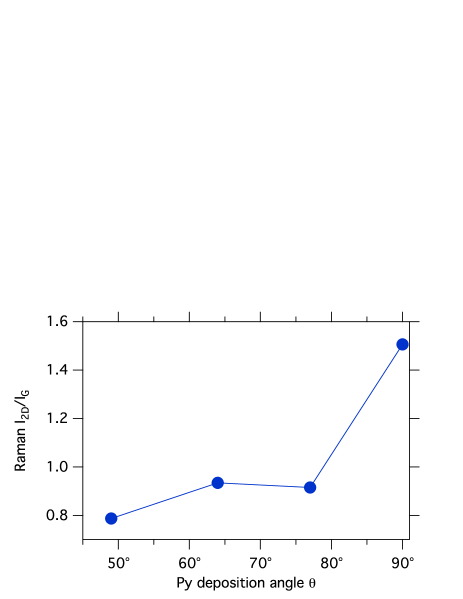
In order to evaluate Gr damage as a function of sputtering angle, we deposited of Py at several angles between and and made Raman measurements. The results for and are shown in Fig. 11.
References
- Brataas and Hals (2014) A. Brataas and K. M. D. Hals, Nature Nano., 9, 86 (2014).
- Ralph and Stiles (2008) D. C. Ralph and M. D. Stiles, J. Magn. Magn. Mater., 320, 1190 (2008).
- Ando et al. (2014) K. Ando, S. Fujita, J. Ito, S. Yuasa, Y. Suzuki, Y. Nakatani, T. Miyazaki, and H. Yoda, J. Appl. Phys., 115, 172607 (2014).
- Tserkovnyak et al. (2002) Y. Tserkovnyak, A. Brataas, and G. E. W. Bauer, Phys. Rev. Lett., 88, 117601 (2002a).
- Tserkovnyak et al. (2002) Y. Tserkovnyak, A. Brataas, and G. E. W. Bauer, Phys. Rev. B, 66, 224403 (2002b).
- Xia et al. (2002) K. Xia, P. J. Kelly, G. E. W. Bauer, A. Brataas, and I. Turek, Phys. Rev. B, 65, 220401 (2002).
- Bauer et al. (2003) G. E. W. Bauer, Y. Tserkovnyak, D. Huertas-Hernando, and A. Brataas, Phys. Rev. B, 67, 094421 (2003).
- Gerrits et al. (2006) T. Gerrits, M. L. Schneider, and T. J. Silva, J. Appl. Phys., 99, 023901 (2006).
- Shaw et al. (2012) J. M. Shaw, H. T. Nembach, and T. J. Silva, Phys. Rev. B, 85, 054412 (2012).
- Mizukami et al. (2001) S. Mizukami, Y. Ando, and T. Miyazaki, J. Magn. Magn. Mater., 226–230, 1640 (2001a).
- Mizukami et al. (2001) S. Mizukami, Y. Ando, and T. Miyazaki, Jap. J. Appl. Phys., 40, 580 (2001b).
- Han et al. (2012) W. Han, K. McCreary, K. Pi, W. Wang, Y. Li, H. Wen, J. Chen, and R. Kawakami, J. Magn. Magn. Mater., 324, 369 (2012).
- Tang et al. (2013) Z. Tang, E. Shikoh, H. Ago, K. Kawahara, Y. Ando, T. Shinjo, and M. Shiraishi, Phys. Rev. B, 87, 140401 (2013).
- Singh et al. (2015) S. Singh, A. Ahmadi, C. T. Cherian, E. R. Mucciolo, E. del Barco, and B. Özyilmaz, Appl. Phys. Lett., 106, 032411 (2015).
- Berger et al. (2014) A. J. Berger, W. Amamou, S. P. White, R. Adur, Y. Pu, R. K. Kawakami, and P. C. Hammel, J. Appl. Phys., 115, 17C510 (2014).
- Robinson et al. (2011) J. A. Robinson, M. LaBella, M. Zhu, M. Hollander, R. Kasarda, Z. Hughes, K. Trumbull, R. Cavalero, and D. Snyder, Appl. Phys. Lett., 98, 053103 (2011).
- McMichael and Krivosik (2004) R. McMichael and P. Krivosik, IEEE Trans. Magn., 40, 2 (2004).
- Nembach et al. (2011) H. T. Nembach, T. J. Silva, J. M. Shaw, M. L. Schneider, M. J. Carey, S. Maat, and J. R. Childress, Phys. Rev. B, 84, 054424 (2011).
- Chen et al. (2013) C.-T. Chen, E. A. Casu, M. Gajek, and S. Raoux, Appl. Phys. Lett., 103, 033109 (2013).
- Yamamura and Ishida (1995) Y. Yamamura and M. Ishida, J. Vac. Sci. Technol. A, 13, 101 (1995).
- Lehtinen et al. (2010) O. Lehtinen, J. Kotakoski, A. V. Krasheninnikov, A. Tolvanen, K. Nordlund, and J. Keinonen, Phys. Rev. B, 81, 153401 (2010).
- Lehtinen et al. (2011) O. Lehtinen, J. Kotakoski, A. V. Krasheninnikov, and J. Keinonen, Nanotechnology, 22, 175306 (2011).
- Ferrari and Basko (2013) A. C. Ferrari and D. M. Basko, Nature Nano., 8, 235 (2013).
- Cançado et al. (2011) L. G. Cançado, A. Jorio, E. H. M. Ferreira, F. Stavale, C. A. Achete, R. B. Capaz, M. V. O. Moutinho, A. Lombardo, T. S. Kulmala, and A. C. Ferrari, Nano Lett., 11, 3190 (2011).
- Ziegler et al. (2010) J. F. Ziegler, M. Ziegler, and J. Biersack, Nuclear Instrum. Meth. Phys. B, 268, 1818 (2010).
- Rantschler et al. (2005) J. O. Rantschler, P. J. Chen, A. S. Arrott, R. D. McMichael, W. F. Egelhoff, and B. B. Maranville, J. Appl. Phys., 97, 10J113 (2005).
- Bailey and Vittoria (1973) G. C. Bailey and C. Vittoria, Phys. Rev. B, 8, 3247 (1973).
- Rook et al. (1991) K. Rook, A. M. Zeltser, J. O. Artman, D. E. Laughlin, M. H. Kryder, and R. M. Chrenko, J. Appl. Phys., 69, 5670 (1991).
- Giannuzzi et al. (1997) L. A. Giannuzzi, J. L. Drown, S. R. Brown, R. B. Irwin, and F. A. Stevie, MRS Proceedings, 480, 19 (1997).
- Patra et al. (2012) A. K. Patra, S. Singh, B. Barin, Y. Lee, J.-H. Ahn, E. del Barco, E. R. Mucciolo, and B. Özyilmaz, Appl. Phys. Lett., 101, 162407 (2012).
- Bass and Pratt (2007) J. Bass and W. P. Pratt, J. Phys. Condens. Matter, 19, 183201 (2007).
- Boone et al. (2013) C. T. Boone, H. T. Nembach, J. M. Shaw, and T. J. Silva, J. Appl. Phys., 113, 153906 (2013).
- Miller et al. (2013) D. L. Miller, M. W. Keller, J. M. Shaw, K. P. Rice, R. R. Keller, and K. M. Diederichsen, AIP Advances, 3, 082105 (2013).
- Zwierzycki et al. (2005) M. Zwierzycki, Y. Tserkovnyak, P. J. Kelly, A. Brataas, and G. E. W. Bauer, Phys. Rev. B, 71, 064420 (2005).
- Sharvin (1965) Y. V. Sharvin, Sov. Phys. JETP, 21, 655 (1965).