Tuning equilibration of quantum Hall edge states in graphene – role of crossed electric and magnetic fields
Abstract
We probe quantum Hall effect in a tunable 1-D lateral superlattice (SL) in graphene created using electrostatic gates. Lack of equilibration is observed along edge states formed by electrostatic gates inside the superlattice. We create strong local electric field at the interface of regions of different charge densities. Crossed electric and magnetic fields modify the wavefunction of the Landau Levels (LLs) - a phenomenon unique to graphene. In the region of copropagating electrons and holes at the interface, the electric field is high enough to modify the Landau levels resulting in increased scattering that tunes equilibration of edge states and this results in large longitudinal resistance.
Magnetotransport across one-dimensional superlattice (SL) had been studied in two-dimensional electron gas in semiconductor heterostructures (2DEGS) Müller et al. (1995); Tornow et al. (1996); Ye et al. (1996); Stormer et al. (1991); Endo et al. (2001); Yang et al. (2002), reporting dissipationless transport across high potential barriers Müller et al. (1995) and magnetic commensurability oscillations in longitudinal resistance Ye et al. (1996). The motivation was to study various competing length scales and energy scales between tunable SL potential and quantum Hall system. Graphene offers the advantage of large cyclotron gap allowing quantum Hall effect to be observed at room temperature Castro Neto et al. (2009); Das Sarma et al. (2011); Goerbig (2011). Substrate induced SL in graphene in the presence of magnetic field led to the experimental observation of Hofstadter butterfly physics Dean et al. (2013); Ponomarenko et al. (2013); Hunt et al. (2013). The ability to create abrupt ( 10 nm) tunable barriers in graphene allows new aspects to be explored. In addition, new physics, due to the role of crossed electric and magnetic field, that cannot be seen in conventional 2DEGS can be studied in SL structures based on graphene.
In this letter, we study magneto transport in an electrostatically defined 1D lateral SL in graphene Dubey et al. (2013). In our device we apply a perpendicular magnetic field and periodically modulate the charge carrier density in adjacent “ribbons” of graphene, tuning from an array of p-p’ (or n-n’) to an array of p-n’ junctions. Changing the magnetic field allows us to vary relative to ; and changing the gate voltage allows us to tune the SL potential strength relative to LL spacing. The relative abruptness, bipolarity of charge carriers, large modulation and unequally spaced LLs distinguishes the present work from the previous work on 1D SL using 2DEGS systems Müller et al. (1995); Tornow et al. (1996); Ye et al. (1996); Stormer et al. (1991); Kawamura et al. (2001).
Apart from the length scales, we also study the energy scales involved. The competition between SL amplitude () and LL spacing (, where , h being the Planck’s constant, and is the cyclotron frequency) gives rise to three regimes. When , SL effect dominates giving rise to extra Dirac points Killi et al. (2012). In the other extreme when , quantum Hall effect in graphene is restored Killi et al. (2012). However, the situation is more complex and little explored when and have comparable contribution, and we have experimentally probed this regime in graphene.
The goal of our work is to extend quantum Hall studies beyond single top-gate in graphene Özyilmaz et al. (2007); Ki and Lee (2009); Gu et al. (2011). Our work is the first experimental report on magnetotransport in multiple top-gates on graphene and we probe the physics of equilibration along the narrow region in graphene defined electrostatically. Our main observation is that when is comparatively small in the unipolar region, the edge states do not equilibrate along this narrow region defined electrostatically. The extent of equilibration can be tuned in the bipolar region where the electric field is relatively large. In this regime, electric field significantly modifies the Landau level wavefunctions, increasing scattering, which is reflected in increased equilibration and large longitudinal resistance.
We create a 1D tunable SL, of period , by fabricating an array of thin finger gates on graphene. The schematic of a device is shown in Figure 1(a), and Figure 1(b) shows false colored scanning electron microscope image (details of fabrication in Section I of Supplemental Material). The geometric width of each top-gates is 30 nm and they have a period of 150 nm. The effective electrostatic width of the top-gates felt by the charge carriers in graphene is larger due to the finite thickness of the top-gate dielectric Dubey et al. (2013) (details in Section VII of Supplemental Material).
In our device, graphene consists of two alternating regions - one where the charge carrier density is controlled only by the back-gate (BG region); and the other where the charge carrier density is controlled by both the top-gate and the back-gate (TG region). The difference in charge carrier density between BG and TG regions gives rise to a SL whose amplitude () is controlled by and . (Dubey et al. (2013), where () is the top-gate (back-gate) voltage, () is the capacitance per unit area of top-gate (back-gate), is the electronic charge and is the Fermi velocity.) (Details of calculation and plot of as a function of and is in Section II of Supplemental Material.)
We measure zero-bias four-probe longitudinal resistance () while varying gate voltages at different magnetic fields () at a temperature of 2 K. The charge neutral point is at -0.1 V and -2 V (Figure 1(e)) suggesting low unintentional doping. The mean free path in our device is 70 nm and phase coherence length is 600 nm at 2 K Tikhonenko et al. (2008). As increases, the magnetic length () decreases and the charge carriers encounter smaller periods of SL until they are confined within a single BG or TG region. Well resolved LLs start to appear only beyond 2 T (see Supplemental Material Section III for complete LL fan diagram). In this work we look at quantum Hall effect in 1D SL at 22 and vary upto 375 meV.
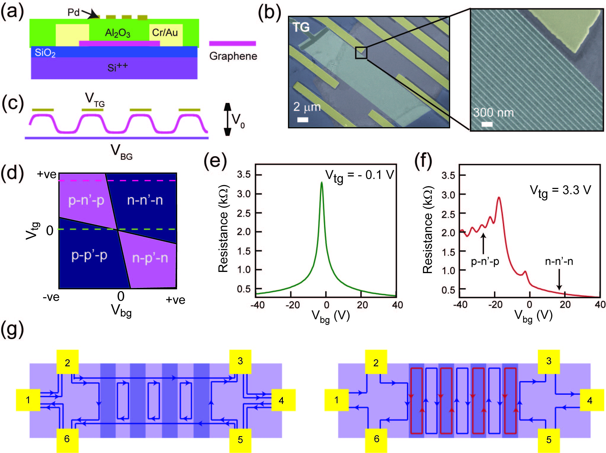
The resistance depends on the filling factor in the adjacent regions Abanin and Levitov (2007); Williams et al. (2007); Özyilmaz et al. (2007); Ki and Lee (2009). At a constant magnetic field B, the filling factor in the adjacent regions is determined by and . Depending on and at a given , we have same type of edge states in the unipolar region, and in the bipolar region, electron and hole edge states co-propagate along the junction (Figure 1(g)). In this device, we have 37 top-gates. So, if the edge states are formed under all the top-gates and they equilibrate along all the edges of the top-gates, then the four-probe resistance () plateau is given by
where is the number of top-gates which is 37 in our device. (Landau-Büttiker formalism to obtain for multiple top-gates in Section V of Supplemental Material.)
Figure 2(a) shows the colorscale plot of zero bias four-probe resistance as a function of and at 14 T. We observe diamond shaped regions in the parameter space that represent integer filling factors in adjacent regions set by and . The filling factors in the two alternating regions are indicated as (,). Figure 2(b, c) show line slices of as function of at 2, 6. (Line slices at 10 and 14 are presented in Section IV of Supplemental Material.) We do not observe large resistance as predicted by Equation I and II. The is relatively high, and does not show a plateau, in the bipolar regime, but not as high as predicted by Equation II.
In the line slices (Figure 2(b, c)), the green curve is the experimental data. The black dashed lines correspond to the calculated plateau for 1 in Equation I and II. We find that in the unipolar regime, denoted by the blue region in Figure 1(d), the potential is small and the plateaus are well described by ; there is good agreement between measured experimental data and expected plateau values for a single top-gate in Figure 2(b,c).
Our experimental observation show plateaus corresponding to a single top-gate and not 37 top-gate, and so we do not have equilibration in our device inside the superlattice. The equilibration occurs only at the extreme edge of the top-gates near the voltage probes as illustrated in the schematic in Figure 2(d). In the schematic, the yellow probes are the real probes and the gray probes are the virtual probes denoting equilibration at that edge. The virtual voltage probes are used to calculate resistance using Landauer-Büttiker formalism Büttiker (1988). One possible reason for the lack of equilibration is that the edge states under the top-gate are defined electrostatically, where the potential varies smoothly due to the finite thickness of the top-gate dielectric Amet et al. (2014). Equilibration requires inter edge state scattering or ohmic contacts so that all the edge states are at the same chemical potential, and this does not happen due to the short length along the physical edge of graphene Kane and Fisher (1995); Alphenaar et al. (1991); Ensslin (2003); Haug (1993).
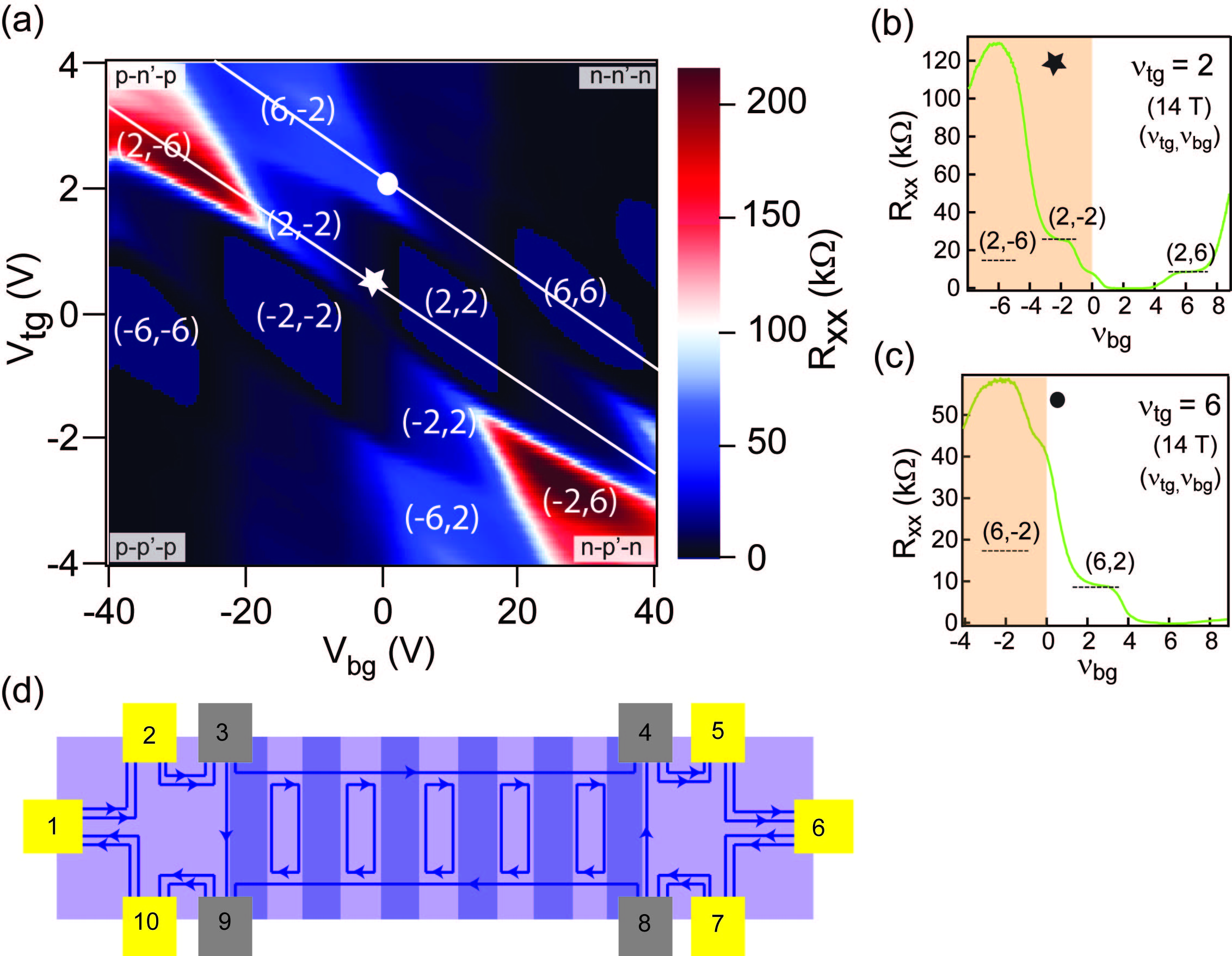
In the bipolar region, plateau coincides with that expected for a single top-gate when 2(-2) and -2(2). When we have one edge state for both electrons and holes circulating in adjacent regions, the resistance plateau is seen at (25.8 k). The plateau at (,) (2,-2) results not only because the is low in this state compared to any other state in the bipolar region but also because this is a special state where the charge carriers belong to the same LL ( 0) and that the LL gap is maximum between 0 and 1 LL. Narrow TG and BG regions inside the superlattice leads to leaky barrier and transmission of edge states resulting in a plateau corresponding to a single top-gate Müller et al. (1995).
However, when neighboring regions have other edge states, that is, and or is greater than 2, we find resistance significantly larger than (for example, (2,-6) in Figure 2(b), (6,-2) in Figure 2(c)); a feature not generally seen in single p-n’-p junction in the quantum Hall state. The feature of plateaus in corresponding to equilibration for a single top-gate in the unipolar region and deviation from this picture in the bipolar region, is quite robust and is also observed in another device with 35 top-gates (details in Section X of Supplemental Material).
The large resistance with maximum 200 k at 14 T, is seen along the diagonal direction in Figure 2(a); it is precisely in this diagonal direction of the parameter space that increases. In the bipolar region, though the value of is higher than that for a single top-gate, it is not 37 times the value for a single top-gate, and thus there is no full equilibration. In this region the array of top-gates does not behave as a single top-gate. The resistance value depends on the gate voltages and the magnetic field, implying that the equilibration can be modified by electric field.
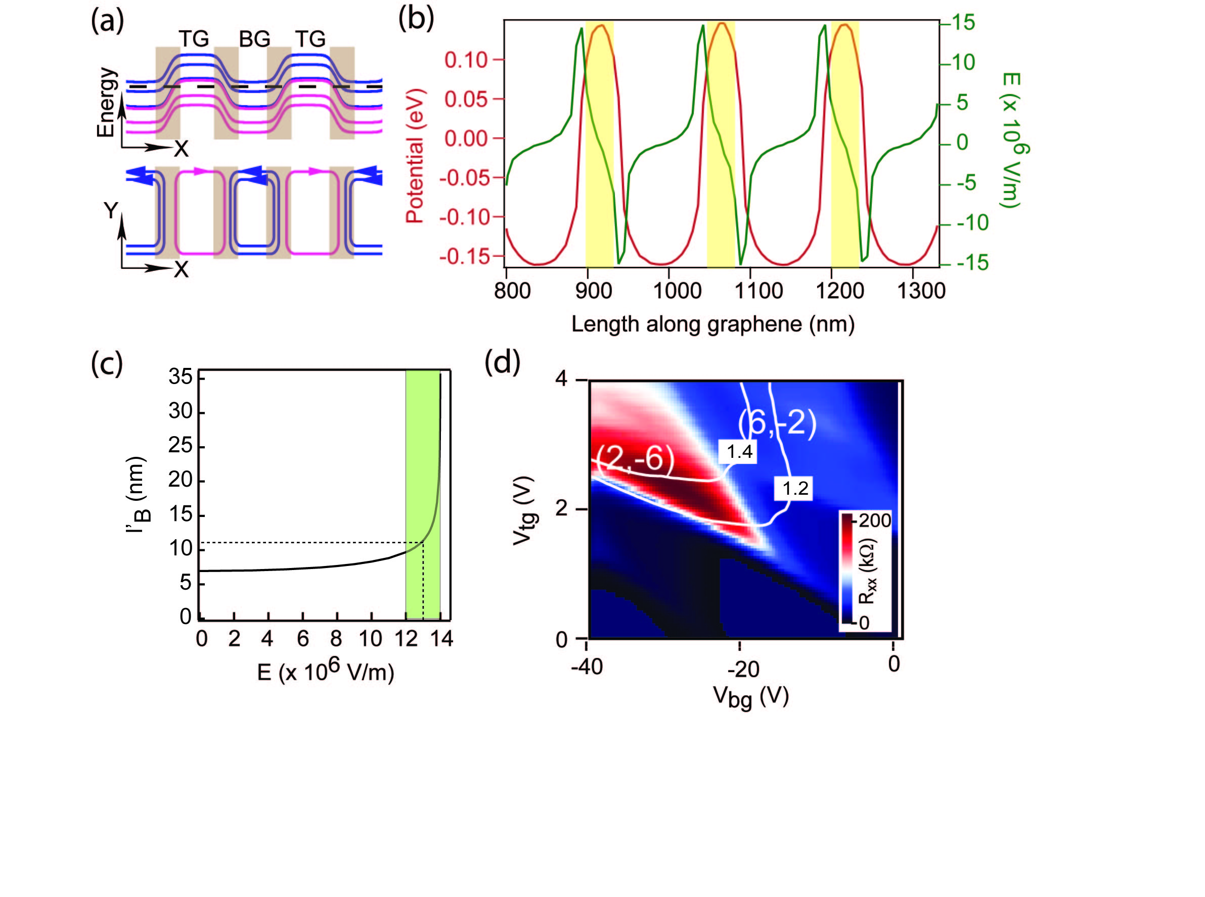
We now try to understand the reason for this observation and note that is relatively large in this region. Figure 3(a) shows a LL diagram along the length of the device when ; where we have co-propagating electron and hole edge states at the junction. At the interface of these regions (shaded brown in Figure 3(a)) there is an electric field (), due to the SL, and it has a significant effect on the LL wavefunctions.
To get an accurate idea of the magnitude of in our devices we performed numerical simulation of the electrostatics using finite element method. At a given and , the charge carrier density induced along the length of graphene is calculated, from which potential and is obtained. (Details of calculation in Section VII of Supplemental Material.) Spatial variation of potential and along length of graphene in bipolar region is shown in Figure 3(b). At a given and , the maximum is obtained which is higher in the bipolar region compared to the unipolar region.
We note that in the bipolar regime, created is much larger than . Large leads to large in the region between BG and TG region which modifies the LLs locally. It has been shown by Lukose et al. Lukose et al. (2007) and later extended by Gu et al. Gu et al. (2011) for the case of a top-gate geometry that the LL spectrum and the wavefunctions in crossed and are fundamentally modified in graphene, an aspect that is not observable in conventional 2DEGS semiconductors. LL wavefunction is modified in two ways. Effective magnetic length in the presence of can be written as Lukose et al. (2007). increases with increasing and rises rapidly when approaches as seen in Figure 3(c). Secondly, the mixes the Landau levels.
Contours of maximum at 1.2107 Vm and 1.4107 Vm are overlaid on the measured data at 14 T as shown in Figure 3(d). Figure 3(d) shows that the contours lie along the region where we have high resistance state and departure from the value for a single top-gate. We argue that in our device geometry, created is high enough to modify LLs which is reflected in charge transport measurements. The spatial extent of the wavefunction () increases with increasing and approaches the width of TG (or BG) region. This leads to increased spatial overlap of the wavefunction within TG (or BG) region of the superlattice resulting in enhanced scattering. Secondly, as function of , there is LL mixing Lukose et al. (2007) which results in a non zero matrix element essential to cause scattering and equilibration. Let us now examine the various lengthscales of our system that support this scenario. From Figure 3(b) we find that the effective electrostatic width of the top-gate for this configuration is 50 nm and the extent of the region with high electric field (between 1.2 - 1.4107 Vm) is 15 nm. In addition, the magnetic length in the presence of transverse electric in this region is 11 nm (see Figure 3(c)). If one considers the scenario of (6,-2) state, we find that with three edge states with width 11 nm will have significant overlap with two adjacent regions and equilibration will be enhanced due to scattering.
In the presence of high electric field, the resistance depends on and applied. For example, resistance values at (,) (6,-2) and (2,-6) at 14 T are different as the maximum is different in the two regions (Plot of maximum as a function of gate voltages in Section VII of Supplemental Material) — this strongly suggests electric field tuning of equilibration.
We think disorder does not play an important role. Because, in our sample, the disorder potential, estimated from the FWHM of the Dirac peak, is 71 meV Dubey et al. (2013), and thus is smaller than in the bipolar region. So, the tuning of equilibration of edge states in our sample, which is seen at higher , is due to the at the interface of TG and BG regions. However, recent work of Kumada et al suggests that the disorder along the length of p-n junction could play an important role in equilibration Kumada et al. (2015); Long et al. (2008). Further experimental and theoretical studies need to be carried out to probe the role of disorder in periodically modulated structures.
Details of LL modification in unipolar region at lower of 3.5 T in Section IX of Supplemental Material.
Our experiments with tunable superlattices suggest that tuning of the equilibration of edge states in graphene can be done using at interfaces, which cannot be realized in conventional 2DEGS. In addition, the nature of the state that emerges after the collapse of the LLs is little understood and possibility of existence of correlations has been speculated Lukose et al. (2007); Carmier et al. (2011). The close proximity of co-propagating electron and hole edge states can be used to construct large class of topological states Sagi and Oreg (2014) and also offers an opportunity to study excitonic effects, this has been recently explored in bilayer quantum Hall systems Nandi et al. (2012). There have been predictions of correlated states in 0 LL of graphene and LL mixing can enable exploration of such phases Kharitonov (2012).
We thank Marcin Mucha-Kruczyński, G.Baskaran, R.Shankar, Jainendra Jain, Vibhor Singh, Shamashis Sengupta and K.Sengupta for discussions and comments on the manuscript. We acknowledge Swarnajayanthi Fellowship of Department of Science and Technology and Department of Atomic Energy of Government of India for support.
References
- Müller et al. (1995) G. Müller, D. Weiss, K. von Klitzing, P. Středa, and G. Weimann, Physical Review B 51, 10236 (1995).
- Tornow et al. (1996) M. Tornow, D. Weiss, A. Manolescu, R. Menne, K. v. Klitzing, and G. Weimann, Physical Review B 54, 16397 (1996).
- Ye et al. (1996) P. D. Ye, D. Weiss, R. R. Gerhardts, K. von Klitzing, K. Eberl, and H. Nickel, Surface Science Proceedings of the Eleventh International Conference on the Electronic Properties of Two-Dimensional Systems, 361/362, 337 (1996).
- Stormer et al. (1991) H. L. Stormer, L. N. Pfeiffer, K. W. Baldwin, K. W. West, and J. Spector, Applied Physics Letters 58, 726 (1991).
- Endo et al. (2001) A. Endo, M. Kawamura, S. Katsumoto, and Y. Iye, Physical Review B 63, 113310 (2001).
- Yang et al. (2002) C. L. Yang, J. Zhang, R. R. Du, J. A. Simmons, and J. L. Reno, Physical Review Letters 89, 076801 (2002).
- Castro Neto et al. (2009) A. H. Castro Neto, F. Guinea, N. M. R. Peres, K. S. Novoselov, and A. K. Geim, Reviews of Modern Physics 81, 109 (2009).
- Das Sarma et al. (2011) S. Das Sarma, S. Adam, E. H. Hwang, and E. Rossi, Reviews of Modern Physics 83, 407 (2011).
- Goerbig (2011) M. O. Goerbig, Reviews of Modern Physics 83, 1193 (2011).
- Dean et al. (2013) C. R. Dean, L. Wang, P. Maher, C. Forsythe, F. Ghahari, Y. Gao, J. Katoch, M. Ishigami, P. Moon, M. Koshino, T. Taniguchi, K. Watanabe, K. L. Shepard, J. Hone, and P. Kim, Nature 497, 598 (2013).
- Ponomarenko et al. (2013) L. A. Ponomarenko, R. V. Gorbachev, G. L. Yu, D. C. Elias, R. Jalil, A. A. Patel, A. Mishchenko, A. S. Mayorov, C. R. Woods, J. R. Wallbank, M. Mucha-Kruczynski, B. A. Piot, M. Potemski, I. V. Grigorieva, K. S. Novoselov, F. Guinea, V. I. Fal’ko, and A. K. Geim, Nature 497, 594 (2013).
- Hunt et al. (2013) B. Hunt, J. D. Sanchez-Yamagishi, A. F. Young, M. Yankowitz, B. J. LeRoy, K. Watanabe, T. Taniguchi, P. Moon, M. Koshino, P. Jarillo-Herrero, and R. C. Ashoori, Science 340, 1427 (2013).
- Dubey et al. (2013) S. Dubey, V. Singh, A. K. Bhat, P. Parikh, S. Grover, R. Sensarma, V. Tripathi, K. Sengupta, and M. M. Deshmukh, Nano Letters 13, 3990 (2013).
- Kawamura et al. (2001) M. Kawamura, A. Endo, S. Katsumoto, Y. Iye, C. Terakura, and S. Uji, Physica B: Condensed Matter International Conference on High Magnetic Fields in Semiconductors, 298, 48 (2001).
- Killi et al. (2012) M. Killi, S. Wu, and A. Paramekanti, International Journal of Modern Physics B 26, 1242007 (2012).
- Özyilmaz et al. (2007) B. Özyilmaz, P. Jarillo-Herrero, D. Efetov, D. Abanin, L. Levitov, and P. Kim, Physical Review Letters 99, 166804 (2007).
- Ki and Lee (2009) D.-K. Ki and H.-J. Lee, Physical Review B 79, 195327 (2009).
- Gu et al. (2011) N. Gu, M. Rudner, A. Young, P. Kim, and L. Levitov, Physical Review Letters 106, 066601 (2011).
- Tikhonenko et al. (2008) F. V. Tikhonenko, D. W. Horsell, R. V. Gorbachev, and A. K. Savchenko, Physical Review Letters 100, 056802 (2008).
- Abanin and Levitov (2007) D. A. Abanin and L. S. Levitov, Science 317, 641 (2007).
- Williams et al. (2007) J. R. Williams, L. DiCarlo, and C. M. Marcus, Science 317, 638 (2007).
- Büttiker (1988) M. Büttiker, Physical Review B 38, 9375 (1988).
- Amet et al. (2014) F. Amet, J. Williams, K. Watanabe, T. Taniguchi, and D. Goldhaber-Gordon, Physical Review Letters 112, 196601 (2014).
- Kane and Fisher (1995) C. L. Kane and M. P. A. Fisher, Physical Review B 52, 17393 (1995).
- Alphenaar et al. (1991) B. W. Alphenaar, P. L. McEuen, R. G. Wheeler, and R. N. Sacks, Physica B: Condensed Matter Analogies in Optics and Micro-Electronics, 175, 235 (1991).
- Ensslin (2003) K. Ensslin, Superlattices and Microstructures 33, 425 (2003).
- Haug (1993) R. J. Haug, Semiconductor science and technology 8, 131 (1993).
- Lukose et al. (2007) V. Lukose, R. Shankar, and G. Baskaran, Physical Review Letters 98, 116802 (2007).
- Kumada et al. (2015) N. Kumada, F. D. Parmentier, H. Hibino, D. C. Glattli, and P. Roulleau, Nature Communications 6, 8068 (2015).
- Long et al. (2008) W. Long, Q.-f. Sun, and J. Wang, Physical Review Letters 101, 166806 (2008).
- Carmier et al. (2011) P. Carmier, C. Lewenkopf, and D. Ullmo, Physical Review B 84, 195428 (2011).
- Sagi and Oreg (2014) E. Sagi and Y. Oreg, Physical Review B 90, 201102(R) (2014).
- Nandi et al. (2012) D. Nandi, A. D. K. Finck, J. P. Eisenstein, L. N. Pfeiffer, and K. W. West, Nature 488, 481 (2012).
- Kharitonov (2012) M. Kharitonov, Physical Review B 85, 155439 (2012).
See pages ,,1,,2,,3,,4,,5,,6,,7,,8,,9,,10,,11,,12,,13,,14,,15 of Supplemental_quantum_Hall_Sudipta.pdf