Highly sensitive gas and temperature sensor based on conductance modulation in graphene with multiple magnetic barriers
Abstract
The electronic and transport properties of graphene modulated by magnetic barrier arrays are derived for finite temperature. Prominent conductance gaps, originating from quantum interference effects are found in the periodic array case. When a structural defect is inserted in the array, sharp defect modes of high conductance appear within the conductance gaps. These modes can be shifted by local doping in the defect region resulting into sensing of the chemical molecules that adhere on the graphene sheet. In general it is found that sensitivity is strongly dependent on temperature due to smoothing out of the defect-induced peaks and transport gaps. This temperature dependence, however, offers the added capability for sub-mK temperature sensing resolution, and thus an opportunity towards ultra-sensitive combined electrochemical-calorimetric sensing.
I Introduction
Advances in fabrication techniques since the isolation of monolayer grapheneNovoselov2004 have allowed the realization of a variety of graphene-based applicationsNovoselov2012 ; Ferrari2015Nanoscale . In terms of electronic applications, graphene’s high carrier mobilityBolotin2008 ; Mayorov2011 has enabled its application as an electrical conducting channelLi2008 ; Geim2009 ; Schwierz2010 , however, the lack of strong conductance modulationWilliams2007 due to Klein tunnelingKlein1929 ; Cheianov2006 ; Katsnelson2006 has limited its utilization for other graphene-based electronic devices. The modulation of charge carriers in graphene is still a significant issue of ongoing research for graphene nanoelectronicsMoriya2014 ; Shih2014 .
A conductance modulation in graphene can be introduced by utilizing various mechanisms that open an electronic band gap, such as the interaction with susbtratesGiovannetti2007 ; Usachov2010 ; Decker2011 ; Bokdam2011 , elastic strainNi2008 ; Shemella2009 ; Kim2009 , or finite-size effects in graphene nanoribbonsHan2007 ; Baringhaus2014 . Aside from the band gap opening, however, these methods also introduce unavoidable disorders, such as charge impurities or structural imperfections by substratesAndo2006 ; Fratini2008 ; Chen2008 ; Katsnelson2007 and strong backscattering by rough edges of graphene nanoribbonsFang2008 ; Wang2008 ; Mocciolo2009 , that deteriorate the transport properties of graphene. An alternative mechanism for band-gap opening, that in principle does not produce any disorder effects in graphene, is the use of inhomogeneous magnetic fields. Particularly, since inhomogeneous magnetic fields can tune the Dirac fermion transport in graphene mimicking a typical potential barrier for Dirac fermionsRamenzaniMasir2008 ; Ghosh2009 , one can produce magnetic confinement effects for graphene carriersDeMartino2007 ; Myoung2011a . These effects have motivated research on various structures, e.g., magnetically defined quantum dotsDeMartino2007 ; Schnez2008 , Dirac fermion waveguidesMyoung2011a ; Ghosh2008 , and superlatticesWu2008 ; DellAnna2009 .
Besides nanoelectronics, another important aspect of graphene applications is gas sensingBarbolina2006 ; Schedin2007 . The operation principle of a graphene gas sensor relies on measuring the modulated transport properties of graphene that are induced by the adhesion of gas molecules on the graphene surface. In particular, conductance changes arise from the injection of charged carriers into graphene from adhered gas molecules such as O2, NO2 or NH3, which play roles of electron donors or acceptorsOhta2006 ; Schedin2007 ; Zhou2008 . It has been shown that highly sensitive graphene-based gas sensing capable of detecting individual molecule adhesionSchedin2007 is possible, but a large array of sensors might still be required in order to enlarge the exposed area of graphene and thus increase the chances for molecule adhesion at shot-time exposures and minute concentrations. Alternatively, here we explore ways of increasing the minimum exposed area required for single molecule detection without making arrays, which is significant for minimizing device sizes and detection speeds.
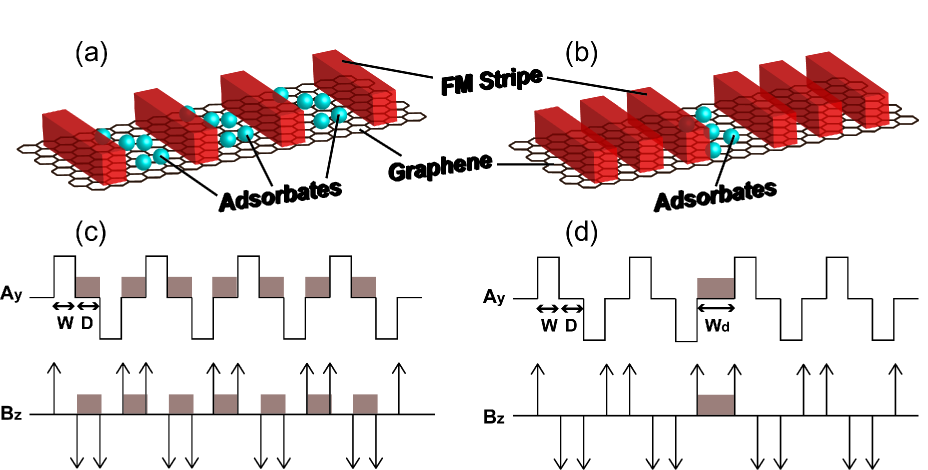
Here, we theoretically study an alternative possibility for achieving highly sensitive gas sensing, which is to utilize the adsorbate-induced electrochemical doping effects in order to modulate the tunneling resonances (TR) and transport band gaps (TBG) emerging in magnetic barrier arrays in graphene. We show that in such graphene sensors the presence of adsorbates introduces strong changes into graphene’s electrical conductance. We take into account two structures for the conductance modulation, as illustrated by Fig. 1. First, we consider a periodic array of magnetic barriers in which the inter-barrier regions are exposed to electrochemical adsorbates. In the second case, we consider a periodic magnetic barrier array with a structural defect, where electrochemical doping is induced only in the defect region. We investigate the ballistic conductance and its modulation by doping effects for both structures, in different temperature ranges. Specifically, in the zero-temperature limit, the presence of a structural defect leads to sharp resonance peaks in the conductance spectra, that can be sensitively modulated by local doping in the defect region. In finite-temperature cases, on the other hand, the overall sensitivity is reduced because of thermal smoothing, but still remains significant within the transport band gaps when a periodic magnetic barrier array with electrochemical doping in-between the barriers is considered. By the same token, however, the strong temperature dependence which is regarded as a weak point in terms of gas sensing, can be used for temperature sensing. The highest sensing ability is expected at lower temperatures, and yields a promising sensing platform for applications in a low-temperature environment.
This manuscript is organized in the following manner: in Sec. II, we present the model Hamiltonian employed to represent multiple magnetic barriers, and we explain the transfer matrix formalism which is valid in the ballistic regime at finite temperatures. In Sec. III, we discuss the features of the defect-induced tunneling resonances in the transmission spectra. Next, in Sec. IV we show the calculated results for the sensing effect by local doping in the zero-temperature limit, and in Sec. V we discuss the large conductance modulation beyond the zero-temperature limit and its temperature dependence. Finally, section VI contains the conclusions and a summary of our results.
II Model Hamiltonian and Formalism
We consider a graphene sheet with a periodic array of magnetic barriers. Magnetic barriers have been experimentally realized by ferromagnetic stripes on top of a graphene sheetCerchez2007 . To describe Dirac fermion ballistic transport through the system we will use the transfer matrix formalism. Starting with the simplest case of a single magnetic barrier along the -direction, the Dirac Hamiltonian readsMyoung2009
| (1) |
where m/s is the Fermi velocity of Dirac fermions, and are Pauli matrices acting on sublattices of graphene. For simplicity, the magnetic barrier is characterized by a rectangular profile of the vector potential:
| (2) |
where is the magnetic field strength, the characteristic magnetic length, is the Heaviside step function and is the width of the magnetic barrier. The corresponding magnetic fields are given by , which corresponds to delta-function-like spikes of opposite sign at the two edges of the magnetic barrier. A general expression of the solution in the three different regions , and is written as Myoung2009 :
| (7) |
where or represents different regions. The solution can be written in the matrix form:
| (10) |
with the matrices and defined as:
| (13) | ||||
| (16) |
where
| (17) |
We take into account the low-lying excitation of Dirac fermions in graphene, below meV from the charge neutral point, in order to remain within the linear-band approximation governed by the Dirac equation. The magnetic barrier height is found from the definition of at normal incidence to be . To avoid having negligible tunneling of Dirac fermions through the magnetic barrier, the magnetic barrier width should not exceed a few tens nm. Additionally, the total lateral size of a multiple magnetic barrier array should not be over a few microns so we could still be in ballistic transport regime even at room-temperaturesMayorov2008 .
In order to obtain the transmission and reflection probabilities through a single magnetic barrier, we calculate the undetermined coefficients and through the application of the boundary conditions, i.e. that wavefunctions should be continuous at the interfaces and . We note that in this study we do not need to take into account the Zeeman energy , where is the gyromagnetic factor for Dirac fermions in graphene and is the Bohr magneton, because the anti-symmetric magnetic field profiles of each single magnetic barrier yield no spin-dependent transport phenomenaMyoung2011b . The wavefunction continuity provides the following equations:
| (22) | ||||
| (27) |
By combining these, we get an equation connecting the coefficients the incoming and outgoing solutions:
| (32) |
where is the transfer matrixMcKeller2007 ; Barbier2008 .
| (35) |
Alternatively, the transfer matrix could also be derived using optical analogies, as shown in Appendix A. We note here that since we are interested in ballistic transport of Dirac fermions through the structures, no disorder effects that could lead to energy dissipation by inelastic scattering were included in the our formalism.
The transmission probability is obtained from the transfer matrix by . Note that is not only a function of the energy but also of the incident angle of the incoming Dirac fermions. In the ballistic regime and at finite temperature, the conductance through a two-dimensional system is obtained by the weighted average of the transmission function over the incident angle, in accordance to the Landauer-Büttiker formalismButtiker1985 :
| (36) |
where is the system size in the transverse () direction, is the propagating direction of incoming Dirac fermions, and is Fermi-Dirac distribution with given Fermi energy and temperature . In the zero temperature limit the conductance formula is simplified to:
| (37) |
Next, we consider a monolayer graphene sheet in the presence of a series of magnetic barriers. The models considered in this study are shown in Fig. 1, where we assume periodically arranged barriers with an inter-barrier distance . Note that we set an alternating configuration of the magnetic barriers, i.e., alternating signs of the vector potentials. The transfer matrix formalism for multiple magnetic barriers can be extended from the case of the single magnetic barrier:
| (38) |
where is the number of magnetic barriers in use, and
| (43) |
where is the position of -th magnetic barrier and is for upward or downward magnetic barriers. In the following sections we assume 20 magnetic barriers periodically arranged with nm, nm, meV and nm.
III Transmission probability through multiple magnetic barriers
In this section, we discuss defect-induced resonances and local-doping effects in the transmission probability of Dirac fermions through multiple magnetic barriers. The existence of defect-induced resonances is best demonstrated by comparing the transmission spectra through a periodic array of magnetic barriers without and with a structural defect, as illustrated in Fig. 1(a) and (b), respectively, and plotted for normal incidence in Fig. 2.
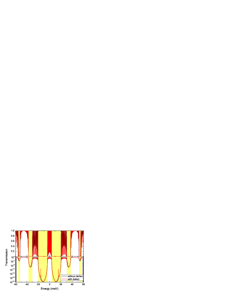
It is shown that the periodic arrangement of magnetic barriers leads to the existence of transport gaps (TG) in specific energy ranges, indicated by shaded regions in Fig. 2. The emergence of TGs comes from the combination of strong back scattering by the magnetic potentials and quantum interference effects in the periodic structure, similarly to the Kronig-Penny model. (The existence of the TG is best understood by the band structure of the infinite magnetic barrier array, shown in Appendix B.) At energies below the magnetic barrier height ( meV), only resonant tunnelings through the multiple magnetic barrier are allowed, with the number of resonances being equal to the number of magnetic barriers. Let us call these resonances for under-barrier tunneling ‘bound-state tunneling resonances’ (BTRs). For the defected magnetic barrier array, on the other hand, sharp transmission peaks emerge in the TGs. We call these ‘defect-induced tunneling resonances’ (DTRs). Due to their positioning within the TGs, a large modulation in transmission probability is expected near their peaks.
We next consider the effect of doping induced by adsorbates on the graphene sheet. In the periodic array case we assume that all the inter-barrier regions are exposed to adsorbates, while in the defected array case we assume local doping applied to the defect region only, as respectively illustrated in Fig. 1(a) and (b). Doping is introduced in our model as a rectangular electrostatic potential barrier, characterized by the barrier height .
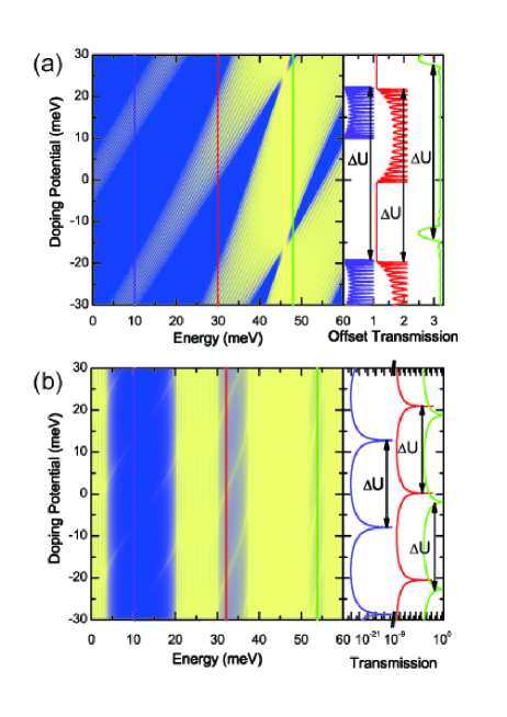
The effects of doping on the transmission probability are shown in Fig. 3. In the case of inter-barrier doping of a periodic array without structural defects, the transmission spectra are entirely shifted by the doping potential. This shift is enough to produce strong qualitative changes in the transmission spectra above the barrier height, e.g. at the specific energy meV, where the TG disappears and the transmission of Dirac fermions is almost unaffected by doping. Local doping in the defect region, on the other hand, does not lead to a global shift of the transmission spectra, but produces a clear shift of the DTRs: the transmission peaks are shifted, and new ones periodically appear as the local doping potential increases.
The periodic nature of the transmission peaks is well interpreted by the quantum phase through the regions where doping potentials are induced. The round-trip phase acquired by Dirac fermions while moving through a distance is given by
| (44) |
At a given energy, the periodicity of the potential energy specific strength that yields can be found. In the particularly simple case of normal incidence, Eq. (44) leads to a universal where for the inter-barrier doping case and for the local doping case. Indeed, for the inter-barrier doping, we find meV, as verified in the inset of Fig. 3(a), while for the local doping the energy interval between the defect-induced transmission peaks is meV, also shown in inset of Fig. 3(b). The same insets show the universality of the doping potential periodicity, being the same for different energies at normal incidence, albeit it will vary according to the incident angle.
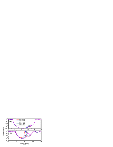
The high sensitivity of the DTRs to small local doping is shown in Fig. 4, in two different energy ranges corresponding to TGs in under- () and over-barrier () tunneling regimes. Owing to their positioning within a TG, DTRs are sufficiently sharp, especially those within the lower energy TG, so that one can expect that the transport properties of graphene can be greatly modified by local doping. Note that a doping strength of meV at meV approximately corresponds to a change in carrier concentration cm-2, which is much smaller than the actual carrier concentration of graphene cm-2 at that Fermi energy. (See Ref. Hwang2007 and reference therein)
IV Conductance Modulation by Doping at Zero Temperature
We studied in the previous section the transmission probabilities of Dirac fermions through periodic magnetic barrier structures in the presence or absence of structural defects, and found that slight shifts of the defect-induced resonant peaks can produce significant changes to the transmission probability. In this section, we calculate the zero temperature ballistic conductance through a graphene sheet decorated with magnetic barrier arrays and its dependence on doping, with particular focus on the DTR shifts.
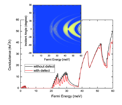
In the zero-temperature limit, conductance is calculated from Eq. (37), which we plot in Fig. 5. Similarly to the transmission spectra, defect-induced peaks that are modulated by local doping appear within the transport dips of the conductance curve. There is, however, an important difference: the conductance no longer drops to low values, especially at higher energies. At low energy, on the other hand, the conductance is dominated by under-barrier tunneling through the barriers, resulting into a complete TG within which the conductance values almost vanish. The complete gap in low energy is due to the strong backscattering of the magnetic barriers, while the incomplete dips in high energies originate from the quantum interference effects in the periodic array of magnetic barriers. The nature of the two transport regimes is further revealed by the symmetry of the conductance resonances as shown in the inset in Fig. 5 in connection to Eq. (37): the isotropic backscattering from the alternating magnetic barriers in the low-energy under-barrier tunneling regime reflects a complete transport gap, while the strong dependence on the incident angle of the high-energy over-barrier tunneling of Dirac fermions reflects the incomplete drop of conductance values.
With the possibility of a sensing application, it is necessary to have a figure of merit for the conductance sensitivity to doping. To this end, we introduce gauge factors () as commonly used for characterizing sensing performance:
| (45) |
where is the graphene resistance and the local carrier concentration as a consequence of the local doping. These two different definitions of the gauge factor can be selectively applied to specify the sensitivity, according to the way of measuring the transport properties of graphene.
IV.1 Effects of doping on the ballistic conductance without a defect
For a periodic array of magnetic barriers, the ballistic conductance calculated by Eq. (37) and its dependence on the inter-barrier doping are displayed in Fig. 6(a). The conductance curves are entirely shifted as the doping potential varies. Figures 6(b) and (c) present the gauge factors and , i.e. the sensitivity of the conductance modulation by the inter-barrier doping, for various doping potentials. As expected, the exhibits an opposite dependence on the doping potential compared to , according to their definition (see Eq. (45)). Since the inter-barrier doping effects lead to the entire shift of the conductance, very sensitive changes in the conductance value are obtained around the BTRs and the complete TG edges in the under-barrier tunneling regime. A large gauge factor is obtained near the TG edge meV, resulting into for , i.e. assuming a resistance variation as the measurement resolution. Even higher gauge factor is obtained in the low energy edge at meV. In other words, such a large value of the gauge factor means that the detection of the single free carrier injection/extraction is possible within area exposed to electrochemical adhesion for . In the over-barrier regime, on the other hand, the sensitivity of the conductance modulation by the inter-barrier doping is expected to be much less sensitive, compared to the under-barrier regime.
IV.2 Sensitivity of the conductance modulation with a defect: under-barrier versus over-barrier
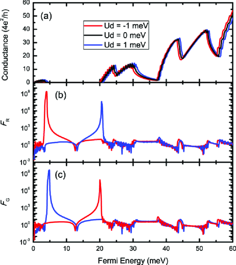
Next, we discuss the effects of local doping on the DTRs. In Figs. 7(a) and (c), the local-doping dependence of the conductance is shown in the under-barrier and over-barrier tunneling regimes, respectively, exhibiting shifts similarly to the transmission peaks at normal incidence. Despite the small change in the doping potential ( meV), the separation of the shifted peaks are enough to produce a significant amount of conductance modulation, offering a scheme for sensitive adsorbate detection.
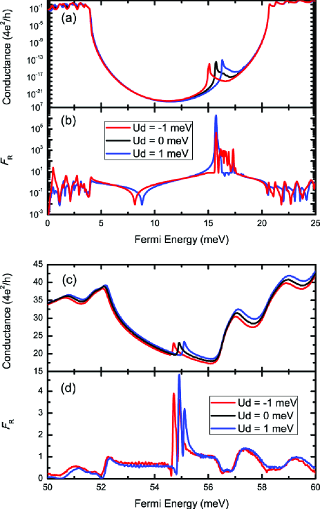
In the under-barrier tunneling regime, Fig. 7(a) exhibits a large contrast in the conductance values around DTRs. One can expect that the conductance abruptly decreases with small amount of doping because of the sharpness of the conductance peak in this regime. This ultra-sensitive conductance modulation allows us to obtain a very large value of the gauge factor, up to as displayed in Fig. 7(b), but the actual magnitude of the conductance in this regime is too small.
On the other hand, in the over-barrier tunneling regime, Fig. 7(c) exhibits that the conductance values are greater than those in the under-barrier regime and there are DTRs within the conductance dip. The DTRs are shifted by the local doping effects as well, but the gauge factor in the over-barrier regime is expected to be much smaller, compared to those in the under-barrier tunneling regime, as shown in Fig. 7(d), due to the incomplete conductance drop, and thus small contrast, around the DTRs. Here, we note that for simplicity we show only, since maximum values of are also found near the DTRs and as expected are almost the same as those of .
IV.3 Enhancement of the sensitivity by collimators
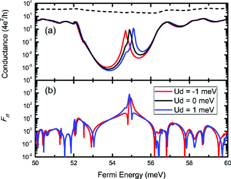
The incomplete conductance drop in the over-barrier regime is attributed to the transport contributions coming from all incident angles of Dirac fermions. If these angular contributions could be suppressed, the transport dips will get deeper, resulting into a larger contrast near the DTRs. To this end, we propose the use of a Dirac fermion collimator to kill the non-zero incident angle contributions to the conductance. In particular, it has been known even a single electrostatic barrier can produce a collimation effectPark2008 ; Barbier2010 . This is easily seen in the first of Eq. (17), where for any non-zero value of results into an imaginary , and thus into suppressed transmission. The normal incidence transmission, on the other hand, remains always protected by Klein tunneling. In our model, we thus introduce an electrostatic barrier of potential height and barrier width nm at both sides of the magnetic barrier array. This leads to the suppression of all non-zero angular contributions to the conductance near , and thus to an increase of the conductance contrast around it.
Figure 8 shows the effects of a collimator with potential height set to match the energy corresponding to a DTR. Indeed, the transmission dip becomes deeper in the presence of the collimator, increasing the conductance contrast, and thus becomes large up to . Such a gauge factor enables the detection of , for . As experimentally demonstratedSchedin2007 , the exposure of a graphene sheet to 1 NO2 gas results into cm-2 with few of resistance changes. With the same order of magnitude of , is expected to be detected. Therefore, our results offer an opportunity for sub- level detection of gas molecules by using the doping-induced shift of DTRs. However, this is still much lower than the sensitivity offered by the periodic array shown in the previous subsection, because of the still relatively large background conductance around the DTR, despite the use of the collimator. In closing this section, we remind that the application of the collimator to the under-barrier regime would not be useful because complete TGs already exist there.
V Conductance Modulation by Doping Effects at Finite Temperature
Our discussion regarding the conductance modulation has done in the zero-temperature limit. It is necessary, however, to also know up to what extend our results will be valid for the more practical cases of finite temperature. In this section, we investigate the finite-temperature effects on the ballistic transport through the two types of multiple magnetic barrier structures and examine the conductance modulation by doping based on Eq. (36).
V.1 Temperature effects on the conductance through periodic magnetic barriers
We consider the periodic array of magnetic barriers with all inter-barrier regions exposed to electrochemical dopants (see Fig. 1(a)).
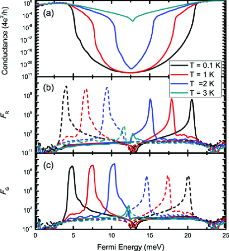
In the previous section, we found that the conductance modulation for the periodic magnetic barriers is expected to be significant around the edges of the complete TGs which correspond to the under-barrier tunneling. The calculated conductance modulation and the corresponding sensitivity are depicted in Fig. 9, showing their temperature dependence. At K, large values of the gauge factor are observed near the TG edge, similarly with the results in the zero-temperature limit. This gauge factor peaks are due to the fact that the conductance values abruptly increase near the TG edges with a small . As temperature increases, the gauge factor peak is shifted to the center of the TG, exhibiting minor reduction in the sensitivity up to K. This shift of the gauge factor peak means that the variation of the conductance values near the TG edge becomes smoother as temperature increases. The sensitivity is dramatically reduced at K, so that the sensitive detection of the presence of the adsorbates in-between magnetic barriers is valid for the low-temperature limit below K.
V.2 Temperature effects on defect-induced tunneling resonances
As discussed, the key feature of highly sensitive conductance modulation in the defected array case results from the existence of DTRs and their shift by doping. In order to consider the possibility for finite-temperature gas sensing, it is necessary to see whether the DTRs survive at finite temperatures.
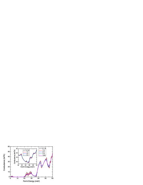
Figure 10 displays the ballistic conductance through multiple magnetic barriers with a defect as a function of fermi energy for several temperatures. At low temperature K, the distinct DTRs are clearly observed within the transporting dips, similar to the zero-temperature limit. As temperature increases, however, the DTRs, which are responsible for the high sensitivity to the doping, become smoothed out. Thus, it is not expected to achieve high sensitivity with this system at finite temperatures.
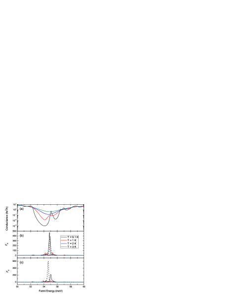
Indeed, the sensitivity of the conductance modulation near the DTR severely diminishes as temperature increases, as shown in Fig. 11(a). At low temperature K, the doping dependence of the conductance still exhibits an apparent DTR within the conductance drop, similarly to the zero-temperature limit. The maximum value of gives , corresponding to a sensitivity reduction of a factor of 2 compared to the zero-temperature case. Despite this reduction, it is still enough for sub- level gas detection as aforementioned. However, as temperature increases, the DTRs becomes completely smoothed out, eliminating any sensitivity, as seen in Fig. 11(b) and (c). Therefore, one can only expect highly sensitive detection of local doping at the low-temperature limit below K. We note here, that the larger gauge factor values are achieved for negative doping potentials because of the asymmetric profile of the DTRs.
V.3 Sensitive detection of temperature variation
We have found profound deductions of the gauge factors at finite temperatures/ However, while this is a limitation for gas sensing, such a severe temperature dependence may become an asset which allows us to detect minute temperature changes.
In order to characterize the temperature sensing ability, we define the following gauge factors with respect to temperature changes:
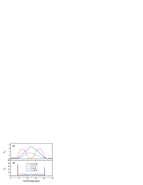
| (46) |
where is the change in temperature. Similar to or , and imply how sensitively the conductance is modulated as temperature changes. Figure 12 shows the calculated gauge factors as a function of Fermi energy in the under-barrier tunneling regime. It is clearly seen that is suitable for the temperature sensing. Large values of are achieved near the TG edge and the BTRs at low temperature K. As temperature increases, the sharp and large gauge factor peaks are reduced and shifted to the center of the TG because the TG becomes narrower and shallower by temperature, as we aforementioned.
At specific temperatures, the detection of temperature change is determined by and , as . For example, at K, a can be found, which for conductance measurement resolution results into sub-mK level temperature detection. Obviously, the sensitivity of the temperature detection becomes reduced at higher temperature, but the expected is still small below 1 K, assuming . Therefore, the strong temperature-dependent behavior of the ballistic conductance, which reduces the potential for adsorbate detection, can be used for temperature sensing effects.
VI Summary
This article assesses how the ballistic conductance through multiple magnetic barriers is modulated by local doping induced via electrochemical adsorbates on graphene surface. Both periodic and defected barrier arrays were studied. In the zero-temperature limit, large sensitivity to electrochemical doping with single molecule detection was found at the edges of the transport gaps in the periodic case under inter-barrier doping, while sub-p.p.m sensitivity was found on the defect-induced peaks of the defected barrier array for local doping in the defect area only. In the latter case, the use of a Dirac fermion beam collimator (i.e. a suitable electric potential barrier) to suppress transport of Dirac fermions with non-zero incident angles was found to be necessary.
The sensitivity of the conductance modulation is also discussed in the finite-temperature case. The defect-induced transport resonances (DTR) within the conductance gaps are smoothed out as temperature increases, even around 1 K, and so that the sensitivity of the conductance modulation becomes much less than that in the zero-temperature limit. In the case of periodic barriers with inter-barrier doping in the under-barrier tunneling regime, large values of the sensitivity gauge factors can still be found below 3 K, however, as temperature increases beyond 3 K, the gauge factors drastically decreases because of the thermal smoothing. Interestingly, this strong temperature dependence of the sensitivity is advantageous in terms of temperature sensing effects, allowing sub-K level temperature detection. This temperature sensing capability is found to increase as temperature decreases towards zero, pointing towards a temperature sensor that could be particularly useful in low-temperature experiments, outer space, etc. Furthermore, the combination of the strong temperature dependence with the low thermal capacitance of the electron gas, may be an excellent platform for extremely sensitive calorimetric studies involving energy transfer between adsorbates, optical transitions, relaxation precesses, etc, in low-temperature experiments.
Acknowledgements.
We acknowledge funding from EU Graphene Flagship (no. 604391).References
- (1) K. S. Novoselov, A. K. Geim, S. V. Morozov, D. Jiang, Y. Zhang, S. V. Dubonos, I. V. Grigorieva, and A. A. Firsov, Science 306, 666 (2004).
- (2) K. S. Novoselov, V. I. Fal’ko, L. Colombo, P. R. Gellert, M. G. Schwab, and K. Kim, Nature (London) 490, 192 (2012).
- (3) A. C. Ferrari et al., Nanoscale 7, 4598 (2015).
- (4) K. I. Bolotin, K. Sikes, Z. Jiang, M. Klima, G. Fudenberg, J. Hone, P. Kim, and H. Stormer, Solid State Commun. 146, 351 (2008).
- (5) A. S. Mayorov, R. V. Gorbachev, S. V. Morozov, L. Britnell, R. Jalil, L. A. Prnomarenko, P. Blake, K. S. Novoselov, K. Watenabe, T. Taniguchi, and A. K. Geim, Nano. Lett. 11, 2396 (2011).
- (6) , X. Li, G. Zhang, X. Bai, X. Sun, X. Wang, E. Wang, and H. Dai, Nat. Nanotechnol. 3, 538 (2008).
- (7) A. K. Geim, Science 324, 1530 (2009).
- (8) F. Schwierz, Nat. Nanotechnol. 5, 487 (2010).
- (9) J. R. Williams, L. DiCarlo, and C. M. Marcus, Science 317, 638 (2007).
- (10) O. Klein, Z. Phys. 53, 157 (1929).
- (11) V. V. Cheianov and V. I. Falko, Phys. Rev. B 74, 041403(R) (2006).
- (12) M. I. Katsnelson, K. S. Novoselov, and A. K. Geim, Nat. Phys. 2, 620 (2006).
- (13) R. Moriya, T. Tamaguchi, Y. Inoue, S. Morikawa, Y. Sata, S. Masubuchi, and T. Machida, Appl. Phys. Lett. 105, 083119 (2014).
- (14) S.-J. Shih, Q. H. Wang, Y. Son, X. Jin, D. Blankschtein, and M. S. Strano, ACS Nano 8, 5790 (2014).
- (15) G. Giovannetti, P. A. Khomyakov, G. Brocks, P. J. Kelly, and J. van den Brink, Phys. Rev. B 76, 073103 (2007).
- (16) D. Usachov, V. K. Adamchuk, D. Haberer, A. Grueneis, H. Sachdev, A. B. Praobrajenski, C. Laubschat, and D. V. Vyalikh, Phys. Rev. B 82, 075415 (2010).
- (17) R. Decker, Y. Wang, V. W. Brar, W. Regen, H.-Z. Tsai, Q. Wu, W. Gannett, A. Zettl, and M. F. Crommie, Nano Lett. 11, 2291 (2011).
- (18) M. Bokdam, P. A. Khomyakov, G. Brocks, Z. Zhong, and P. J. Kelly, Nano Lett. 11, 4631 (2011).
- (19) Z. H. Ni, T. Yu, Y. H. Lu, Y. Y. Wang, Y. P. Feng, and Z. X. Shen, ACS Nano 2, 2301 (2008).
- (20) P. Shemella and S. K. Nayak, Appl. Phys. Lett. 94, 032101 (2009).
- (21) K. S. Kim, Y. Zhao, H. Jang, S. Y. Lee, J. M. Kim, K. S. Kim, J. H. Ahn, P. Kim, J. Y. Choi, and B. H. Hong, Nature (London) 457, 706 (2009).
- (22) M. Y. Han, B. Ozyilmaz, Y. Zhang, and P. Kim, Phys. Rev. Lett. 98, 206805 (2007).
- (23) J. Baringhaus, M. Ruan, F. Edler, A. Tejeda, M. Sicot, A. Taleb-Ibrahimi, A.-P. Li, Z. Jiang, E. H. Conrad, C. Berger, C. Tegenkamp, and W. A. de Heer, Nature (London) 506, 349 (2014).
- (24) T. Ando, J. Phys. Soc. Jpn. 75, 074716 (2006).
- (25) S. Fratini and F. Guinea, Phys. Rev. B 77, 195415 (2008).
- (26) J.-H. Chen, C. Jang, S. Xiao, M. Ishigami, and M. S. Fuhrer, Nat. Nanotechnol. 3, 206 (2008).
- (27) M. I. Katsnelson and A. K. Geim, Phil. Trans. R. Soc. A 366, 195 (2007).
- (28) T. Fang, A. Konar, H. Xing, and D. Jena, Phys. Rev. B 78, 205403 (2008).
- (29) X. Wang, Y. Ouyang, X. Li, H. Wang, J. Gou, and H. Dai, Phys. Rev. Lett. 100, 206803 (2008).
- (30) E. R. Mocciolo, A. H. Castro Neto, and C. H. Lewenkopf, Phys. Rev. Lett. 79, 075407 (2009).
- (31) M. Ramenzani Masir, P. Vasilopoulos, and F. M. Peeters, Appl. Phys. Lett. 93, 242103 (2008).
- (32) S. Ghosh and M. Sharme, J. Phys.: Condens. Mater. 21, 292204 (2009).
- (33) A. De Martino, L. Dell’Anna, and R. Egger, Phys. Rev. Lett. 98, 066802 (2007).
- (34) N. Myoung, G. Ihm, and S. J. Lee, Phys. Rev. B 83, 113407 (2011).
- (35) S. Schnez, K. Ensslin, M. Sigrist, and T. Ihn, Phys. Rev. B 78, 195427 (2008).
- (36) T. K. Ghosh, A. De Martino, W. Häusler, L. Dell’Anna, and R. Egger, Phys. Rev. B 77, 081404(R) (2008).
- (37) Q.-S. Wu, S.-N. Zhang, and S.-J. Yang, J. Phys.: Condens. Mater. 20, 485210 (2008).
- (38) L. Dell’Anna and A. De Martino, Phys. Rev. B 79, 045420 (2009).
- (39) I. I. Barbolina, K. S. Novoselov, S. V. Morozov, E. W. Hill, P. Blake, M. I. Katsnelson, and K. S. Novoselov, Nat. Mater. 6, 652 (2006).
- (40) F. Schedin, A. K. Gein, S. V. Morozov, E. W. Hill, P. Blake, M. I. Katsnelson, and K. Novoselov, Nat. Mater. 6, 652 (2007).
- (41) T. Ohta, A. Bostwick, T. Seyller, K. Horn, and E. Rosenberg, Science 313, 951 (2006).
- (42) S. Y. Zhou, D. A. Siegel, A. V. Fedorov, and A. Lanzara, Phys. Rev. Lett. 101, 086402 (2008).
- (43) M. Cerchez, S. Hugger, T. Heinzel, and N. Schulz, Phys. Rev. B 75, 035341 (2007).
- (44) N. Myoung and G. Ihm, Physics E, 42, 70 (2009).
- (45) A. S. Mayorov, R. V. Gorbachev, S. V. Morozov, L. Britnell, R. Jalil, L. A. Ponomarenko, P. Blake, K. S. Novoselov, K. Watanabe, T. Taniguchi, and A. K. Geim, Nano Lett. 11, 2396 (2008).
- (46) N. Myoung and G. Ihm, J. Kor. Phys. Soc. 59, 2275 (2011).
- (47) B. H. J. McKeller and C. J. Stephenson, Jr., Phys. Rev. C 35, 2262 (2007).
- (48) M. Barbier, F. M. Peeters, P. Valiopoulos, and J. M. Pereira, Phys. Rev. B 77, 115446 (2008).
- (49) M. Büttiker, Y. Imry, R. Landauer, and S. Pinhas, Phys. Rev. B 31, 6207 (1985).
- (50) E. H. Hwang, S. Adam, and S. Das Sarma, Phys. Rev. Lett. 98, 186806 (2007).
- (51) C.-H. Park, Y. W. Son, L. Yang, M. L. Cohen, and S. H. Louie, Nano Lett. 8, 2920 (2008)
- (52) M. Barbier, P. Vasilipoulos, and F. M. Peeters, Philos. Trans. R. Soc. A 368, 5499 (2010).
Appendix A Optical analogy of the transfer matrix and analytic formalism
For plane-wave solutions, the propagating behavior of Dirac fermions can be governed by an optical analogy. The transfer matrix is also expressed by an alternative representation.
As the starting point, let us consider a boundary between two regions with different potentials. In the left and right sides of the boundary, wavefunctions are given by
| (49) | ||||
| (52) | ||||
| (55) | ||||
| (58) |
as well-interpreted in the main text. These plane-wave solutions must be matched by the wavefunction continuity. The boundary condition leads to the following equation:
| (65) | ||||
| (68) |
where
| (69) |
The ‘interface’ matrix implies scattering effects at the interface when Dirac fermions come from the region 2 to the region 1. Next, we look at the propagation of Dirac fermions through a region where potentials are homogeneously given. The ‘propagation’ matrix is given by
| (72) |
where is the length of -th region.
Now, we can study transmission of Dirac fermions through a potential barrier by using the interface and the propagation matrix:
| (77) | ||||
| (80) |
The matrix corresponds to the transfer matrix that describes the relation between incoming and outgoing waves. The matrix elements are given by
| (81) |
where all parameters , , , , , and are the same as those given in the main text. Also, and are the barrier and the inter-barrier width.
We next formulate the transmission problem:
| (86) |
where and are the reflection and transmission coefficients. Solving this equation, we obtain the following relations between and :
| (87) |
and we finally have:
| (88) |
In order to get , we take the determinant of individual matrices as . It is straightly seen , and the determinant of the interfaces matrices is obtained by
| (89) |
In results, the determinant of the transfer matrix is unity, as expected for a lossless system.
Thus, the reflection and transmission probabilities are calculated as follows:
| (90) |
It is easily found , implying the flux conservation.
We formulate the transfer matrix which has the correspondence to the photonic analogy of multilayer structures. We examine a periodic array of magnetic barriers. In this case, Bloch’s theorem leads to the following expression:
| (97) |
where . We now have the secular equation:
| (100) |
of which diagonalization gives the corresponding eigenstates:
| (101) |
or more conveniently
| (102) |
This transcendental equation gives the band structure at the transport problem.
We can also calculate the transmission probability through N barriers based on the following arguments:
| (109) |
where
| (112) |
In the case that the total flux is conserved, the transmission probability is expressed as below:
| (113) |
Appendix B Band structures for magnetic superlattices
As aforementioned, for an infinite number of magnetic barriers, i.e., magnetic superlattices, the band structures are obtained by
| (114) |
where is the Bloch wavevector and is the period of magnetic superlattices. The band structures of magnetic superlattices reflects transport properties, especially the nature of the transporting gap.
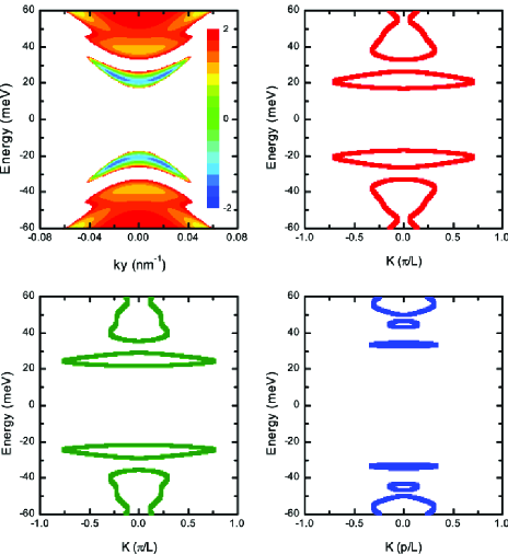
Let us consider a magnetic superlattice characterized by the barrier width , the inter-barrier distance , and the barrier height . In the magnetic superlattice, the alternating profile of magnetic barriers is taken into account as shown in Fig. 1(b). In this case, the period is given by . Figure 13 represents the contour plot of as a function of Fermi energy and , and exhibits band structures as functions of the Bloch wavevector . It is easily found that the band gap is consistent with the transporting gap shown in Fig. 5. Interestingly, there exist other forbidden gaps in the energy ranges [20:40] or [-40:-20]. Compared to the band gap between the conduction and valence bands, these gaps depend on values. (see Fig. 13(b)-(d)) Because of the -dependence, the conductance values are incompletely suppressed down, forming transmission dips around the energy ranges [20:40] as depicted in Fig. 5.
This formalism and the band structures are, of course, valid for only an infinite array of magnetic barriers. However, if the number of magnetic barriers are large enough, the qualitative analysis is expected to be quite consistent with the finite number of barriers.