Hopping conduction via ionic liquid induced silicon surface states
Abstract
In order to clarify the physics of the gating of solids by ionic liquids (ILs) we have gated lightly doped -Si, which is so well studied that it can be called the ”hydrogen atom of solid state physics” and can be used as a test bed for ionic liquids. We explore the case where the concentration of induced holes at the Si surface is below , hundreds of times smaller than record values. We find that in this case an excess negative ion binds a hole on the interface between the IL and Si becoming a surface acceptor. We study the surface conductance of holes hopping between such nearest neighbor acceptors. Analyzing the acceptor concentration dependence of this conductivity, we find that the localization length of a hole is in reasonable agreement with our direct variational calculation of its binding energy. The observed hopping conductivity resembles that of well studied implanted Si MOSFETs.
I Introduction
In the last decade room temperature ionic liquids revolutionized the way in which weakly conducting or insulating materials are gated in order to make them metallic or superconducting. By using an ionic liquid (IL) one can achieve surface carrier densities of within the electrochemical window of the electrolyte, which is of the order of a few volts.Petach et al. (2014); Ong et al. (2011)
Ionic liquids are molten salts made of negative and positive ions with relatively large radii. As a result, the Coulomb attraction energy of two adjacent opposite sign ions, , is small enough so that at room temperature the salt stays molten. Here nm is the sum of radii of positive and negative ions and is the dielectric constant of the IL. A negative voltage, applied between a metal coil submerged in the IL and the sample, causes negatively charged ions (anions) to migrate to the sample surface. At the sample surface an electric double layer is formed, which can be viewed as a capacitor with nm scale separation between electrodes. The crucial advantage of IL gating is that the IL-Si junction is insulating.
So far most of the research has dealt with gating of novel materials, such as rubrene Xie et al. (2014), underdoped YBCO Leng et al. (2012), polymers Wang et al. (2012), nanocrystal arrays Liu et al. (2010), nanotubes, and graphene Fujimoto and Awaga (2013), and has been aimed at the record induced carrier densities.
In this paper we focus on the basics of gating with ILs. For this purpose we choose to gate a lightly doped single crystal -type Si wafer. Silicon is so well studied that it can be called “the hydrogen atom of solid state physics” and, therefore, used as a “test bed” for ILs. At large surface densities the IL charge layer is usually regarded as an uniform sheet. In this paper we consider relatively small negative gate voltages, when the concentration of surface holes is in the range of . In this case each excess ion driven to the surface should be treated as a discrete charge individually responsible for creation of a carrier in a sample.
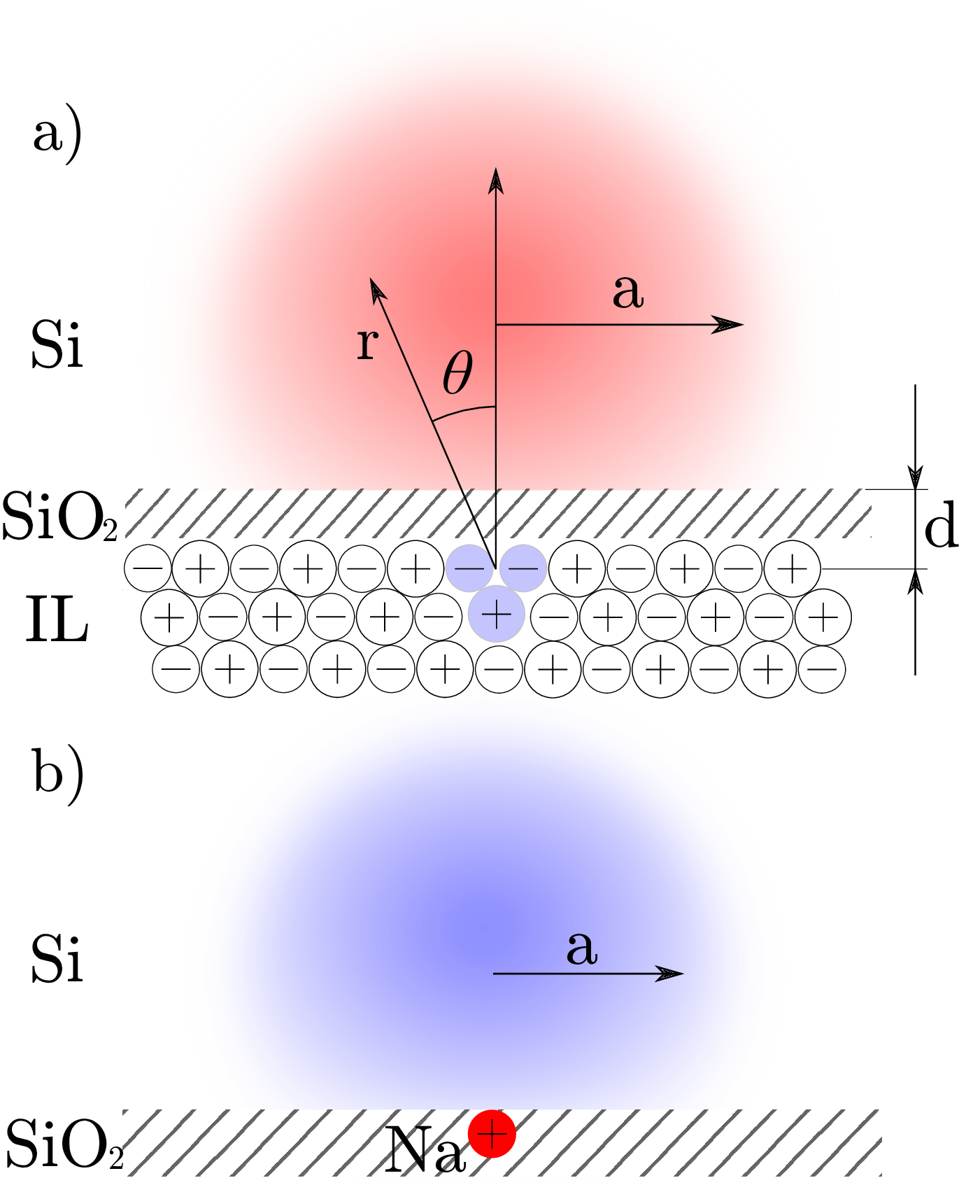
In the absence of an applied gate voltage, the IL is a neutral and strongly correlated liquid. When the arrangement of positive and negative ions resembles that of NaCl. When the gate is negatively biased, additional anions are driven to the sample surface. This results in discrete excess negative ions imposed on the neutral background with NaCl-like order. An example of such a net negative group of ions at the surface of Si is shown on Fig. 1a. Below we present evidence that suggests the excess anion binds a hole residing in Si (see the hole wave function cloud in Fig. 1a.) 111Previously the role of discrete excessive charges in IL was explored in the theory of double layer capacitance of IL-metal Loth et al. (2010). One can notice that such a IL surface acceptor is similar to the surface donor in Si MOSFETs as shown in Fig. 1b.Ando et al. (1982)
In the experiments, the ions were implanted on the top of layer of and driven by a positive gate voltage to the Si surface. Each ion binds an electron near the Si surface, becoming a surface donor. The surface conductivity as a function of temperature was shown to follow
| (1) |
where is the activation energy and the conductivity prefactor. Ando et al. (1982) The first term, which represents the activation of electrons to the conduction band with the activation energy equal to the ionization energy of the donor, dominates at high temperatures. The second term, observed at low temperatures, describes the nearest neighbor hopping between the donor states at the Si surface. (Some compensation of Na+ donors by acceptors creates empty donors and allows nearest neighbor hopping to proceed.)
In this work we show that IL gating of -type Si leads to a similar transport phenomenon. We observe the nearest neighbor hopping with the activation energy changing with the gate voltage, while the first term of Eq. (1) is shorted by the bulk conductance. This confirms the existence of discrete and sparse IL acceptors at the Si surface shown in Fig. 1a.
The remainder of this paper is organized as follows. In the following Section II we discuss our experimental set up. In Section III we present our experimental results and their analysis. In Section IV we discuss our model of IL gating of -Si with a Pt electrode and explain the origin of the negative threshold voltage. In Section V we theoretically evaluate parameters of the surface acceptor and compare them with our experimental results. We conclude in Section VI.
II Experimental Details
In our experiment we made ohmic contacts to a boron doped Si wafer after annealing it in a mixture of and in order to reduce the number of dangling bonds at the surface. A glass cylinder attached to the Si surface was used to confine the ionic liquid and control the gated area between contacts. The gate electrode consisted of a Pt metal coil suspended in the ionic liquid DEME-TFSI. The resistivity of the wafer is which with the typical hole mobility in Si of corresponds to a boron concentration of . This concentration is smaller than 3D concentration of () induced by the gate in the surface layer which has a width of (see below). Additional experimental details can be found in the Supplemental Material of Ref. Nelson and Goldman, 2015.
Other experiments have reported the possible role of electrochemical reactions when gating with an IL Jeong et al. (2013); Petach et al. (2014). To avoid these reactions we modulated the carrier density below room temperature at K, where the IL ions are still mobile. A thin oxide was used to protect Si from further oxidation and in addition, to passivate the trapping sites on the Si surface Gallagher et al. (2015); Cobbold (1970). This native oxide has a thickness of as measured by ellipsometry (a thicker oxide would reduce the capacitance of the transistor).
The 4-terminal sheet resistance of the silicon channel was measured by the van der Pauw method. In our previous study Nelson and Goldman (2015) we showed that the temperature dependence of the resistance at each gate voltage was reproducible during the cooling to 2 K and warming up to 230 K.
To calculate the surface concentration one can, in principal, use the capacitance of the device. However, in such a structure the total capacitance depends on both the geometrical and quantum capacitance Uesugi et al. (2013). The last one can be calculated for a degenerate gas with high hole concentration Uesugi et al. (2013) or for small concentrations Skinner and Shklovskii (2010). But our situation is one of intermediate concentration when the distance between holes is comparable with the Bohr radius of a hole. In this case one cannot use these formulas. Doing so would lead to uncertainties in the capacitance value. Therefore, to calculate the surface hole concentration we rely on integration of the charging current.
Just like in the experiments we do not observe the surface conduction until a certain sample dependent threshold gate voltage is reached 222The definition of threshold gate voltage is slightly different from the conventional one. At a gate voltages lower than an additional anion brings and binds a free hole from the bulk of the Si sample, becoming a shallow acceptor. Therefore, the two-dimensional hole density, , at was calculated by integrating the current during the charging process starting from . The dependence of the integrated carrier density on the applied gate voltage 333Our device is not equipped with a reference electrode to quantify the amount of applied gate voltage that actually drops across the interface between the IL and Si as it was done for example in Braga et al. (2012); Paulsen and Frisbie (2012). This is not an issue as was not used in the calculation of the sheet carrier density. is shown on Fig. 2. 444To study the low carrier density limit, we initially charged a sample to the conducting state and discharged it in small steps to study the low carrier density behavior. The data was taken until where surface state conduction vanishes. The voltage steps (100 meV) used in this experiment lead to current spikes of around 50 nA when was changed. Within 10 s of altering the current decayed back down to the noise floor of the system. While the charging process appears to only last for a few seconds the sample remained at a temperature where the IL was in a liquid state for several minutes. Waiting for longer than a few minutes had no effect on the surface state resistance.

From the slope of the dependence of on one can find the capacitance of the device . Assuming that dielectric constant of the IL and the is the same the related distance between negative ions in the IL and the holes in Si is . This agrees reasonably with the sum of the size of the ion and the width of the layer.
Since our device has a large area and we drive relatively large current the noise contribution to the accumulated charge is negligible.
III RESULTS
Plotted as a function of inverse temperature, the sheet resistance is shown in a logarithmic scale in Fig. 3 at different corresponding to four different concentrations of holes. Above , plotted in this way follows a straight line independent of
| (2) |
where and is a prefactor. The ionization energy of a Boron acceptor in Si is known to be , so that it is natural to assume that this line corresponds to the bulk conductance. Below , continues to follow activated temperature behavior, but with a dependent activation energy.
It is natural to interpret this low temperature part of Fig. 3 as the nearest neighbor hopping conductivity of holes between IL acceptors, which can be described by the second term of Eq. (1).
In our -type Si samples ; therefore, the part of the surface conductivity of Eq. (1) is shorted by the bulk conductance. This shorting does not occurs in doped samples because they are in the inversion layer regime, where the conducting path between source and drain electrode is insulated from the bulk of the sample by the hole depletion layer, while in our case we deal with an accumulation layer.
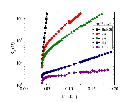
From each plot of Fig. 3 we extracted the prefactor and the activation energy which are shown in Fig. 4 and Fig. 5 respectively, as functions of the carrier density . For comparison we added the corresponding data for the nearest neighbor hopping conduction of implanted Si MOSFETs as summarized in Table III of Ref. Ando et al., 1982. Remarkably, the two experiments cover the same range of carrier concentrations and show similar hopping parameters.
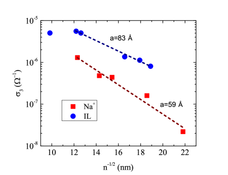
The dependence can be compared with the theoretical prediction based on the percolation approach Ambegaokar et al. (1971); Pollak (1972); Shklovskii and Efros (1971); Shklovskii (1972) as explained in Chapters 5 and 6 of Ref. Shklovskii and Efros, 1984. The two-dimensional analog of Eq. (6.1.9) with the help of Table 5.3 gives
| (3) |
where is a conductivity prefactor. In Fig. 4 we compare our data with Eq. 3. A reasonably good fit of the data is provided by the two straight lines corresponding to this equation. For the decay lengths we get for Na and for IL. The relatively large error in for the IL case comes from the accuracy of our carrier density which was determined from the uncertainty in to be .
IV Model of ionic liquid gating
Let us present our model of IL gating in greater detail than in the introduction. Let us discuss what happens when a Pt electrode gates -Si crystal with help of an IL but still at . The work function of Pt, , while the work function of -Si, , where is the electron affinity and is the band gap of Si. In equilibrium the electrochemical potentials of Pt and -Si have to be equal. This means that electrons are transfered from -Si to Pt. This results in a positively charged -Si and a negatively charged Pt. The resulting electric field between them is compensated by the IL polarization, so that anions move to -Si and cations move to the Pt surface. The voltage difference drops at the capacitance of the IL/Si surface, because the area of the Pt electrode is much larger than that of the Si one. Thus, there is an excess number of anions on the Si surface even in an equilibrium. This means that ideal contact Pt/IL/Si accumulates a layer of holes in Si. In such a situation, the Si wafer surface would be a good -type conductor.
In fact the situation is different. An ungated -type Si wafer is covered by a thin oxide layer. It is known that the oxide-silicon interface contains a substantial concentration of oxygen vacancies, which play the role of surface donors in -Si Deal et al. (1967). This results in an inversion layer of electrons on the ungated surface of -Si. In other words, the Si bands are bent downwards by the value of the Si gap creating a pocket for electrons while holes are depleted in a wide layer near the surface.
Let us see what happens when such a real surface is gated by an IL with a Pt electrode. In this case, -Si donates some of its electrons to Pt and becomes positive. As result of the IL polarization an equal number of anions move close to the Si surface forming a capacitor with positive donors. Actually at the temperature 230 K where gating is done the Coulomb attraction energy of an anion to a positive donor is substantially larger than so that most of the anions form compact pairs with empty positively charged donors. The remaining donors still create a downward bending of the conduction and valence bands and the depletion layer of holes, but this bending is smaller than and does not create an inversion layer near the surface. Thus, at the Si surface is an insulator.
To make it conducting we apply the negative . This threshold voltage brings enough anions to the Si surface to neutralize all the remaining donors. When all the donors are paired with anions, the electric field applied to Si and the downward bending of the Si the bands near the Si surface vanish, making the bands flat. At excessive anions bend the bands near the surface upwards and form a hole accumulation layer. Each excess anion binds a Si hole forming a surface acceptor discussed in the Introduction and shown in Fig. 1. These acceptors overlap weakly with each other. At the same time their effective three-dimensional density easily exceeds the density of the bulk B impurities so that at low temperatures the nearest neighbor hopping of holes between surface acceptors dominates the sample conductance (see Fig. 3).
Recall that surface acceptors are situated on a background of many compact pairs of donors and anions. These pairs are compact dipoles and create only a relatively weak random potential. In the following discussion of nearest hopping transport of holes on surface acceptors we ignore the potential of typical pairs. However, a small fraction of these pairs plays an important role in nearest neighbor hopping. These are pairs, which are thermally dissociated, i. e. where donors have their partner anion lost to the bulk of the IL. Such ionized donors play the role of a compensating impurity for the nearest neighbor hopping. They are responsible for the small number of empty surface acceptors, which allow holes to move along chains of surface acceptors (see Chapter 3 of Ref. 19).
V Binding energy and the hole decay length of the surface acceptor
In this section we theoretically calculate the binding energy and the decay length for an isolated IL acceptor shown in Fig. 1a. Let us first review the acceptor theory in the bulk -Si. It is known that the valence band is doubly degenerate and has two types of holes, light and heavy, with masses , respectively, here is the electron mass. It is known D’yakonov and Gelmont (1972) that for the above ratio the ground state energy of the acceptor is , where and is the dielectric constant of Si. If we assume that a bulk acceptor can be treated as a hydrogen atom with a hole mass , then the wave function of the first excited -state vanishes at the acceptor location and has a binding energy Pasquarello et al. (1989).
Let us now switch to the IL acceptor. If the distance between the acceptor nucleus and Si surface, , is so small that , one can assume, in the zero approximation, that the hole is also located just near the interface. Then the interaction between the hole and acceptor can be described by an effective dielectric constant , where is the dielectric constant of . (For simplicity we make the approximation that dielectric constant of the IL is that of .) The interface between and Si is treated as an infinite barrier, so that the wave function of the hole vanishes at the interface. The ground state for a hole in the half space is the first excited state for a hole in bulk with a corrected dielectric constant , i.e. , where . At the same time, the decay length is determined by the light mass
| (4) |
For we get .
Above we did not take into account that a hole interacts with its image charge and that is not zero. To do so, we use a variational approach with a probe hole wave function
| (5) |
Here we use spherical coordinates shown in Fig. 1a, is the distance between the acceptor and the hole, is the polar angle and the distance minimizes the energy:
| (6) |
Here the integration is over the Si half space, ranges from 0 to and ranges from to The Hamiltonian for the problem is
Here the first term represents the kinetic energy of a hole in Si. The second term is the potential energy of interaction of the hole with the acceptor . The third term is the interaction between the hole and its image in . As a rough estimate, we choose as the sum of the width of layer, and the radius of the negative ions in the IL (TFSI) to be . In the result, for we get that and . This decay length for a single acceptor can be considered as a reasonable estimate from below to the experimental . The concentrations of carriers which we work with are far from the case of the light doping when the separation between acceptors is much larger than . The wave function overlap of neighboring acceptors leads to an additional increase of the experimental value of .
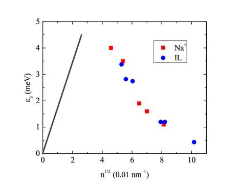
The fact that the overlap between acceptor states is substantial is also supported by Fig. 5. Here the straight line follows the equation:
| (8) |
which we derived for a two-dimensional lightly doped and weakly compensated semiconductor in a manner similar to the derivation for three-dimensional case in Ref. Efros et al., 1972 (see also Chapter 3 in Ref. Shklovskii and Efros, 1984). Equation (8) takes into account only classical shifts of levels of holes induced by the Coulomb potential of rare free of IL anions surface donors (see end of previous section IV) and ignores the overlap of hole wave functions. We see in Fig. 5 that in contrast to Eq. 8 the experimental values decrease with the growing . This happens because our concentrations are too large . At even larger concentrations the activation energy vanishes and the system goes through the metal-insulator transition studied in the Ref. Nelson and Goldman, 2015. In three-dimensional semiconductors a larger range of concentrations was studied, which displayed both regimes of growing and decreasing (see Fig. 8.1 in Ref. Shklovskii and Efros, 1984).
The ground state energy of Na+ donors near the surface of Si was estimated in Ref. Ando et al., 1982. This case is complicated by an additional electric field in the inversion layer which tends to localize electrons near the interface , to increase the donor ionization energy and to decrease the decay length of the wave function of a single donor. For experimental values of the electric field, the energy meV was obtained in Ref. Martin and Wallis, 1978; Ando et al., 1982. Using Eq. (4) and electron light mass we arrive at . Again, due to the high experimental concentration , this value can be considered to be a reasonable estimate from below for the experimental result .
VI Conclusion
We have explored the surface conductivity of Si gated by an ionic liquid. We studied small induced concentrations of holes below and showed that at such concentrations the transport is due to the nearest neighbor hopping between acceptor like states formed by sparse excessive negative ions of the IL. This transport is similar to the nearest neighbor hopping between Na+ donors in Na+ implanted Si MOSFETs. The similarity is not only qualitative but also quantitative due to the similar average masses of holes and electrons in Si. This brings us to the conclusion that an ionic liquid acts as a set of sparse acceptors on the surface of Si.
In the future it would be interesting to extend these results to smaller hole densities, where our theory should work better. One can study different ILs and see how the sizes of ions and dielectric constant of ILs affect hopping conductivity. One can also extend this work to new challenging materials using the same IL so that contrasting results with Si will help to understand better the parameters of these materials. For example, the extension of measurements of surface conductivity in IL gated rubrene Xie et al. (2014) to lower hole concentrations may help to understand nature and parameters of charge carriers.
Acknowledgements.
We are grateful to H. Fu for careful reading of the manuscript and C. Leighton and B. Skinner for helpful discussion. J. N. and A. M. G. were supported by the National Science Foundation (NSF) under award DMR-1263316. K. V. R. and B. I. S. were supported primarily by the National Science Foundation through the University of Minnesota MRSEC under Award Number DMR-1420013. Devices were fabricated at the Minnesota Nanofabrication Center which receives partial support from the NSF through the NNIN program.References
- Petach et al. (2014) T. A. Petach, M. Lee, R. C. Davis, A. Mehta, and D. Goldhaber-Gordon, Phys. Rev. B 90, 081108 (2014).
- Ong et al. (2011) S. P. Ong, O. Andreussi, Y. Wu, N. Marzari, and G. Ceder, Chemistry of Materials 23, 2979 (2011).
- Xie et al. (2014) W. Xie, S. Wang, X. Zhang, C. Leighton, and C. D. Frisbie, Phys. Rev. Lett. 113, 246602 (2014).
- Leng et al. (2012) X. Leng, J. Garcia-Barriocanal, B. Yang, Y. Lee, J. Kinney, and A. M. Goldman, Phys. Rev. Lett. 108, 067004 (2012).
- Wang et al. (2012) S. Wang, M. Ha, M. Manno, C. D. Frisbie, and C. Leighton, Nat Comms 3, 1210 (2012).
- Liu et al. (2010) H. Liu, A. Pourret, and P. Guyot-Sionnest, ACS Nano 4, 5211 (2010).
- Fujimoto and Awaga (2013) T. Fujimoto and K. Awaga, Phys. Chem. Chem. Phys. 15, 8983 (2013).
- Note (1) Previously the role of discrete excessive charges in IL was explored in the theory of double layer capacitance of IL-metal Loth et al. (2010).
- Ando et al. (1982) T. Ando, A. B. Fowler, and F. Stern, Rev. Mod. Phys. 54, 437 (1982).
- Nelson and Goldman (2015) J. Nelson and A. M. Goldman, Phys. Rev. B 91, 241304 (2015).
- Jeong et al. (2013) J. Jeong, N. Aetukuri, T. Graf, T. D. Schladt, M. G. Samant, and S. S. P. Parkin, Science 339, 1402 (2013).
- Gallagher et al. (2015) P. Gallagher, M. Lee, T. A. Petach, S. W. Stanwyck, J. R. Williams, K. Watanabe, T. Taniguchi, and D. Goldhaber-Gordon, Nat Commun 6, 6437 (2015).
- Cobbold (1970) R. Cobbold, Theory and applications of field-effect transistors (Wiley-Interscience, 1970).
- Uesugi et al. (2013) E. Uesugi, H. Goto, R. Eguchi, A. Fujiwara, and Y. Kubozono, Scientific Reports 3, 1595 (2013).
- Skinner and Shklovskii (2010) B. Skinner and B. I. Shklovskii, Phys. Rev. B 82, 155111 (2010).
- Note (2) The definition of threshold gate voltage is slightly different from the conventional one.
- Note (3) Our device is not equipped with a reference electrode to quantify the amount of applied gate voltage that actually drops across the interface between the IL and Si as it was done for example in Braga et al. (2012); Paulsen and Frisbie (2012). This is not an issue as was not used in the calculation of the sheet carrier density.
- Note (4) To study the low carrier density limit, we initially charged a sample to the conducting state and discharged it in small steps to study the low carrier density behavior. The data was taken until where surface state conduction vanishes. The voltage steps (100 meV) used in this experiment lead to current spikes of around 50 nA when was changed. Within 10 s of altering the current decayed back down to the noise floor of the system. While the charging process appears to only last for a few seconds the sample remained at a temperature where the IL was in a liquid state for several minutes. Waiting for longer than a few minutes had no effect on the surface state resistance.
- Ambegaokar et al. (1971) V. Ambegaokar, B. I. Halperin, and J. S. Langer, Phys. Rev. B 4, 2612 (1971).
- Pollak (1972) M. Pollak, Journal of Non-Crystalline Solids 8-10, 486 (1972).
- Shklovskii and Efros (1971) B. Shklovskii and A. Efros, Sov. Phys.- JETP 33, 468 (1971).
- Shklovskii (1972) B. Shklovskii, Sov. Phys.- JETP 34, 1084 (1972).
- Shklovskii and Efros (1984) B. I. Shklovskii and A. L. Efros, Electronic properties of doped semiconductors (Springer, 1984).
- Deal et al. (1967) B. E. Deal, M. Sklar, A. S. Grove, and E. H. Snow, Journal of The Electrochemical Society 114, 266 (1967).
- D’yakonov and Gelmont (1972) M. I. D’yakonov and B. L. Gelmont, Sov. Phys. Semicond. 5, 1905 (1972).
- Pasquarello et al. (1989) A. Pasquarello, L. C. Andreani, and R. Buczko, Phys. Rev. B 40, 5602 (1989).
- Efros et al. (1972) A. L. Efros, B. I. Shklovskii, and I. Y. Yanchev, physica status solidi (b) 50, 45 (1972).
- Martin and Wallis (1978) B. G. Martin and R. F. Wallis, Phys. Rev. B 18, 5644 (1978).
- Loth et al. (2010) M. S. Loth, B. Skinner, and B. I. Shklovskii, Phys. Rev. E 82, 056102 (2010).
- Braga et al. (2012) D. Braga, I. Gutirrez Lezama, H. Berger, and A. F. Morpurgo, Nano Letters 12, 5218 (2012).
- Paulsen and Frisbie (2012) B. D. Paulsen and C. D. Frisbie, The Journal of Physical Chemistry C 116, 3132 (2012).