Surface polarization and edge charges
Abstract
The term “surface polarization” is introduced to describe the in-plane polarization existing at the surface of an insulating crystal when the in-plane surface inversion symmetry is broken. Here, the surface polarization is formulated in terms of a Berry phase, with the hybrid Wannier representation providing a natural basis for study of this effect. Tight binding models are used to demonstrate how the surface polarization reveals itself via the accumulation of charges at the corners/edges for a two dimensional rectangular lattice and for GaAs.
pacs:
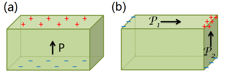
77.22.Ej, 73.20.-r, 71.15.-mFor over two decades, it has been understood that the electric polarization of an insulating crystal is a bulk quantity whose electronic contribution is determined modulo / (where is a lattice vector and is the unit cell volume) by the Bloch functions through a Berry-phase expression, or alternatively, in real space through the charge centers of the Wannier functions King-Smith and Vanderbilt (1993); Resta (1994). It was also shown that the macroscopic surface charge of an insulating crystal is predicted by the standard bound-charge expression (where is the surface normal) Vanderbilt and King-Smith (1993), as illustrated schematically in Fig. 1(a).
Here, we introduce and analyze a related quantity, the “surface polarization,” defined as a 2-vector lying in the plane of an insulating surface of an insulating crystal. By analogy with the bulk 3-vector , it has the property that when two facets meet, the linear bound-charge density appearing on the shared edge is predicted to be
| (1) |
where is the surface polarization on facet and is a unit vector lying in the plane of the facet and pointing toward (and normal to) the edge, as illustrated in Fig. 1(b).
This surface polarization is quite distinct from the dipole per unit area normal to the surface, which has also been called “surface polarization” by other authors Bányai et al. (1992); Wen et al. (2003). The latter is always present regardless of the symmetry of the surface, and manifests itself macroscopically through the surface work function. In contrast, our surface polarization lies in-plane and is nonzero only when the symmetry of the terminating surface supports a nonzero in-plane vector, as for example on the (110) surface of GaAs. It can also arise from a spontaneous symmetry-lowering surface reconstruction, as observed recently at the Pb1-xSnxSe (110) surface Okada et al. (2013) and predicted for an ultrathin film of SrCrO3 on SrTiO3 substrate (001) Gupta et al. (2013). The surface polarization will be most evident when the bulk vanishes, as will be the case for the systems discussed below.
The purpose of this Letter is to extend the Berry-phase theory to the case of surface polarization as defined above. To do this, we introduce a formulation based on hybrid Wannier functions (HWFs), which are Bloch-like parallel to the surface and Wannier-like in the surface-normal direction Sgiarovello et al. (2001); Wu et al. (2006); Soluyanov and Vanderbilt (2011); Taherinejad et al. (2014). This allows for the use of Berry-phase methods parallel to the surface while allowing a real-space identification of the surface-specific contribution in the normal direction. We illustrate the concept first for a “toy” 2D tightbinding (TB) model, demonstrating the method of calculating the surface polarization. We then consider an atomistic 3D model of an ideal (110) surface of a generic III-V zincblende semiconductor, using a TB model of GaAs to describe the electronic structure. In both cases, we confirm that the surface polarization correctly predicts corner and edge charges.
We first show how to express the surface polarization in terms of the Berry phases of HWFs for a 2D insulating sample, which we take to lie in the plane. We take the “surface” (here really an edge) to be normal to and introduce HWFs , where indexes unit-cell layers normal to the direction and runs over occupied Wannier functions in a single unit cell. For the bulk, the lattice is periodic in as well as , and the and their centers can be obtained using the 1D construction procedure given in Ref. Marzari and Vanderbilt (1997). To study the surface behavior we consider a ribbon consisting of a finite number of unit cells along . We then construct and diagonalize the matrix , whose eigenvectors yield the HWFs and whose eigenvalues give the HWF centers . In practice these are easily identified with the bulk covering the range of values that define the ribbon, with only modest shifts induced by the presence of the surface, allowing a common labeling scheme for both.
If we were interested in computing the dipole moment normal to the surface, we could obtain this from an analysis of the -averaged positions of the HWFs, where is the lattice constant along . However, our purpose here is different: we want to compute the polarization parallel to the surface. For this, we compute the Berry phase
| (2) |
of each HWF “band” as runs across the 1D BZ. Doing the same for the bulk HWFs (these are independent of ) and taking the difference, we obtain a set of Berry-phase shifts from which the electronic surface polarization can be determined via
| (3) |
where a factor of two has been included for spin degeneracy and is the edge repeat length in 2D. Since decays exponentially into the bulk, the sum will converge within a few layers of the surface, but for definiteness we sum to the center of the ribbon. If the values of some neighboring HWF bands overlap, the procedure needs to be generalized by grouping the HWFs into layers and using a multiband generalization to assign contributions to each layer.
The generalization to a 3D crystal with surface normal to is straightforward. The HWFs are with centers . The surface polarization is then obtained by computing Berry phases with respect to as before, averaging over all , and multiplying by the lattice constant divided by the surface cell area . The other surface polarization is given by the same formalism but with and reversed.
In the models considered in this paper, the surface polarization is purely electronic, as the ions are held fixed in their bulk positions. More generally, with the ionic contribution given by , where and are the position and bare charge of ion in cell , and is the corresponding bulk position of the same atom.
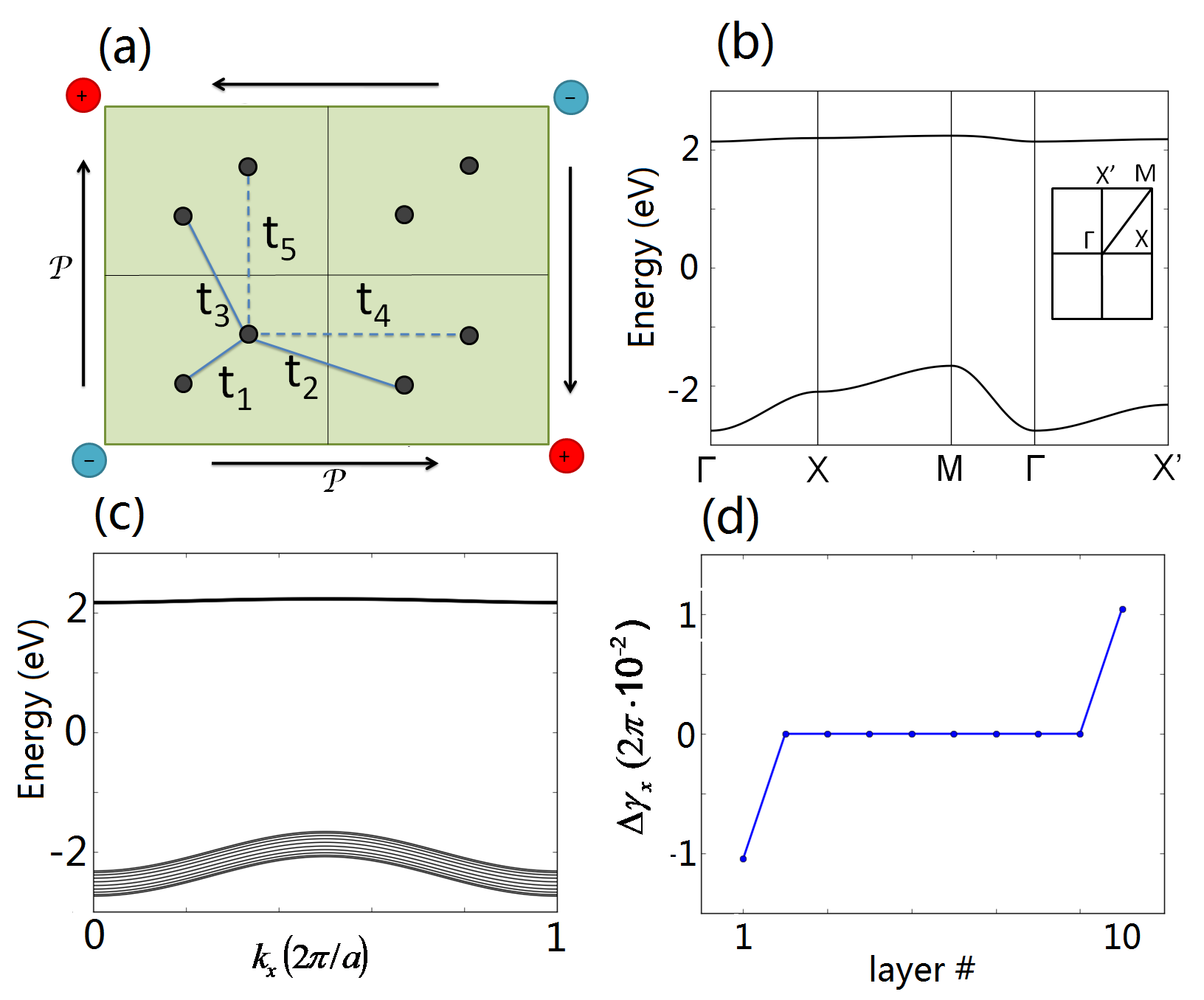
To illustrate these ideas, we start by considering a tight-binding (TB) model of the simple 2D crystal shown in Fig. 2(a). We assume a rectangular lattice with an aspect ratio . There are two atoms symmetrically located along a diagonal of the rectangular unit cell with coordinates () and (,), so that the bulk crystal has inversion symmetry. We consider only one orbital per atom with onsite energy taken to be zero, and assume that each atom contributes one electron so that only the lower band is (doubly) occupied. We take the nonzero hoppings to be those shown in Fig. 2(a) and choose their values to be , , and , and in eV. The position operators are taken to be diagonal in the local-orbital representation so that .
We plot the bulk band structure of the TB Hamiltonian in Fig. 2(b). For the selected parameters the band gap is large compared to the band widths; in particular, the upper (unoccupied) band is quite flat. Next we compute the surface polarization of a ribbon cut from the 2D lattice, taking it to be ten unit cells thick along and infinite along . For the atoms in the surface layers, the hoppings to the interior atoms are the same as those described above, while the hoppings to the vacuum side are set to zero. We used an equally spaced 60-point grid. At each the Hamiltonian is diagonalized, resulting in the band structure shown in Fig. 2(c). There are no obvious surface states, and in fact the result looks almost indistinguishable from a surface projection of the bulk band structure. The eigenfunctions are expressed in the tight-binding basis as , where the are the Bloch basis function formed as a Fourier sum at wavevector of atomic orbitals . From the ten occupied bands we construct the position matrix . Diagonalizing this matrix, we get ten eigenvalues that can each be clearly associated with a particular unit cell layer, and ten eigenfunctions that are the HWFs. We label the HWF , where is the layer index running from the bottom to the top of the ribbon.
Next we calculate , the Berry phase along , for each using Eq. (2). Deep in the interior these Berry phases become equal to within numerical precision, while the Berry phases near the edge are slightly shifted away from , leading to a nonzero surface polarization as shown in Fig. 2(d).
The value of the surface polarization obtained from Eq. (3) is for the top and bottom surfaces respectively. Similarly we can compute the surface polarizations for the left/right surfaces using a ribbon ten cells wide in and infinite along . We obtain along the left and right edges respectively. At the corners, the surface polarizations are directed head-to-head or tail-to-tail, as shown in Fig. 2(a).
Given the values of the surface polarizations in the 2D model, we predict that the charge accumulation at the corner of a finite sample should equal the sum of the two adjacent surface polarizations, here . To test this, we directly calculate the corner charge in a finite 2D sample, specifically a supercell, large enough to ensure neutrality in the central region and in the middle of the edges of the sample. The corner charge is obtained by summing up the on-site charge differences, relative to the bulk, for atoms in the quadrant containing the corner. We find for the top left and bottom right corners, and for the other two corners, in agreement with our prediction from the computed surface polarizations.
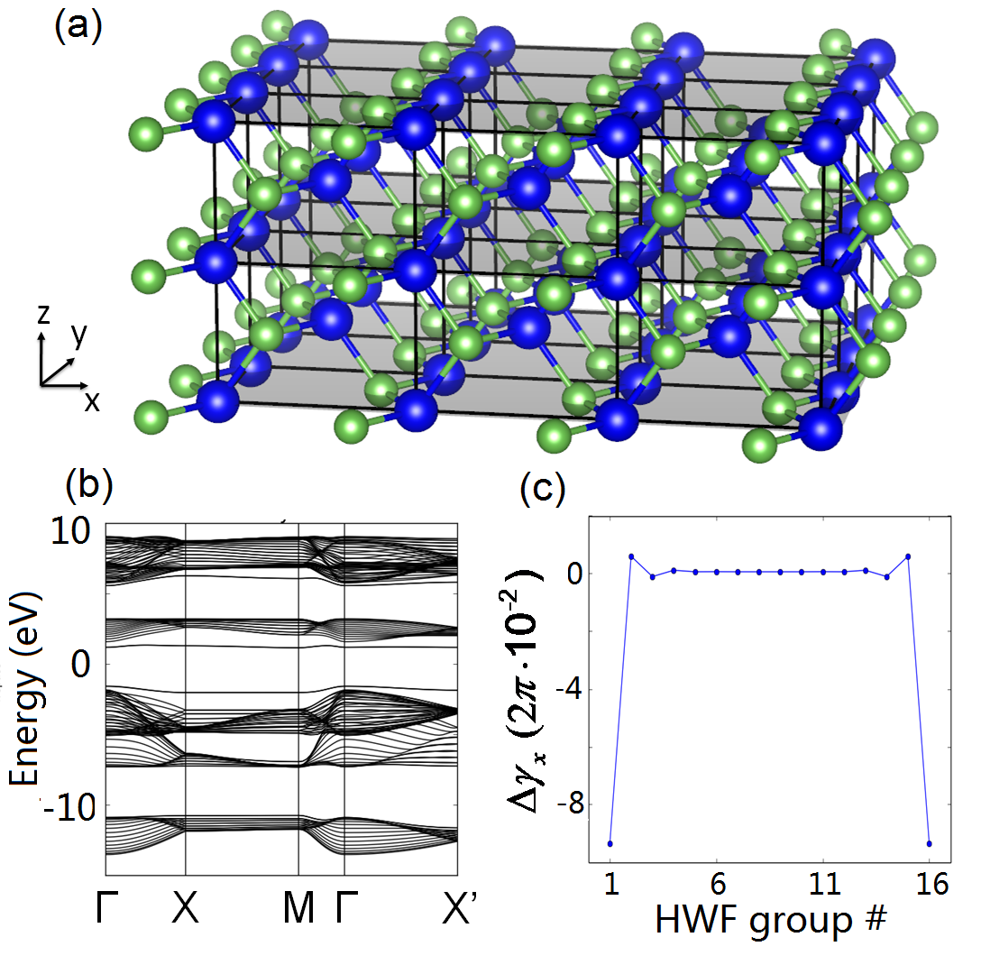
We now consider a TB model of a generic III-V zincblende semiconductor, with GaAs as the prototypical example. The crystal structure is characterized by Ga-As zigzag chains running along . Although the crystal structure does not have inversion symmetry, the tetrahedral symmetry forbids a nonzero spontaneous polarization. We use tight-binding parameters from Ref. Joannopoulos and Cohen (1974), in which is shown the bulk bandstructure and density of states. The unit cell contains two Ga and two As atoms, each with four hybridized orbitals and four electrons, as shown in Fig. 3(a). The position matrix is assumed to be diagonal and atom-centered in the basis of tight-binding orbitals.Bennetto and Vanderbilt (1996)
To describe the (110) surface, we construct a slab geometry as shown in Fig. 3(a), and we henceforth label the Cartesian directions as shown there. That is, the surface, which is normal to , has zigzag chains running along . Since the two atoms making up these chains are inequivalent, we expect a surface polarization in the direction. We take the slab to be eight unit cells thick; for the atoms in the surface layer, the hoppings to the atoms inside the slab are the same as in the bulk, while the hoppings to the vacuum side are set to zero. At each (,) of the grid in the surface BZ, the Hamiltonian is diagonalized, and we obtain the band structure for the slab, shown in Fig. 3(b). Surface states are evident as isolated bands.
Next, we diagonalize the 6464 position matrices constructed from the eigenstates of the occupied bands. The eigenvalues, which are the coordinates of the HWF centers, can be clearly divided into groups, each consisting of four HWFs representing the four Ga-As bonds around an As atom, each group being associated with one of the 16 atomic layers . In this case, it is more useful to calculate the Berry phase of each group of HWFs rather than of each single HWF Vanderbilt and King-Smith (1993).
As expected, the Berry phase in the direction along the zigzag chain is found to be zero, but in the direction it is nonzero for the HWF groups near the top and bottom surfaces of the slab. Thus, we confirm that there is a nonzero surface polarization . We plot the difference between the Berry phase of each group of HWFs and that for the bulk in Fig. 3(c). By summing up the contributions from each group of HWFs from the center of the bulk to one surface, the total surface polarization is found to be 0.178 . Here is the repeat length of the zigzag chain, i.e., the surface cell dimension along , where is the surface lattice constant along . Subdividing the dominant surface-group contribution further, we find that the surface polarization comes mainly from the surface-most HWF, corresponding to a shift of the center of the dangling bond on the surface As atom.
The surface polarization on the {110} surfaces predicts an accumulated line charge for the common edge of two such surfaces. In order to demonstrate this effect, we consider a hexagonal wire of GaAs that is infinite along [111], with a periodicity corresponding to three of the GaAs buckled (111) layers. In this case, the six side surfaces of the wire are all {110} planes: (), (), (), (), (), and (). As shown in Fig. 4(a), on each side facet the surface polarization is perpendicular to the zigzag chains, forming a pattern of vectors shown as black arrows. The surface polarizations for each neighboring pair of side facets have a common component along [111], but are head-to-head or tail-to-tail for the component normal to [111], leading to alternating positive and negative line charges for the six edges as shown. According to Eq. (1), we expect the line charge per three-layer vertical period to be , where the factor is the vertical period.
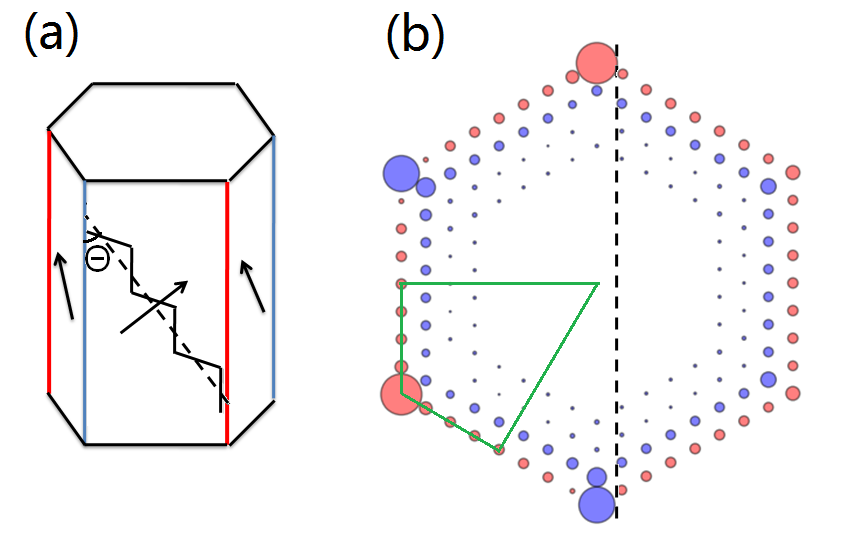
For comparison, we directly calculate the edge charges per trilayer period in a nanowire with a radius of 8 atoms. We sum up the site populations within the TB model with a 60-point grid along [111]. The onsite charge is the difference from the bulk value. The computed onsite charges are shown in the left half of Fig. 4(b), while the right half shows the corresponding results after averaging with a 60∘-rotated version of itself. The surface charges decay rapidly into the bulk, leading to a neutral bulk state inside the nanowire. Also, a surface dipole density normal to the surface is clearly visible, especially in the orientationally averaged results. However, we are interested in the accumulation at the edges, which is obviously present in the unaveraged results in the left half of the figure. The edge charge is calculated by summing up the onsite charges in the wedge-shaped region illustrated in Fig. 4(b), using a weight of 1/2 for atoms located on its radial edges. The total edge charge per trilayer is found to be 0.71, in agreement with the value predicted using the previously calculated surface polarization.
We emphasize that this numerical value is not intended to be realistic for GaAs. A more accurate estimate would require the use of an improved tight-binding model and treatment of surface relaxations and dielectric screening effects, or better, direct first-principles calculations. Our purpose here has been to show that the surface polarization as defined here correctly predicts edge charges. We note that an analysis based on maximally localized Wannier functions Marzari et al. (2012) is also possible. However, we believe our HWF-based approach is more natural, as the Wannier transformation is only done in the needed direction and no iterative construction is required.
We stress that the concept of surface polarization is quite general, occurring whenever the surface symmetry is low enough. In some cases this can arise from a spontaneous symmetry-lowering surface relaxation or reconstruction, allowing “surface ferroelectricity” if it is switchable. In other cases, as for GaAs (110), the ideal surface space group already has low enough symmetry to allow a nonzero . This will occur quite generally for low-angle vicinal surfaces. The concept also applies to planar defects such as domain walls, stacking faults, and twin boundaries, and to heterointerfaces; if is present within this plane, it may induce a line charge where the plane intersects the surface. Such edge and line charges are potentially observable using electric force microscopy Valdrè (2006) , electron holography Wolf et al. (2011), or other experimental methods. Finally we note that the concept of surface polarization may become more subtle in the presence of orbital magnetization, which we have omitted from our considerations here.
In summary, we have formulated the concept of surface polarization, i.e., the dipole moment per unit area parallel to the surface, which can exist whenever the surface symmetry is low enough. Using TB models we have computed the surface polarizations for a 2D toy model and a generic III-V zincblende semiconductor, and shown that the predicted corner or edge charges are in good agreement with direct calculations. We point out that surface and interface polarizations can be responsible for observable effects, and perhaps even desirable functionality, in a broad range of insulating materials systems.
We acknowledge helpful discussions with Hongbin Zhang, Jianpeng Liu and Massimiliano Stengel. This work is supported by NSF DMR-14-08838 and ONR N00014-11-1-0665
References
- King-Smith and Vanderbilt (1993) R. D. King-Smith and D. Vanderbilt, Phys. Rev. B 47, 1651 (1993).
- Resta (1994) R. Resta, Rev. Mod. Phys. 66, 899 (1994).
- Vanderbilt and King-Smith (1993) D. Vanderbilt and R. D. King-Smith, Phys. Rev. B 48, 4442 (1993).
- Bányai et al. (1992) L. Bányai, P. Gilliot, Y. Z. Hu, and S. W. Koch, Phys. Rev. B 45, 14136 (1992).
- Wen et al. (2003) W. Wen, X. Huang, S. Yang, K. Lu, and P. Sheng, Nat. Mater. 2, 727 (2003).
- Okada et al. (2013) Y. Okada, M. Serbyn, H. Lin, D. Walkup, W. Zhou, C. Dhital, M. Neupane, S. Xu, Y. J. Wang, R. Sankar, F. Chou, A. Bansil, M. Z. Hasan, S. D. Wilson, L. Fu, and V. Madhavan, Science 341, 1496 (2013).
- Gupta et al. (2013) K. Gupta, P. Mahadevan, P. Mavropoulos, and M. Ležaić, Phys. Rev. Lett. 111, 077601 (2013).
- Sgiarovello et al. (2001) C. Sgiarovello, M. Peressi, and R. Resta, Phys. Rev. B 64, 115202 (2001).
- Wu et al. (2006) X. Wu, O. Diéguez, K. M. Rabe, and D. Vanderbilt, Phys. Rev. Lett. 97, 107602 (2006).
- Soluyanov and Vanderbilt (2011) A. A. Soluyanov and D. Vanderbilt, Phys. Rev. B 83, 235401 (2011).
- Taherinejad et al. (2014) M. Taherinejad, K. F. Garrity, and D. Vanderbilt, Phys. Rev. B 89, 115102 (2014).
- Marzari and Vanderbilt (1997) N. Marzari and D. Vanderbilt, Phys. Rev. B 56, 12847 (1997).
- Joannopoulos and Cohen (1974) J. D. Joannopoulos and M. L. Cohen, Phys. Rev. B 10, 5075 (1974).
- Bennetto and Vanderbilt (1996) J. Bennetto and D. Vanderbilt, Phys. Rev. B 53, 15417 (1996).
- Marzari et al. (2012) N. Marzari, A. A. Mostofi, J. R. Yates, I. Souza, and D. Vanderbilt, Rev. Mod. Phys. 84, 1419 (2012).
- Valdrè (2006) G. Valdrè, Imaging & Microscopy 8, 44 (2006).
- Wolf et al. (2011) D. Wolf, H. Lichte, G. Pozzi, P. Prete, and N. Lovergine, Applied Physics Letters 98, 264103 (2011).