Spectroscopic evidence for two-gap superconductivity in the quasi-one dimensional chalcogenide Nb2Pd0.81S5
Abstract
We present the first direct evidence for two-band superconductivity in the quasi-one dimensional chalcogenide Nb2Pd0.81S5. Soft point contact spectroscopic measurements reveal Andreev reflection in the differential conductance in the zero-resistance superconducting (SC) state below (=6.6 K). Multiple peaks in were clearly observed at 1.8 K and were successfully explained by the two-band Blonder-Tinkham-Klapwijk model with two gaps meV and meV. Their evolution in temperature and magnetic field is consistent with the conventional BCS theory. The SC gap to ratio for and is 1.7 and 3.7, which is similar to the weak coupling BCS prediction of 3.5. These results demonstrate that the newly discovered niobium chalcogenide is a two-gap superconductor in the weak coupling limit.
Materials with low-dimensional electronic structure have attracted interest because they provide a rich avenue to explore various novel phases arising from strong electron correlations gozar08 ; berezinskii72 ; kosterlitz73 ; dresselhaus14 . A spin (or charge) density wave is one such example that occurs due to geometry of the Fermi surface in momentum space that is conducive to the development of a Peierls instability which leads to a spatial modulation of the spins (or charges). Unconventional superconductivity with a triplet superconducting (SC) order parameter, or a chiral d-wave symmetry was also proposed due to strong repulsive electron-electron interactions gorkov85 ; chubukov12 . An inhomogeneous superconducting phase with a periodic modulation in SC amplitude, or Fulde-Ferrel-Larkin-Ovchinnikov state, may also be realized at low temperature and high magnetic fields in low-dimensional compounds fulde64 ; larkin65 .
The newly discovered chalcogenide superconductor Nb2PdxS5 (or Nb215) has attracted interest because of its quasi-one-dimensional (1D) electronic structure zhang13 ; niu13 ; singh13 ; zhou13 ; ning15 ; biswas15 . Spin susceptibility is estimated to be strongly enhanced at small wavevectors, indicating that Nb215 is in close proximity to a magnetically ordered state with long modulation wave-lengths. When compared to its relatively low SC transition temperature ( K), its upper critical field is very high ( T), exceeding the Pauli limiting field expected for weakly coupled superconductors ( T). The temperature dependence of the upper critical field perpendicular to the chain direction (b-axis) does not saturate at low temperatures, but linearly increases with decreasing temperature. When combined with the strong dependence on temperature of the anisotropy and multiple Fermi surfaces, the linear-in- dependence of of Nb215 is indicative of multiband superconductivity zhang13 . Recent muon spin relaxation and rotation measurements, however, claimed a single s-wave energy gap from the temperature dependence of the magnetic penetration depth, thus requiring a more definitive study on the nature of SC gap in order to understand the SC mechanism of this low-dimensional superconductor.
Here, we report the first, direct evidence for two superconducting gaps in the chalcogenide superconductor Nb2PdxS5 (). Differential conductance , which is obtained via soft point-contact spectroscopy, shows an enhancement at zero-bias voltage below due to the Andreev reflection and multiple peaks become more distinguishable with decreasing temperature. A single band BTK (Blonder-Tinkham-Klapwijk) model fails to explain the spectroscopic features deep inside the SC state, while the two band BTK model best explains the two peak structure with meV and meV at 1.8 K. The magnetic field suppresses both the large and the small SC gaps, where a least-squares-fit with the BCS model reasonably explains the field dependence of both of them with T for , which is consistent with the previous report zhang13 . Taken together, these results prove the existence of multiple superconducting gaps in the newly discovered quasi-1D chalcogenide compound Nb2PdxS5.
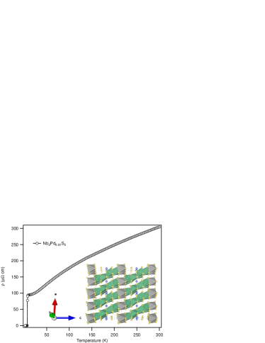
Single crystalline Nb2PdxS5 samples with were grown by solid reaction crystallizing in a monoclinic structure, where the Nb-S trigonal prisms are stacked along the b-axis forming conducting chain along that direction (see inset of Fig. 1) keszler85 ; khim13 . Electrical resistivity measurements were performed through the conventional four-probe technique on a needle like single crystal, where the electrical current is applied along the elongated b-axis. As shown in Fig. 1, the resistivity ratio between room temperature and , , is approximately 3, which is similar to the one previously reported zhang13 . The resistivity shows a sharp SC transition to a zero value at 6.6 K. In the following, we analyze the data below 6.6 K, where the zero-resistance state is established. In order to perform the soft point-contact spectroscopy (SPCS), silver grains from Dupont 4929N were applied on the surface of the sample gonnelli10 . Magnetic field is applied perpendicularly to the needle axis, i.e., axis. Tens of contacts, made on two different crystals from the same batch, showed consistent spectroscopic signatures with respect to one another, thus ensuring reproducibility of the differential conductance data reported in this Letter.
Figure 2(a) shows a representative plot of current as a function of the bias voltage (on the right ordinate) at 1.8 K (solid line) and 9 K (dashed line). The nearly linear characteristics for as well as the absence of dips in the differential conductance indicate that the effective contact size is close to the Sharvin limit PCSBOOK ; gonnelli10 . Here is the size of the SC gap. The dependence of on the bias voltage of at 1.8 K is shown on the left ordinate of Fig. 2(a) (open circles). Multiple peaks in , which are almost symmetric with respect to the zero-bias voltage, indicates two SC energy gaps for the Nb215 compound. As shown in Fig. 2(b), the second derivative of the differential conductance spectra, , reveals pronounced dips that correspond to the multiple peaks in . Even though data are scattered, the first derivative of the curve at 1.8 K is consistent with the obtained from an ac modulation technique (see Fig. S1, Supplementary Information), indicating that the multiple peak structure in represents intrinsic SC properties of the Nb215 superconductor.
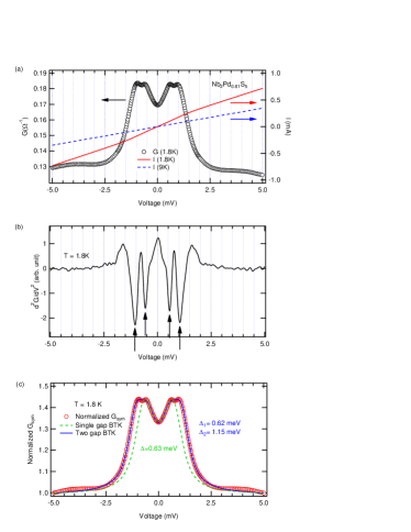
In order to quantitatively understand the multiple SC gaps for Nb215, the multi-gap BTK model is used and the total conductance is the sum of the multigap components with a weighting factor for the th component, or . The tunneling transparency of the point contact barrier and quasi-particle lifetime broadening effect were parametrized in the BTK model for the conductance between normal and superconducting phases gonnelli10 ; btk82 ; plecenik94 :
| (1) |
Here, is the Fermi-Dirac distribution function at a finite temperature and is the prefactor that depends on the density of states of the metallic tip and the SC material. The BTK integral kernel, , is written as
| (2) |
The transparency of the barrier is given by and the complex function , where and :
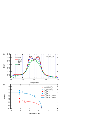
Figure 2(c) shows the normalized differential conductance at 1.8 K, where at positive voltage and at negative voltage is symmetrized and divided by the value at +5 mV, i.e., . A single band BTK model (dashed line) could explain the dip at zero bias voltage, but fails to explain the second dip at around mV. In contrast the two band BTK model (solid line) captures the characteristic features with meV, meV and the weight of the first gap . The amplitude of the two SC gaps is close to the value of the dip positions in the second derivative of the differential conductance dd, as shown in Fig. 2b. We note that a small value of less than 0.01 equally fits well the normalized conductance , indicating both a clean interface and a quasiparticle lifetime that is close to infinite at low temperatures. The least-squares fit based on the two-band BTK model best describes the data with effective tunneling barriers of 0.3 and 0.5 for the small and large SC gaps, respectively.
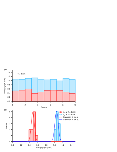
Figure 3(a) selectively shows the differential conductance of Nb215 for several temperatures in its SC state. The conductance dip at the zero-bias voltage, which is typical for Andreev reflection when , becomes shallower with increasing temperature and disappears completely for temperatures above 2.9 K due to thermal smearing effects. Another dip structure at mV for 1.8 K, which reflects the two-gap nature of the dichalcogenide superconductor, is also smeared out with increasing temperature due to thermal effects. The decrease in the dip position with increasing temperature is consistent with the decrease in the gap amplitude. The temperature dependence of the two SC gaps is shown in Fig. 3(b), where the gap amplitudes are obtained from the two-band BTK fitting (solid symbols) and from the dip in the second derivative of the differential conductance (open symbols) for several different contacts made on the ac-plane of different crystals. Solid lines depict the dependence expected from the weak coupling BCS theory, which reasonably describes the temperature dependence of the gaps with meV and meV.
Figure 4 shows statistical counts for ten different point contacts and the distribution of SC energy gaps obtained at 1.8 K from the second derivative of the differential conductance, dd, for Nb215. The small SC gap is concentrated between 0.4 and 0.6 meV, while the large SC gap is between 1.0 and 1.15 meV. As shown in Fig. 4(b), the statistical distribution can be explained by a Gaussian function, where the peaks are located at 0.48 0.02 and 1.05 0.04 meV for and , respectively. The SC gap ratios against , 2/kB, are 1.7 and 3.7, where the gap ratio for the large gap is close to the BCS prediction of 3.5 for weak coupling superconductors inosov11 . Recently, the temperature dependence of the specific heat for Nb2PdS5 was analyzed in terms of multiple SC gaps, where the small and large gap ratio is 1.9 and 6.4, respectively goyal15 . The difference between this work and Ref goyal15 may arise from the limited temperature range over which the specific heat was studied, i.e., K K. When measured down to 0.5 K, a similar specific heat study for another chalcogenide Nb2Pd1.2Se5 showed that the gap ratios are 2.1 and 4.1, which is similar to this work khim13 . We note that the gap values obtained from the two-band BTK model are consistent with those from dd.
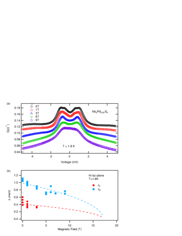
The dependence of the differential conductance of Nb215 at 1.8 K on the magnetic field is shown in Fig. 5(a), where is applied perpendicularly to the crystallographic -axis. For clarity, the conductance for each field is vertically displaced with respect to the zero-field spectrum. The multiple peaks observed at zero field are rapidly suppressed with increasing field, which could be due to a fast decrease in the Andreev reflection from the small SC gap under magnetic field. The dip observed at zero-bias voltage, which appears in the Andreev reflection for a finite , becomes blurred with increasing magnetic field. The pair-breaking effects induced by the magnetic field are indicated by the enhancement in the effective broadening parameter due to a reduction in the quasiparticle lifetime gonnelli10 ; naidyuk96 .
The magnetic field dependence of the SC energy gaps as determined from the dip positions in dd is shown in Fig. 5(b). The dashed lines are least-square-fits of the SC gaps for type-II superconductors, where the SC gap ratio is assumed to be independent of magnetic field morenzoni14 ; gross86 :
| (3) |
where and . The upper critical field at 1.8 K is 17 T, which is consistent with magneto-resistance measurements zhang13 .
To conclude, we have directly shown that the quasi-1D chalcogenide Nb2Pd0.81S5 is a two-gap superconductor, where the amplitude is 1.05 and 0.48 meV for the large and the small SC gaps, respectively. The differential conductance curves measured from soft point-contact spectroscopy for Nb215 were successfully explained by the two-band BTK model with a finite point contact barrier and a quasiparticle lifetime broadening effect . With increasing temperature, the multiple peak structure and the dip at the zero-bias voltage in the differential conductance become weaker due to thermal broadening. The temperature dependence as well as the magnetic field dependence of the SC gaps are in agreement with the BCS theory. The gap/temperature ratio for the larger gap is 3.7, which is slightly larger than BCS value of 3.5 for weakly coupled superconductors. Although the isotropic BTK model was successfully applied to describe the differential conductance of the Nb215 superconductor, its quasi-1D Fermi surfaces have yet to be taken into account to make a better understanding of the point contact spectra.
Work at Sungkyunkwan University was supported by a NRF grant funded by the Ministry of Science, ICT and Future Planning (No. 2012R1A3A2048816). Work at Los Alamos was performed under the auspices of the US Department of Energy, Office of Science, Division of Materials Science. Work at Zhejiang University is supported by the National Natural Science Foundation of China (Grant No. 11374257) and the Fundamental Research Funds for the Central Universities. LB is supported by DOE-BES through award DE-SC0002613.
References
- (1) A. Gozar, G. Logvenov, L. Fitting Kourkoutis, A. T. Bollinger, L. A. Giannuzzi, D. A. Muller, and I. Bozovic, Nature 455, 782 (2008).
- (2) V. L. Berezinskii, Sov. Phys. JETP 34, 610–616 (1972).
- (3) J. M. Kosterlitz and D. J. Thouless, J. Phys. C 6, 1181–1203 (1973).
- (4) M. S. Dresselhaus, Mater. Res. Lett. 2, 1 (2014).
- (5) L. P. Gor’kov and D. Jerome, J. Phys. Lett. Paris 46, L643 (1985).
- (6) R. Nandkishore, L. S. Levitov and A. V. Chubukov, Nat. Phys. 8, 158 (2012).
- (7) P. Fulde and R. A. Ferrell, Phys. Rev. 135, A550 (1964).
- (8) A. I. Larkin and Y. N. Ovchinnikov, Ov. Phys. - JETP 20, 762 (1965).
- (9) Q. Zhang, G. Li, D. Rhodes, A. Kiswandhi, T. Besara, B. Zeng, J. Sun, T. Siegrist, M. D. Johannes, and L. Balicas, Sci. Rep. 3, 1446 (2013).
- (10) C. Q. Niu, J. H. Yang, Y. K. Li, Bin Chen, N. Zhou, J. Chen, L. L. Jiang, B. Chen, X. X. Yang, Chao Cao, Jianhui Dai, and Xiaofeng Xu, Phys. Rev. B 88, 104507 (2013).
- (11) D. J. Singh, Phys. Rev. B 88, 174508 (2013).
- (12) N. Zhou, Xiaofeng Xu, J. R. Wang, J. H. Yang, Y. K. Li, Y. Guo, W. Z. Yang, C. Q. Niu, Bin Chen, Chao Cao, and Jianhui Dai, Phys. Rev. B 90, 094520 (2014).
- (13) W. Ning, H. Yu, Y. Liu, Y. Han, N. Wang, J. Yang, H. Du, C. Zhang, Z. Mao, Y. Liu, M. Tian, and Y. Zhang, Nano Lett. 15 (2), 869-875 (2015).
- (14) P. K. Biswas, H. Luetkens, Xiaofeng Xu, J. H. Yang, C. Baines, A. Amato, and E. Morenzoni, Phys. Rev. B 91, 100504(R) (2015).
- (15) D. A. Keszler, J. A. Ibers, S. Maoyu and L. Jiaxi, J. Solid State Chem. 57, 68 (1985).
- (16) S. Khim et al., New Journanl of Physics 15, 123031 (2013).
- (17) D. Daghero and R. S. Gonnelli, Supercond. Sci. Technol. 23, 043001 (2010).
- (18) Yu. G. Naidyuk, and I. K. Yanson, Point-contact spectroscopy, Springer Series in SOLID-STATE SCIENCES 145 1 (2005).
- (19) G. E. Blonder, M. Tinkham and T. M. Klapwijk, Phys. Rev. B 25 4515 (1982).
- (20) A. Plecenik, M. Grajcar, S. Benacka, P. Seidel, and A. Pfuch, Phys. Rev. B 49, 10016 (1994).
- (21) D. S. Inosov, J. T. Park, A. Charnukha, Yuan Li, A. V. Boris, B. Keimer, and V. Hinkov, Phys. Rev. B 83, 214520 (2011).
- (22) R. Goyal, B. Tiwari, R. Jha, and V. P. S. Awana, J. Supercond. Nov. Magn. (to be published DOI 10.1007/s10948-015-2961-5).
- (23) Y. G. Naidyuk, R. Haussler and H. V. Lohneysen, Physica B 218, 122 (1996).
- (24) E. Morenzoni et al., J. Phys.: Confer. Seri. 551, 012027 (2014).
- (25) F. Gross et al., Z. Phys. B - Condensed Mattter 64, 175 (1986).