graphical abstract
![[Uncaptioned image]](/html/1505.03041/assets/x1.png)
Simple Method for Large-Scale Fabrication of Plasmonic Structures
Abstract
A novel method for single-step, lithography-free, and large-scale laser writing of nanoparticle-based plasmonic structures has been developed. Changing energy of femtosecond laser pulses and thickness of irradiated gold film it is possible to vary diameter of the gold nanoparticles, while the distance between them can be varied by laser scanning parameters. This method has an advantage over the most previously demonstrated methods in its simplicity and versatility, while the quality of the structures is good enough for many applications. In particular, resonant light absorbtion/scattering and surface-enhanced Raman scattering have been demonstrated on the fabricated nanostructures.
With the advent and rapid progress of fabrication technology in the past few decades, there has been growing interest in the field of plasmonics to explore novel phenomena by manipulating light at nanoscale Maier (2007); Luk’yanchuk et al. (2010). Examples of plasmonic devices requiring ordered nanoparticles are plasmonic filters Kravets et al. (2008); Liu et al. (2008), metasurfaces Yu and Capasso (2014), and waveguides Maier et al. (2003). The research area dealing with the interaction of molecules or molecular structures with plasmonic nanostructures is another rapidly growing field, due to potential analytical applications such as surface-enhanced Raman spectroscopy (SERS) and localized surface plasmon resonance spectroscopy Moskovits (1985); Lal et al. (2007); Anker et al. (2008). In addition, plasmonic nanostructures exhibit strong nonlinear optical response that yields enhanced THz emission and high-harmonics generation Kauranen and Zayats (2012); Lee et al. (2014); Minovich et al. (2015).
To date, the most popular and controllable approaches of plasmonic nanostructures fabrication are based on direct ion-beam milling or multistage e-beam and nanoimprint lithographes. However, lithography-free and single-step methods are more desirable for large-scale manufacturing. Among single-step techniques, chemical syntheses of monodisperse nanoparticles colloid is a promising method for high-throughput fabrication, however it requires additional technological steps to order the nanoparticles into functional nanostructure Junno et al. (1995); Kraus et al. (2007); Shi et al. (2013); Patra et al. (2014). An alternative cost-effective and versatile approach is to exploit self-assembly process via dewetting of heated thin supported film of a wide range of materials Bischof et al. (1996); Higgins and Jones (2000); Abbarchi et al. (2014). Laser radiation Bischof et al. (1996); Trice et al. (2007); Wu et al. (2011), ion-beam Lian et al. (2006) or heating on a hotplate Higgins and Jones (2000); Abbarchi et al. (2014) have been utilized as heat sources for launching the dewetting process.
Another way is to employ cost-effective laser technologies in order to controllably create nanoparticles via precise ablation of thin films, exploiting single nanoparticle transfer to a receiver substrate after single-shot femtosecond (fs) laser irradiation of a thin film Kuznetsov et al. (2009, 2011); Zywietz et al. (2014) or direct two-shots writing of plasmonic nanoantennas coupled with plasmonic lenses Ionin et al. (2015).
Despite many different approaches have been proposed to fabricate Au nanoparticles, the successful implementation of plasmonic devices still requires cost-effective and versatile method of controllable large-scale fabrication of ordered Au nanoparticles.
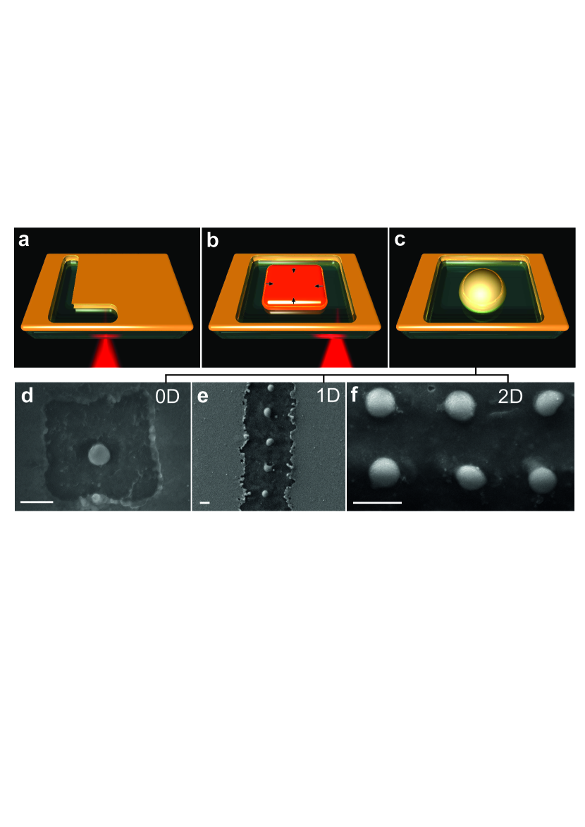
In this paper, we present a conceptually new, single-step, lithography-free and cost-efficient method for large-scale fabrication of nanoparticle-based plasmonic structures. The combination of simplicity of thin film dewetting process, along with precision and high-productivity of the laser technology enables extreme simplification of the process of nanoparticles fabrication, while the quality of fabricated structure is well-maintained. In other words, we achieve direct single-step “writing” of nanopartices by strongly focused femtosecond laser pulses, where the laser irradiation is used to pattern and heat-up the residual film to the dewetting temperatures. We implement this simple method for writing of 0D, 1D, and 2D plasmonic structures, and show their applicability for the optical and sensing problems.
First, strongly focused fs-laser beam irradiates a thin Au film at fluence slightly higher than the thin film ablation threshold, which increases in range of 15–70 mJ/cm2 with growth of the film thickness. These values are much lower than the values for single-shot ablation thresholds of thin gold films of corresponding thicknesses Kuznetsov et al. (2009); Ionin et al. (2015). Since the scanning conditions correspond to the number of pulses N104 and the time delay between the fs-laser pulses in train is 12.5 ns, temperature in the vicinity of irradiated area is gradually accumulated pulse-by-pulse and achieves the level of film ablation in a certain region. Importantly, there is almost no ablation debris nearby each groove, being a result of evaporative mechanism of ablation, rather than spallative one followed by random dissemination of sub-100 nm nanoparticles in the vicinity of heated area Zhigilei et al. (2009). In this regime, rather clean and narrow (width of 400 nm) grooves can be written directly on the surface (Fig. 1). It is worth noting that femtosecond pulse duration minimizes the heat affected zone Bauerle (2011), resulting in a shallow groove depth of about 30% deeper than the film thickness (see Supplementary Information).
Second, a single patch can be easily cut (Fig. 1b) with any size larger than the uncertainty of the grooves edges (50 nm, Fig. 1d,e). The cut patch is thermally isolated since the thermal conductivities of the silica substrate and air are two and four orders of magnitude smaller than gold, respectively. Therefore, the isolated patch can be easier heated up to the temperatures where the film undergoes dewetting process. The dewetting temperature of the films could be much lower than the melting point of bulk gold 1337 K. For instance, a 10-nm Au film on fused silica is dewetted even at 430 K, while 60-nm Au film undergoes dewetting at temperatures lower than 870 K Gadkari et al. (2005). Moreover, the smaller the patches (with smaller total volume), the higher the temperatures can be achieved at fixed fluence. As a result, the heated cut Au patch transforms into a nanoparticle of the same volume during the dewetting process (Fig. 1).
Although dewetting is a spontaneous process for homogeneous film Bischof et al. (1996); Trice et al. (2007), the reproducible formation of a certain number of nanoparticles has been demonstrated by heating of lithographicaly cut microscale patches of thin film Lian et al. (2006); Kim et al. (2009); Fowlkes et al. (2011); Wu et al. (2014); Abbarchi et al. (2014). Moreover, a single nanoparticle formation from each patch is possible, when patch width-to-height ratio (=w/h, where is the lateral size of the square patch and is the film thickness) is smaller than a certain value Kim et al. (2009). In the case of Au film on SiO2, this value must fulfill the condition 40, to provide almost 100 percentage probability of single particle formation with a certain diameter Kim et al. (2009). In our experiments we achieve the most controllable formation of nanoparticles at 15–30.
This technique enables direct writing of 0D (a single nanoparticle, Fig. 1d), 1D (a line of nanoparticles, Fig. 1e) and 2D (an array of nanoparticles, Fig. 1f) nanoparticle-based structures. The 2D structures are produced by laser beam scanning of the film surface in two orthogonal directions, allowing extremely high production rate 1 mm2/min at available speed of laser scanning 0.3 m/s. All types of the structures have been successfully fabricated on 20 and 30 nm Au films, while the other thicknesses (10 and 60 nm) provide much less controllable film patterning. Beside film thickness, another parameter that affects the diameter and quality of the nanoparticles is the width of the cut patch.
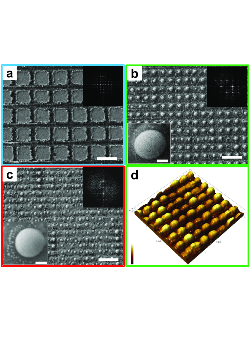
In Fig. 2, SEM images of the fabricated 2D structures 30-nm Au film are shown as a sequence of reduced period between -crossed laser scans at fluence of 40 mJ/cm2. The laser fluence is chosen to provide as narrow and reproducible as possible grooves. Evidently, there are four main regimes: (i) square micro-patches formation (Fig. 2a); (ii) unstable transition from square micro-patches to nanoparticles; (iii) formation of ordered and almost similar nanoparticles (Fig. 2b,d); (iv) formation of disordered different-size nanoparticles (Fig. 2c). The fabricated particles have almost spherical shape and are partly embedded into the substrate (Fig. 2d). Corresponding regimes are indicated in Fig. 3a, where one can see that size-dispersion of cut patches and nanoparticles is a non-monotonic function of the scans period. In particular, for =30 nm the size-dispersion demonstrates local minimum at scan period of 0.9–1 m, i.e. in the most stable and reproducible regime of ordered nanoparticles formation for 30-nm Au film.
For film thickness of =30 nm, we observe reproducible formation of sub-100 nm nanoparticles conglomerates nearby each ordered nanoparticle when periods of scan are smaller than 0.9 m (see inset of Fig. 2c). Similar behaviour has been observed when some parts of molten film are not absorbed by larger particles during dewetting process, and interpreted in terms of multimodal Rayleigh-Plateau instability Fowlkes et al. (2014). Indeed, the conglomerates are formed preferably from the side of last cutting of each patch (see left side in inset of Fig. 2c).
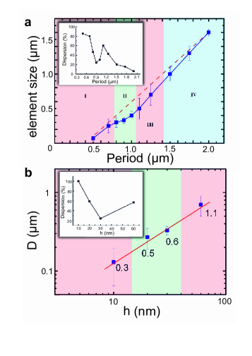
The experimental thickness dependence of the nanoparticles diameters exhibits almost linear (slope is 0.9) dependence over the whole range of Au films thicknesses (Fig. 3b), being a general trend for thin film dewetting Thompson (2012). As it was mentioned before, we observe a transformation of each patch into a single nanoparticle, which is due to the too small sizes of the patches Kim et al. (2009) in comparison with typical wavelength of Rayleigh-type instability driven by capillary waves Landau and Lifshitz (1987); Bischof et al. (1996). The value of wavelength of the dominating capillary wave on homogeneous film can be estimated as Wyart and Daillant (1990): , with the parameter being characteristic of the material combination substrate/film (4.3 nm for gold on fused silica Bischof et al. (1996)). Substituting our experimental parameters, we obtain the following estimations: (h=10 nm)0.12 m, (=20 nm)0.48 m, (=30 nm)1.1 m, and (=60 nm)4.3 m. Comparison of these values with corresponding values of plotted in Fig 3b shows that the optimal conditions for single nanoparticle formation can not be fulfilled only for =10 nm, which provides and comparable with the uncertainties ( 50 nm) of grooves edges.
Similar to the scan period (the patch width) dependencies, there are also some range of thicknesses where quality of the 2D nanoparticles array is the most optimal (Fig 3b). Non-monotonic behaviour of the size dispersion dependence on scan period and film thickness can be attributed to two main reasons: (i) the conditions 1 and 40 are not fulfilled for very small thicknesses and (ii) the dewetting temperature is much higher for thicker films. Therefore, too thin films can not provide ordered nanoparticles formation, while too thick and large patches can be hardly heated homogeneously during laser cutting to achieve controllable dewetting.
Gold nanoparticles are well known to provide resonant light absorption/scattering and local field enhancement in the optical range. In order to show high applicability of the proposed novel method, we examine basic optical properties of 2D nanoparticles arrays fabricated at different regimes: extinction and scattering spectra, and SERS.
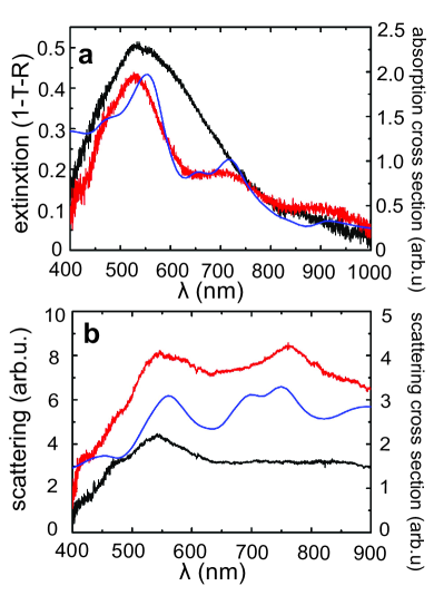
The measurements of extinction (Fig. 4a) and scattering (Fig. 4b) spectra from ordered 330-nm nanoparticles (Fig. 2b,d) array revealed two resonances at 530 nm and 750 nm (for the measurements details see Methods). These resonances are in good qualitative agreement with our numerical simulation (Fig. 4a,b) for array of gold 330-nm spheres embedded on half in fused silica infinite substrate (for calculation details see Methods). According to our simulations, the ”green” and ”red” maxima correspond to quadrupole and dipole plasmon resonances, respectively. It is worth noting that in comparison with ordered monodisperse nanoparticles fabricated under optimal conditions (h=30 nm, P=1 m), the disordered nanoparticles (h=30 nm, P=0.7 m) with wide size distribution (from sub-100 nm up to 0.5 m) exhibit single and broad extinction resonance. Indeed, sub-100 nm nanoparticles agglomerates surround each hundreds-nm particle (Fig. 2c), providing additional strong dipole resonance contribution into scattering/absorbtion spectra in the range of =500–600 nm.
In order to show the applicability of the novel method of large-scale Au nanoparticles array fabrication, we measured Raman scattering signal from deposited molecules of rhodamine-6G (R6G) on the nanostructured substrates (for the measurements details, see Methods). The typical Raman scattering spectra from a single layer of R6G on different fs-laser fabricated substrates with Au nanoparticles are shown in Fig. 5a. The systematic study of SERS signal on scan periods reveals its strong dependence on the type of nanostructures. The relatively low average enhancement factor (EF) corresponds to both micro-patches and ordered nanoparticles fabricated at cross-scan periods P 0.7m, being approximately one order of magnitude higher than SERS signal from R6G on a smooth Au film (Fig. 5b). Nevertheless, these structures exhibit up to 5-fold higher than a smooth Au 30-nm film with roughness amplitude less than 1 nm, which provides the so-called chemical mechanism of SERS and weak electromagnetic contribution on the roughness Moskovits (1985). The surface of the structures is not planar, and the main contribution to Raman signal gives R6G molecules from ordered Au nanoparticles with surface area of four times smaller than area of smooth substrate surface within laser spot. Taking into account this fact, the SERS signal for the ordered array of the nanoparticles is about one order of magnitude larger in comparison with the signal on the film. Our numerical modeling of the electric field distribution nearby a single 330-nm Au nanoparticle embedded in fused silica shows the highest value lower than 100 in the hot spots, providing 3-fold electric field enhancement ().
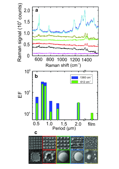
The strongest average enhancement factor is observed on structured 30-nm film at scan periods of 0.7 m and 0.8 m, where extremely hot spots are formed in the gaps within conglomerates of sub-100 nm nanoparticles (see the SEM images in deep blue frames in Fig. 5c). Our SEM images reveal only 102 pairs of the sub-100-nm nanoparticles separated on a few nanometers nearby each 330-nm Au nanoparticle Fig. 2c, 5c). Therefore, one can assume that only 103–104 molecules from these gaps contribute to the average 105 over whole laser spot with 1.1106 molecules, resulting in local in the gaps up to 109–1010. Indeed, our numerical calculations of two touching gold 20-nm nanoparticles provide electric-field maximum enhancement at =633 nm in the range of 10–20 in place of fitting of 1.5-nm R6G molecule between the particles, resulting in electric-field contribution to SERS local enhancement factor of 105. Since the estimated chemical contribution to SERS from measurements of Raman signal of R6G on thin Au 30-nm film lies in the range of (5–9)103, the total EF in the gap can achieve the level of 109, which is comparable with previous reports García-Vidal and Pendry (1996); Ward et al. (2007); Ye et al. (2012).
In conclusion, the developed novel single-step and lithography-free method of direct Au-nanoparticles fabrication opens new possibilities to fabricate 0D, 1D, and 2D plasmonic nanostructures on large-scale. To the best of our knowledge, it is the first demonstration of simultaneous cutting and dewetting of thin metallic film processes that paves the way to extremely simplify the technology of monodisperse and ordered nanoparticles fabrication. The systematic experimental study reveals at least two functional regimes of film patterning: for light filtering and sensing. We believe that the applications range of this simple and low-cost method will be extended soon to nonlinear optical problems as well as various chemical and biomedical applications.
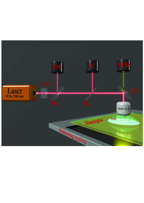
Methods. Fabrication. A commercial femtosecond laser system (Femtosecond Oscillator TiF- 100F, Avesta Poject) was used, providing laser pulses at 780 nm central wavelength, with maximum pulse energy of 5 nJ, and pulse duration of 50 fs at the repetition rate of 80 MHz. Laser energy was varied and controlled by an acousto-optical modulator (R23080-3-LTD, Gooch and Housego) and a power meter (FielfMax II, Coherent), respectively, while the pulse duration was measured by an autocorrelator (Avesta Poject). Detailed experimental setup is presented in Supplementary Materials (Fig.S1).
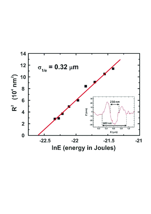
Laser pulses were tightly focused by an oil immersion microscope objective (Carl Zeiss 100) with a numerical aperture (NA) of 1.4 (experimental setup is shown in Supplementary Information). According to the relation d1.22/NA, the estimated full-width at half-maximum diameter of the beam focal spot size is =0.68 m, which is close to measured value (0.64 m) by standard method Liu (1982) based on the dependence of laser-damaged area on incident laser energy (for details, see the Supplementary Information).
Laser beam was focused on supported Au films with thicknesses in the range of =10–60 nm, thermally evaporated (Bock Edwards Auto 500) on the back side of 140-m-thick silica glass without any additional adhesion-improving layers. The samples were then placed on a three-dimensional air-bearing translating stage driven by brushless servomotors (ABL1000, Aerotech), allowing sample translation with various scan speeds up to 300 mm/s. In all experiments, film surface scanning by the laser beam was carried out with velocity of 5 mm/s, providing the number of laser pulses per each point of approximately .
Characterizations. Preliminary optical imaging of the structured films was provided immediately during the laser processing by integrated CCD camera, collecting transmitted through the film white light from a lamp (Fig.S1). The high-resolution morphology characterization was carried out by means of scanning electron microscope (SEM, Carl Zeiss, Neon 40) and atomic force microscope (AFM, SmartSPM AIST-NT). The Fourier spectra of SEM images were obtained in ImajeJ software.
Optical transmission (T) and reflection (R) broadband measurements were carried out at normal incidence of linearly polarized light from a halogen lamp (HL-2000-FHSA), using a commercial spectrometer (Horiba LabRam HR) with CCD camera (Andor DU 420A-OE 325). The excitation Olympus PlanFI (NA=0.95) and collection Mitutoyo M Plan APO NIR (NA=0.7) objectives were used for transmission measurements. Objective Mitutoyo M Plan APO NIR (NA=0.42) was employed for reflection measurements. Scattering (S) spectra measurements were carried out in a dark-field scheme, where the arrays irradiation was performed at an angle of incidence of 78∘ with surface normal and scattered signal collection was performed by means of objective Mitutoyo M Plan APO NIR (NA=0.7). Confocal optical scheme was optimized for collection of all signals (T,R and S).
SERS measurements and enhancement factor calculations. The nanoparticles were functionalized with a selfassembled monolayer of R6G. The substrates were submerged in 0.5-mM solution made with water for 1 hour and then gently rinsed in neat water. Enhancement factor estimates were measured on a micro-Raman apparatus (Raman spectrometer HORIBA LabRam HR, AIST SmartSPM system). Using a 15-mW, 632.8-nm HeNe laser, spectra were recorded through the 50 microscope objective (NA=0.42) and projected onto a thermoelectrically cooled charge-coupled device (CCD, Andor DU 420A-OE 325) array using a 600-g/mm diffraction grating. Individual spectra were recorded from both single spots (1.8-m diameter) on the substrates, and from a 1-cm thick cell of neat R6G for normalization.
From these measurements, the averaged over the excitation beam size Raman scattering enhancement factor (EF) for the substrate is estimated with , where and are the intensities of a specific Raman band, respectively. Two Raman modes of R6G at 612 cm-1 and 1360 cm-1 were chosen for the EF calculations. The number of probed molecules in the unenhanced sample of neat R6G, , is approximated using the molecular weight and density of R6G and the effective interaction volume of the Gaussian laser beam with the neat R6G sample. To estimate the , we calculated the effective excitation volume by using the equation: , where r is the radius of the beam size (0.9 m) and H is the effective depth of focus (9 m). Thus, we estimated an effective excitation volume of 22.9 for our Raman microscopy with 633 nm excitation using the objective. Then, was calculated by the expression: molecules, where is the concentration (), is the density of R6G (1.26 g/cm3), M is the molar mass of R6G (479 g/mol) and is the Avogadro constant (6.021023 mol-1). To determine , a self-assembled monolayer of R6G molecules (molecular footprint size of SR6G2.2 nm2 Gupta and Weimer (2003)) was assumed to be closely packed on the surface and the number of the molecules within focused beam can be estimated as N=r2/SR6G1.1106.
Numerical Simulations. Numerical simulations are performed by using both frequency-domain and time-domain solvers in the commercial software CST Microwave Studio. Incidence of a plane wave at given wavelength on a gold Palik (1998) sphere of a given radius embedded on half in fused silica (=2.1) infinite substrate is considered.
Acknowledgments
This work was financially supported by Russian Science Foundation (Grant 15-19-00172). The authors are thankful to Prof. Y.S. Kivshar, Prof. S.I. Kudryashov, and M. Hasan for discussions.
References
- Maier (2007) S. A. Maier, Plasmonics: fundamentals and applications (Springer Science : Business Media, 2007).
- Luk’yanchuk et al. (2010) B. Luk’yanchuk, N. I. Zheludev, S. A. Maier, N. J. Halas, P. Nordlander, H. Giessen, and C. T. Chong, Nature materials 9, 707 (2010).
- Kravets et al. (2008) V. Kravets, F. Schedin, and A. Grigorenko, Phys. Rev. Lett. 101, 087403 (2008).
- Liu et al. (2008) Z. Liu, A. Boltasseva, R. H. Pedersen, R. Bakker, A. V. Kildishev, V. P. Drachev, and V. M. Shalaev, Metamaterials 2, 45 (2008).
- Yu and Capasso (2014) N. Yu and F. Capasso, Nature Materials 13, 139 (2014).
- Maier et al. (2003) S. A. Maier, P. G. Kik, H. A. Atwater, S. Meltzer, E. Harel, B. E. Koel, and A. A. Requicha, Nature Materials 2, 229 (2003).
- Moskovits (1985) M. Moskovits, Rev. Mod. Phys. 57, 783 (1985).
- Lal et al. (2007) S. Lal, S. Link, and N. J. Halas, Nature Photonics 1, 641 (2007).
- Anker et al. (2008) J. N. Anker, W. P. Hall, O. Lyandres, N. C. Shah, J. Zhao, and R. P. Van Duyne, Nature Materials 7, 442 (2008).
- Kauranen and Zayats (2012) M. Kauranen and A. V. Zayats, Nature Photonics 6, 737 (2012).
- Lee et al. (2014) J. Lee, M. Tymchenko, C. Argyropoulos, P.-Y. Chen, F. Lu, F. Demmerle, G. Boehm, M.-C. Amann, A. Alù, and M. A. Belkin, Nature 511, 65 (2014).
- Minovich et al. (2015) A. E. Minovich, A. E. Miroshnichenko, A. Y. Bykov, T. V. Murzina, D. N. Neshev, and Y. S. Kivshar, Laser Photonics Rev. 9, 195 (2015).
- Junno et al. (1995) T. Junno, K. Deppert, L. Montelius, and L. Samuelson, Appl. Phys. Lett. 66, 3627 (1995).
- Kraus et al. (2007) T. Kraus, L. Malaquin, H. Schmid, W. Riess, N. D. Spencer, and H. Wolf, Nature Nanotech. 2, 570 (2007).
- Shi et al. (2013) L. Shi, J. T. Harris, R. Fenollosa, X. Rodriguez, I.and Lu, B. A. Korgel, and F. Meseguer, Nature Comm. (2013).
- Patra et al. (2014) P. P. Patra, R. Chikkaraddy, R. P. Tripathi, A. Dasgupta, and G. P. Kumar, Nature Comm. 5 (2014).
- Bischof et al. (1996) J. Bischof, D. Scherer, S. Herminghaus, and P. Leiderer, Phys. Rev. Lett. 77, 1536 (1996).
- Higgins and Jones (2000) A. M. Higgins and R. A. Jones, Nature 404, 476 (2000).
- Abbarchi et al. (2014) M. Abbarchi, M. Naffouti, B. Vial, A. Benkouider, L. Lermusiaux, L. Favre, A. Ronda, S. Bidault, I. Berbezier, and N. Bonod, ACS Nano 8, 11181 (2014).
- Trice et al. (2007) J. Trice, D. Thomas, C. Favazza, R. Sureshkumar, and R. Kalyanaraman, Phys. Rev. B 75, 235439 (2007).
- Wu et al. (2011) Y. Wu, J. D. Fowlkes, and P. D. Rack, J. Mater. Res. 26, 277 (2011).
- Lian et al. (2006) J. Lian, L. Wang, X. Sun, Q. Yu, and R. C. Ewing, Nano Lett. 6 (2006).
- Kuznetsov et al. (2009) A. Kuznetsov, J. Koch, and B. Chichkov, Opt. Express 17, 18820 (2009).
- Kuznetsov et al. (2011) A. I. Kuznetsov, A. B. Evlyukhin, M. R. Gonçalves, C. Reinhardt, A. Koroleva, M. L. Arnedillo, R. Kiyan, O. Marti, and B. N. Chichkov, ACS Nano 5, 4843 (2011).
- Zywietz et al. (2014) U. Zywietz, A. B. Evlyukhin, C. Reinhardt, and B. N. Chichkov, Nature Comm. 5 (2014).
- Ionin et al. (2015) A. Ionin, S. Kudryashov, S. Makarov, A. Rudenko, Y. N. Kulchin, O. Vitrik, T. Efimov, and A. Kuchmizhak, Opt. Lett. 40, 224 (2015).
- Zhigilei et al. (2009) L. V. Zhigilei, Z. Lin, and D. S. Ivanov, J. Phys. Chem. C 113, 11892 (2009).
- Bauerle (2011) D. W. Bauerle, Laser processing and chemistry (Springer Science & Business Media, 2011).
- Gadkari et al. (2005) P. Gadkari, A. Warren, R. Todi, R. Petrova, and K. Coffey, J. Vac. Sci. Tech. A 23, 1152 (2005).
- Kim et al. (2009) D. Kim, A. L. Giermann, and C. V. Thompson, Appl. Phys. Lett. (2009).
- Fowlkes et al. (2011) J. D. Fowlkes, L. Kondic, J. Diez, Y. Wu, and P. D. Rack, Nano Lett. 11, 2478 (2011).
- Wu et al. (2014) Y. Wu, N. Dong, S. Fu, J. D. Fowlkes, L. Kondic, M. A. Vincenti, D. de Ceglia, and P. D. Rack, ACS Appl. Mater. Interfaces 6, 5835 (2014).
- Fowlkes et al. (2014) J. Fowlkes, N. Roberts, Y. Wu, J. Diez, A. Gonzalez, C. Hartnett, K. Mahady, S. Afkhami, L. Kondic, and P. Rack, Nano Lett. 14, 774 (2014).
- Thompson (2012) C. V. Thompson, Annu. Rev. Mater. Res. 42, 399 (2012).
- Landau and Lifshitz (1987) L. Landau and E. Lifshitz, Fluid Mechanics, 2nd ed. (Butterworth-Heinemann, 1987) p. 551.
- Wyart and Daillant (1990) F. B. Wyart and J. Daillant, Can. J. Phys. 68, 1084 (1990).
- García-Vidal and Pendry (1996) F. García-Vidal and J. Pendry, Phys. Rev. Lett. 77, 1163 (1996).
- Ward et al. (2007) D. R. Ward, N. K. Grady, C. S. Levin, N. J. Halas, Y. Wu, P. Nordlander, and D. Natelson, Nano Lett. 7, 1396 (2007).
- Ye et al. (2012) J. Ye, F. Wen, H. Sobhani, J. B. Lassiter, P. V. Dorpe, P. Nordlander, and N. J. Halas, Nano Lett. 12, 1660 (2012).
- Liu (1982) J. Liu, Opt. Lett. 7, 196 (1982).
- Gupta and Weimer (2003) R. Gupta and W. Weimer, Chem. Phys. Lett. 374, 302 (2003).
- Palik (1998) E. D. Palik, Handbook of optical constants of solids (Academic press, 1998).
Supplementary materialss:
Simple Method for Large-Scale Fabrication of Plasmonic Structures
Our experimental setup for laser ablation is schematically illustrated in Fig. 6.
The method of beam size measurement Liu (1982) is based on approximation of used focused laser beam by Gaussian spatial distribution for fluence , where r is the distance from the beam center, is the Gaussian beam size on the 1/e-level. Since the ablation threshold is a constant for given film and the number of pulses, the dependence of damaged area radii (R) on laser energy also can be fitted by Gaussian function, which is linear in -lnE coordinates (Fig. 7).