Clean carbon nanotubes coupled to superconducting impedance-matching circuits
Abstract
Coupling carbon nanotube devices to microwave circuits offers a significant increase in bandwidth and signal-to-noise ratio. These facilitate fast non-invasive readouts important for quantum information processing, shot noise and correlation measurements. However, creation of a device that unites a low-disorder nanotube with a low-loss microwave resonator has so far remained a challenge, due to fabrication incompatibility of one with the other. Employing a mechanical transfer method, we successfully couple a nanotube to a gigahertz superconducting matching circuit and thereby retain pristine transport characteristics such as the control over formation of, and coupling strengths between, the quantum dots. Resonance response to changes in conductance and susceptance further enables quantitative parameter extraction. The achieved near matching is a step forward promising high-bandwidth noise correlation measurements on high impedance devices such as quantum dot circuits.
Artificial two-level systems such as Josephson junction qubits coupled to superconducting microwave cavities Wallraff2004 ; Clarke2008 have allowed for unprecedented break-throughs in quantum information processing. Inspired by these results, other solid state systems have been coupled to resonant circuits, such as double quantum dots in semiconductors Frey2012 ; Toida2013 ; Petersson2012 ; Deng2013 ; Viennot2014 as potential qubits, and molecules or impurity spin ensembles Rabl2006 ; Kubo2010 ; Schuster2010 ; Wu2010 as quantum memories. In particular, carbon nanotubes (CNT) have recently demonstrated their potential as low disorder one-dimensional electron systems Pei2012 ; Waissman2013 ; Jung2013 , which have been used to probe the physics of spin-orbit Kuemmeth2008 and electron-phonon coupling Benyamini2014 as well as to perform initialization and manipulation of spin qubits Laird2013 . Carbon nanotubes suspended over local gates not only offer a decoupling from the surface but also mechanical resonances with high quality factors Huttel2009 , creation of arbitrary local potentials and tight confinement with charging energies in excess of 50 meV Jung2013 .
Nevertheless, coupling CNTs to half-wave resonators Delbecq2011 ; Delbecq2013 ; Viennot2014 and other types of circuits Roschier2004 ; Tang2007 ; Lechner2010 ; Chorley2012 faces a significant challenge: achieving a low microwave loss device while preserving the ideal transport characteristics of pristine CNTs in a geometry which allows full control over charge confinement. While CNT devices with clean transport spectra can be obtained using a growth-last approach Cao2005 , the low yield and high temperatures () involved prohibit the use of this method for fabricating superconductor-CNT hybrid devices. Recently, the transfer of CNTs from a growth substrate to a separate microwave device, followed by standard lithography has been demonstrated Viennot2014a , solving issues with material compatibility but not addressing limited yield and unclean transport spectra. As such, the combination of low loss microwave circuits with clean CNTs has not been achieved so far, impeding the way toward experiments involving the interplay of electrons in CNTs with microwave photons.
Here, we couple a locally tunable suspended CNT quantum device to an impedance-matching circuit based on superconducting transmission lines. Different to previous works Delbecq2011 ; Delbecq2013 ; Viennot2014 where half wave resonators are employed for dispersive and a minimal invasive measurement, our circuit is aimed at providing an efficient channel to transfer (collect) microwave radiation into (from) a quantum device. Additionally, the circuit offers bandwidths (BW) in the MHz range even for device impedances on the
order of 1M. These features, on one hand, allow us to perform high BW measurements for deducing both conductance and susceptance changes in the quantum device at GHz frequencies, and on another hand, provide near unity collection of emitted radiation power for fast shot noise measurements. Through a mechanical transfer process Muoth2013 , we place the CNT on the finished microwave device in the last step. Such a selective assembly technique Waissman2013 allows us to address the mentioned fabrication and yield issues while obtaining clean transport spectra in combination with low microwave loss circuits. We employ local gates to demonstrate a high degree of control over the formation of double dots in the ambipolar regime and perform RF measurements of the device susceptibility. We are able to tune the inter-dot coupling strength and extract values on the order of using the phase response of the microwave circuit. By performing simultaneous measurements of resistance and complex impedance, we observe good quantitative agreement between DC conductance and RF measurements.
Results
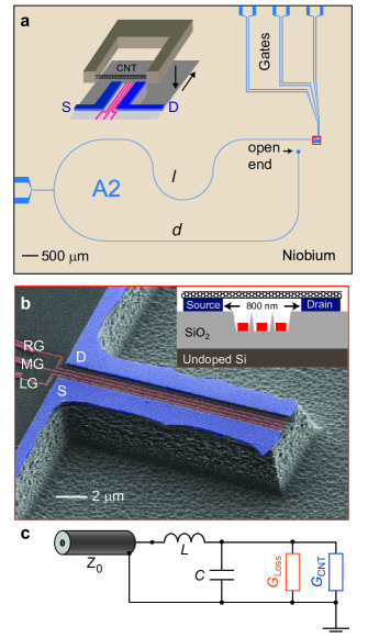
Mechanical transfer of CNT. A key advance in this hybrid-CNT device is the implementation of a mechanical transfer at ambient conditions. The same marks the last step of sample fabrication. After the complete RF and DC circuitry are fabricated, the chip is bonded on a printed circuit board and cleaned with a weak argon plasma to remove oxides and fabrication residue from the contacts. We grow CNTs on the fork-like structures of a separate chip, which allow a resist- and ebeam radiation free mechanical transfer of the CNTs to the source/drain electrodes on a pillar structure (inset Fig. 1a). Forks are aligned with the pillar using an optical microscope of a micro-manipulator setup and successful transfers are monitored through voltage biased (200 mV) resistance measurements. We can then determine bandgap characteristics of transferred CNTs by measuring the conductance response to an applied gate voltage. Furthermore, we can remove tubes with unwanted characteristics, such as a metallic response, by applying a large bias voltage, and subsequently transfer and test another CNT on the same device. These capabilities make our method of transfer a deterministic one with unity device yield. Further details of the CNT growth and transfer method can be found in the Supplementary Note 2.
Combining superconducting impedance matching circuits with gate controlled CNT devices. A transmission line based impedance matching circuit, termed stub tuner Pozar05 , can be realized by two transmission lines connected in parallel, with the device placed on one end, the other ending in an open circuit (Fig. 1a). Though simple lumped circuits can also be employed, they demand a lengthy iterative design procedure when used at frequencies of GHz due to stray capacitances fF. By utilizing transmission lines, we are not only able to minimize parasitic effects, such as stray capacitances, but are also able to compensate for them, as they only change the effective length of the lines.
The microwave response of the stub tuner is mainly determined by the lengths of the two lines and , which are chosen such that a specific device impedance, called the matched load , will be transformed to the characteristic impedance of the line at one specific resonance frequency. At this load, the reflection coefficient is minimized, implying maximum power transfer. To get the reflectance , we calculate the impedance of the hybrid device, consisting of a parallel combination of the two transmission lines Pozar05 ; Gabriel2012 as
| (1) |
is the propagation constant with and being the loss and phase constants respectively, the effective dielectric constant, the speed of light, the frequency, the transmission line impedance, and the complex admittance with conductance, and susceptance of the CNT device.
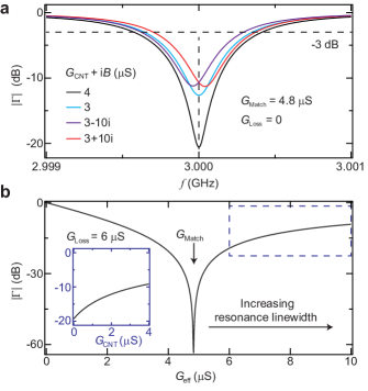
The circuit is sensitive to changes in both the conductance and susceptance, as shown in Fig. 2a, where we plot a set of reflection spectra for different load admittances , with lengths chosen for a resonance at 3 GHz and a matched load of S, assuming no losses. Varying from to increases both the depth and width of the resonance, but not the resonance frequency. In contrast, a change in the susceptance mainly shifts the resonance, with a minor change in its depth. To illustrate the effects that losses have on this device, we can replace the circuit by an equivalent lossless one while introducing a phenomenological conductance parallel to the CNT load (Fig. 1c) and thus defining a total effective load seen by the microwaves. In Fig. 2b, we plot at the resonance as a function of . The reflected signal is the smallest close to the matched load offering maximal power transfer. The latter is more important for measuring small noise-power emitted from the device. Due to the additional loss conductance , the CNT load which matches the circuit is smaller than and given by . In particular, if full matching is precluded and the reflection coefficient as a function of load becomes monotonic (see inset of Fig. 2b).
The presented CNT device has three recessed local bottom gates with additional source and drain contacts elevated by nm (Fig. 1b). Bottom gates are separated by nm from each other and from the source drain contacts producing a suspended length of the CNT of nm. The transmission lines are patterned on a Nb film and yield a resonance frequency . All measurements are performed at the base temperature of the cryostat mK (Supplementary Note 3). The source is connected to the central conductor of the transmission line ( branch) while the drain is connected to the ground plane. For the characterization of the devices, the CNT is tuned into the bandgap to present an infinite resistance and hence an open end. By measuring the reflection spectrum, it is possible to extract the relevant parameters ( and ). The extracted loss for probe power in the range [-110,-140] dBm corresponds to internal quality factors of 10,000 to 9000 for an equivalent half-wave resonator, showing that we are able to achieve low-loss microwave circuits in combination with CNT devices. Due to parasitic inductances from the fabricated contacts, the matching circuit has a lower effective S compared to S and operates therefore in the internal-loss-dominated regime. Measurements of the matching circuit response can be found in the Supplementary Note 4, as well as the measurement of an additional sample where full matching is demonstrated (Supplementary Note 5).
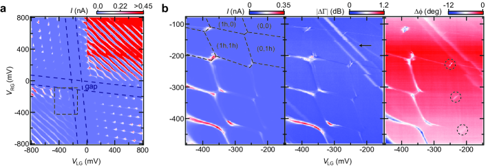
Locally tunability and RF reflectometry measurements of CNT double quantum dots. Room temperature DC characterization during the device assembly allows us to perform several CNT mechanical transfer trials on the same device and choose nanotubes based on their gate dependence. In particular for semiconducting nanotubes, we can use the bottom gates to locally shift the Fermi level above or below the valence and conduction bands of the nanotube. The latter allows for creating gate-defined confinement potentials along the nanotube and hence for tuning the location, size and number of quantum dots Waissman2013 . With no RF power applied to the stub tuner and the middle gate V, we first measure the charge stability diagram of the CNT device. A gate sweep using left () and right gates () at DC bias is shown in the Fig. 3a. The current response clearly displays the ambipolar behavior of quantum dots around a semiconducting gap of with left and right gates tuning the CNT into n-n, n-p, p-n and p-p double dots. Here we have used a gate lever arm of meV/mV extracted from the Coulomb diamond measurements. In addition, we observe the exact charge occupation of electrons and holes at corresponding gate voltages Pei2012 . The high conductance in the n-n regime is possibly due to n-doping near the source/drain contacts. We also found p-doping for many samples for the same Pd contacts and do not exactly understand the nature of the observed contact doping.
We now perform simultaneous measurements of DC and RF reflectometry to obtain a collective response of the double quantum dots. is measured near the resonance frequency with a probe power chosen to be so low that no out-of-equilibrium charges are induced when applying microwave signal to the stub tuner. Figure 3b shows a qualitatively similar honeycomb charge stability diagram in current, amplitude and phase responses taken at mV bias. We clearly observe co-tunneling lines Frey2012 , long edges of the honeycomb, in all plots suggesting good sensitivity to impedance changes even in case of a circuit whose internal losses dominate the quality factor of the resonances. Here, we note an important distinction of the stub tuner. For half wave resonators, RF signal for co-tunneling lines strongly depend on strength of capacitive coupling to respective lead-dot transitions and their rates with respect to the resonance frequency Frey2012b . DC coupled stub tuner in contrast still responds through conductance changes that provide an external coupling by shunting microwaves via drain contact into the ground plane. This is further seen in Fig. 3b where larger current results in larger and (see Supplementary Fig. 3a, 3b). In addition, we also observe hybridized double dots at degeneracy, the boundary of two honeycombs at the two smaller edges, marked by dashed circles in Fig. 3b, in the phase and amplitude plots. The signal results from the susceptance changes caused by dipole coupling of the hybridized charge states to the microwave resonance. The responses at different charge degeneracies are different due to the distinct dot coupling energies which are affected by all gate voltages in our sample.
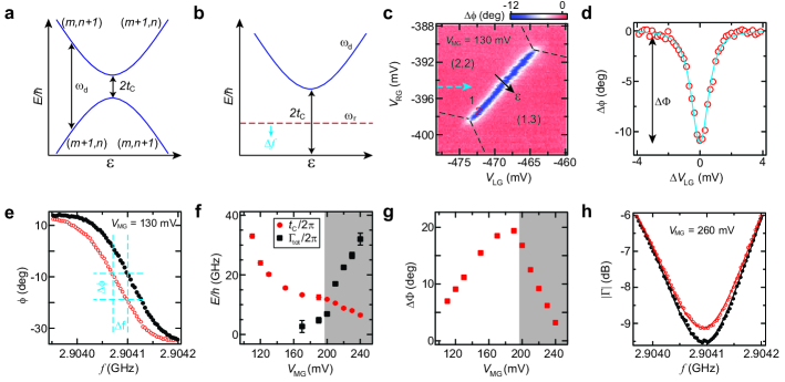
To illustrate the control over the confinement potential of the double quantum dots in this clean CNT device, is used to tune the tunneling barrier between the two quantum dots. In the DC measurements, the strength of the tunneling coupling is visible as the separation between the charge triple points with the larger value corresponding to a stronger coupling or weaker barrier (Supplementary Fig. 5). For a quantitative analysis, the phase response of the stub tuner can be measured using a weak probe power (-130 dBm) near the hybridization of two charge states and as shown in Fig. 4a. We operate in the zero-bias regime, allowing the dots to stay in equilibrium and rule out any conductance changes which could affect the resonance response. Such a phase shift is shown in Fig. 4c close to (2,2) to (1,3) hole transition. We infer the frequency shifts from the phase variations which are almost linearly correlated near resonance [see Fig. 4e, error in our case]. Following a semiclassical model describing the coupling of a qubit with frequency to a resonator with frequency (Supplementary Note 7), the dispersion of the resonator is given by
| (2) |
where with and the effective relaxation and dephasing rates of the hybridized double dot respectively, and being the detuning, the zero temperature coupling strength with the resonator and the polarization of the double dot transition at electronic temperature . We use the equation to first extract in a regime where is large ( is small) so that , . This yields a dependence of the frequency shift proportional to , now independent of . A fit with this equation to the data at mV is shown in Fig. 4d, yielding . We find the same for mV supporting the assumption that is relatively small in this regime. Fixing this for phase responses at other , we plot the extracted and in Fig. 4f and observe a reduction of on increasing reflecting a reduction in the tunnel coupling strength between the dots. The phase response starts to be suppressed for larger than due to increasingly fast double dot relaxation, yielding . The inverse dependence of on has been seen in similar systems Basset2013 ; Viennot2014 and could be due to the charge noise environment Petersson2010 of the nanotube. The sign of the frequency shift always remains negative, further signifying that the resonator energy is always smaller than . Increasing to more than , we do not notice any dispersion because of the large . However, the hybridized dots still show a response similar to Fig. 2a, now only in the reflectance amplitude. For , the stub tuner response for coupled and uncoupled dots regimes is presented in Fig. 4h. The fit to the resonance at the double dot degeneracy (open circles) shows a smaller depth and m-1 compared to the one in the uncoupled regime (solid circles) with m-1. This behavior is a result of an added loss channel i.e. absorption from the two-level hybridized dots when becomes comparable to , which is also consistent with the change in the resonance depth due to the conductance increase for our device parameters (Supplementary Fig. 3a, 6b).
Discussion
In summary, we have operated a RF superconducting impedance-matching circuit to measure CNT quantum dots in a hybrid device fabricated using a mechanical transfer of CNTs. The transfer employed here not only allows for a deterministic assembly and unity yield of complex RF devices, but also for the selection of CNTs with specific properties (metallic or semi-conducting), reuse of the same circuit with different tubes and incorporation of desirable contact materials. We demonstrate the ability to locally control the confinement potential along the length of the suspended nanotube and to form dots with a precise number of charges. The high symmetry in the ambipolar charge stability around the bandgap indicates low disorder in the CNT system.
Additionally, the matching circuit enables a comparatively simple extraction of the RF device impedance. We have shown that one can quantitatively deduce admittance changes in S resolution by measuring the complex reflectance . This sensitivity can be used to deduce basic parameters of a clean CNT double-dot operating as a charge qubit, such as the interdot tunnel coupling strength and the relaxation rate. More importantly, conductances can be deduced using a simple analytic formula with measurement BW reaching estimated using eq. 1 near matching. We show an extraction of from the RF amplitude response for a similar device, now at full matching, in the Supplementary Note 5. We find Coulomb diamond plots quantitatively similar to its DC counterpart and demonstrate a BW up to 2 MHz and a reflectance down to -40 dB for device S. The reliable high-bandwidth extraction of at GHz frequencies holds promises for probing quantum charge-relaxation resistance, which can deviate from its usual DC counterpart described by the Landauer formula Buttiker1993 ; Gabelli2006 .
We demonstrate near matching with a substantial in and out microwave coupling in the measured device. For example, we see from Supplementary Fig. 3a that we achieve dB at S. This relates to a reflectance probability of 16 , hence 84 is transmitted into the matching circuit and CNT device. Taking into account the internal loss described by S yields a substantial power transmission of from a M device to a transmission line. This is beneficial for high throughput detection of emission noise from the quantum device defined in the CNT wire and shot noise measurements Schoelkopf1998 . The presented ability to combine an intricate RF circuit with a pristine suspended CNT will invite novel studies on devices with engineered mechanical, electrical and photonic degrees of freedom.
Methods
Sample fabrication. The device is patterned on a 150 nm thick Nb film, sputtered on an undoped Si substrate with 170 nm of , using photolithography and subsequent dry etching. The center conductor of the transmission line is m wide, while gaps are m wide, yielding a calculated . The geometric lengths and of the stub tuner are 10.66 mm and 10.36 mm respectively. Spurious modes due to the T-junction are suppressed using on-chip wire bonds. The local bottom gates (Ti/Au of 5/35 nm thickness and 60 nm width) are defined by electron beam lithography and recessed in the using dry anisotropic and isotropic etching with and Ar/, respectively (total recess depth 100 nm). A recess of depth m is etched via dry etching with around the Pd (100 nm) contacts to facilitate mechanical transfer Muoth2013 . A modified micro-manipulator is used for CNT transfer at ambient conditions using optical microscopy. Contact resistances of CNT are generally found in excess of Waissman2013 , which may be attributable to remaining oxide on the contacts and contact geometry. We obtained yield of transferring a single tube. More than one tube transferred at the same time due to multiple tubes on the same fork showed high conductance and could be removed by applying a large source drain bias.
Data Analysis. We extract the relevant parameters such as of the device by fitting the resonance at zero conductance using the following equation
| (3) |
where the phase factor accounts for impedance mismatches in the setup and for an offset. We could not exactly
determine the electronic temperature of the device and assume for all fits in Fig. 4d. For ,
extraction of relatively smaller is unreliable due to large detuning from the stub tuner resonance.
References
- (1) Wallraff, A. et al. Strong coupling of a single photon to a superconducting qubit using circuit quantum electrodynamics. Nature 431, 162–167 (2004).
- (2) Clarke, J. & Wilhelm, F. K. Superconducting quantum bits. Nature 453, 1031 (2008).
- (3) Frey, T. et al. Dipole coupling of a double quantum dot to a microwave resonator. Phys. Rev. Lett. 108, 046807 (2012).
- (4) Toida, H., Nakajima, T. & Komiyama, S. Vacuum rabi splitting in a semiconductor circuit qed system. Phys. Rev. Lett. 110, 066802 (2013).
- (5) Petersson, K. D. et al. Circuit quantum electrodynamics with a spin qubit. Nature 490, 380–383 (2012).
- (6) Deng, G. W. et al. Circuit qed with a graphene double quantum dot and a reflection-line resonator. Preprint at arXiv:1310.6118 (2013).
- (7) Viennot, J. J., Delbecq, M. R., Dartiailh, M. C., Cottet, A. & Kontos, T. Out-of-equilibrium charge dynamics in a hybrid circuit quantum electrodynamics architecture. Phys. Rev. B 89, 165404 (2014).
- (8) Rabl, P. et al. Hybrid quantum processors: Molecular ensembles as quantum memory for solid state circuits. Phys. Rev. Lett. 97, 033003 (2006).
- (9) Kubo, Y. et al. Strong coupling of a spin ensemble to a superconducting resonator. Phys. Rev. Lett. 105, 140502 (2010).
- (10) Schuster, D. I. et al. High-cooperativity coupling of electron-spin ensembles to superconducting cavities. Phys. Rev. Lett. 105, 140501 (2010).
- (11) Wu, H. et al. Storage of multiple coherent microwave excitations in an electron spin ensemble. Phys. Rev. Lett. 105, 140503 (2010).
- (12) Pei, F., Laird, E. A., Steele, G. A. & Kouwenhoven, L. P. Valley-spin blockade and spin resonance in carbon nanotubes. Nat Nano 7, 630–634 (2012).
- (13) Waissman, J. et al. Realization of pristine and locally tunable one-dimensional electron systems in carbon nanotubes. Nat Nano 8, 569–574 (2013).
- (14) Jung, M. et al. Ultraclean single, double, and triple carbon nanotube quantum dots with recessed re bottom gates. Nano Letters 13, 4522–4526 (2013).
- (15) Kuemmeth, F., Ilani, S., Ralph, D. C. & McEuen, P. L. Coupling of spin and orbital motion of electrons in carbon nanotubes. Nature 452, 448–452 (2008).
- (16) Benyamini, A., Hamo, A., Kusminskiy, S. V., von Oppen, F. & Ilani, S. Real-space tailoring of the electron-phonon coupling in ultraclean nanotube mechanical resonators. Nat Phys 10, 151–156 (2014).
- (17) Laird, E. A., Pei, F. & Kouwenhoven, L. P. A valley-spin qubit in a carbon nanotube. Nat Nano 8, 565–568 (2013).
- (18) Huttel, A. K. et al. Carbon nanotubes as ultrahigh quality factor mechanical resonators. Nano Letters 9, 2547–2552 (2009).
- (19) Delbecq, M. R. et al. Coupling a quantum dot, fermionic leads, and a microwave cavity on a chip. Phys. Rev. Lett. 107, 256804 (2011).
- (20) Delbecq, M. et al. Photon-mediated interaction between distant quantum dot circuits. Nat Commun 4, 1400– (2013).
- (21) Roschier, L. et al. Carbon nanotube radio-frequency single-electron transistor. Journal of Low Temperature Physics 136, 465–480 (2004).
- (22) Tang, Y., Amlani, I., Orlov, A. O., Snider, G. L. & Fay, P. J. Operation of single-walled carbon nanotube as a radio-frequency single-electron transistor. Nanotechnology 18, 445203 (2007).
- (23) Lechner, L. G., Wu, F., Danneau, R., Andresen, S. E. & Hakonen, P. RF-electrometer using a carbon nanotube resonant tunneling transistor. J. App. Phys. 107, 084316 (2010).
- (24) Chorley, S. J. et al. Measuring the complex admittance of a carbon nanotube double quantum dot. Phys. Rev. Lett. 108, 036802 (2012).
- (25) Cao, J., Wang, Q. & Dai, H. Electron transport in very clean, as-grown suspended carbon nanotubes. Nat Mater 4, 745–749 (2005).
- (26) Viennot, J. J., Palomo, J. & Kontos, T. Stamping single wall nanotubes for circuit quantum electrodynamics. Applied Physics Letters 104, – (2014).
- (27) Muoth, M., Chikkadi, K., Liu, Y. & Hierold, C. Suspended cnt-fet piezoresistive strain gauges: Chirality assignment and quantitative analysis. In Micro Electro Mechanical Systems (MEMS), 2013 IEEE 26th International Conference on, 496–499 (2013).
- (28) Pozar, D. M. Microwave Engineering (John Wiley & Sons Inc., New York, 2005), 3rd edn.
- (29) Puebla-Hellmann, G. & Wallraff, A. Realization of gigahertz-frequency impedance matching circuits for nano-scale devices. Applied Physics Letters 101, – (2012).
- (30) Frey, T. et al. Quantum dot admittance probed at microwave frequencies with an on-chip resonator. Phys. Rev. B 86, 115303 (2012).
- (31) Basset, J. et al. Single-electron double quantum dot dipole-coupled to a single photonic mode. Phys. Rev. B 88, 125312 (2013).
- (32) Petersson, K. D., Petta, J. R., Lu, H. & Gossard, A. Quantum coherence in a one-electron semiconductor charge qubit. Phys. Rev. Lett. 105, 246804 (2010).
- (33) Büttiker, M., Prêtre, A. & Thomas, H. Dynamic conductance and the scattering matrix of small conductors. Phys. Rev. Lett. 70, 4114–4117 (1993).
- (34) Gabelli, J. et al. Violation of kirchhoff’s laws for a coherent rc circuit. Science 313, 499–502 (2006).
- (35) Schoelkopf, R. J., Wahlgren, P., Kozhevnikov, A. A., Delsing, P. & Prober, D. E. The radio-frequency single-electron transistor (rf-set): A fast and ultrasensitive electrometer. Science 280, 1238–1242 (1998).
Acknowledgments The authors thank J. Gramich for experimental assistance and acknowledge technical
support from the FIRST Center for Micro- and Nanoscience. We acknowledge financial support by the ERC project QUEST,
the EC project SE2ND, the NCCR QSIT and the Swiss National Science Foundation.
Author Contributions V. R. and G. P. H. contributed equally to the work. V. R. and G. P. H. performed process development, sample fabrication, experiments and data analysis. M. J. and T. H. contributed to the fabrication process development and measurements. M. M. and C. H. developed the transfer process and integrated the carbon nanotubes. A. N. provided the theory support. G. P. H., A. W. and C. S. devised, initiated and supervised the work. V. R. and G. P. H. wrote the manuscript with input from all authors.