Improved predictions of the physical properties of Zn- and Cd-based wide band-gap semiconductors: a validation of the ACBN0 functional
Abstract
We study the physical properties of ZnX (X=O, S, Se, Te) and CdX (X=O, S, Se, Te) in the zinc-blende, rock-salt, and wurtzite structures using the recently developed fully ab initio pseudo-hybrid Hubbard density functional ACBN0. We find that both the electronic and vibrational properties of these wide-band gap semiconductors are systematically improved over the PBE values and reproduce closely the experimental measurements. Similar accuracy is found for the structural parameters, especially the bulk modulus. ACBN0 results compare well with hybrid functional calculations at a fraction of the computational cost.
I Introduction
Among II-VI semiconductors, oxides and chalcogenides with Cd and Zn are the subject of extensive scrutiny for their potential applications in spintronics, optoelectronics, and photovoltaics.Wang and Isshiki (2007) These applications rely on hetero-junctions, quantum dots, and other nanostructures where the delicate interplay between structural and electronic properties must be carefully captured to understand and improve the device’s performance. Common computational approaches based on density functional theory (DFT), however, fall short when trying to predict accurate structural and electronic properties, greatly limiting the development process.
In DFT, most of the calculations involving II-VI semiconductors and oxides use the exchange-correlation (xc) potential within the local density approximation (LDA) or the generalized gradient approximation (GGA).Perdew and Zunger (1981a); Perdew et al. (1996) While the DFT-LDA/GGA method provides reasonable predictions for structural properties, it fails dramatically in describing the electronic properties, especially the band-gaps, which are underestimated by 50% or more with respect to experimental values. In ZnO, for instance, the calculated band gap is 0.8 eV, while the experimental value is 3.44 eV; Mang et al. (1995); Powell et al. (1972) CdO is described as a semi-metal,Schleife et al. (2006) whereas experimentally rocksalt CdO has an indirect band gap of 0.9 eV. Demchenko et al. (2010) Similar discrepancies in the calculated and measured band-gaps are found in the chalcogenides as well.Vogel et al. (1996); Ley et al. (1974) In the case of Cd- and Zn- oxides and chalcogenides, in addition, the energy of the occupied d-manifold is found about 3 eV higher than the experimental value and lead to fictitious d-p mixing in the valence band.Vogel et al. (1996); Ley et al. (1974)
The limitations mentioned above are a consequence of the lack of self-interaction correctionsPerdew and Zunger (1981b) and of the derivative discontinuity in the exchange-correlation energyPerdew and Levy (1983); Sham and Schluter (1983); Perdew et al. (1982) in all the traditional functionals such as LDA or PBE-GGA. Clearly, only the inclusion of non-local correlations and non-local Hartree-Fock (HF) exchange can, in part, alleviate these problems. A number of approaches have been proposed to overcome these deficiencies, among which: LDA plus self-interaction (LDA-SIC),Perdew and Zunger (1981b) self-interaction-relaxation correction (SIRC-LDA),Vogel et al. (1996) DFT+U,Anisimov et al. (1997); Liechtenstein et al. (1995) different versions of the GW approximation,Aryasetiawan and Gunnarsson (1998); Fuchs et al. (2007); Shishkin and Kresse (2007) and hybrid functionals.Heyd et al. (2003a, 2006) Among these approaches, the ones that have gained more traction in recent years are the DFT+ UAnisimov et al. (1997); Liechtenstein et al. (1995) and hybrid functionals.Heyd et al. (2003a, 2006)
In DFT+U one introduces on-site Coulomb and exchange interaction terms, and , to account for the localization of d states. The on-site orbital-dependent parameters and correspond to the Coulomb and exchange couplings between electrons of a particular angular momentum that are localized on the same atom. The appeal of DFT+U relies on its effectiveness and low computational cost in correcting for the over-delocalization of the d electrons in transition metal ions. Although the original DFT+U formulation is rigorous, in most cases and are treated as empirical adjustable parameters which are often obtained by fitting the band structure to available experimental values.Himmetoglu et al. (2014) This approach requires fitting information from experimental data and its predictive value for new materials and hetero-structures is limited. There are a few common ab-initio methods to derive and such as the constrained LDA (cLDA) Springer and Aryasetiawan (1998) and linear response approach.Gunnarsson et al. (1989); Cococcioni and de Gironcoli (2005) These methods are, unfortunately, computationally expensive, often requiring large supercell calculations. Moreover, although the linear response method has been widely used for open-shell systems, it is not suitable for closed-shell elements such as Zn and Cd, where the localized bands are completely full and insensitive to linear perturbations.Himmetoglu et al. (2014)
Hybrid functionals are based on the idea of computing the exact exchange energy from the Kohn-Sham wavefunctions and to mix it with the (semi)local approximation of correlation energy of DFT.Kümmel and Kronik (2008) In this respect, the method does not suffer of any limitations in dealing with closed-shell elements and it is very successful in predicting the energy gap for semiconductors and insulators. Clearly, some degree of exact exchange is necessary for a more accurate description of the electronic structure. However, also hybrid functionals have a somewhat empirical component, since the level of mixing is not determined from first principles.Heyd et al. (2006)
In order to facilitate the accurate characterization of electronic properties of materials at a low computational cost, a fundamental condition for the development of effective high-throughput quantum-mechanics frameworks for accelerated materials discovery,Editorial (2013); Agapito et al. (2013); Curtarolo et al. (2013); Taylor et al. (2014) some of the authors have recently introduced the ACBN0 functional,Agapito et al. (2015) a pseudo-hybrid Hubbard density functional that introduces a new ab-initio approach to compute and that does not contain any empirical parameter. In this work we demonstrate that, by using ACBN0, we can improve substantially the predictive value of DFT calculations for the physical properties of Zn and Cd oxides and chalcogenides at a fraction of the computational cost of hybrid functionals. The paper is organized as follows: in Sec. II we briefly discuss the ACBN0 method. In Sec. III, we discuss our results for the Zn and Cd chalcogenides by comparing structural, electronic, and vibrational properties with more standard approaches.
II Methodology
ACBN0 is based on the DFT+U energy functional as formulated by Dudarev (Ref. Dudarev et al., 1998):
where is the DFT energy calculated using a LDA or GGA functional, the two parameters and have been replaced by an effective on-site Coulomb interaction and takes care of the double counting terms in the energy expansion. For technical details on the ACBN0 formalism we refer the reader to Ref. Agapito et al., 2015.
ACBN0 resolves the ambiguities in DFT+U by computing on-the-fly the local Coulomb () and exchange () integrals for the specific orbitals under consideration via a procedure based on an ad-hoc renormalization of the density matrix. In this way, the value of results a functional of the electron density and depends directly on the chemical environment and the crystalline field.
In traditional formulation of DFT+U, Dudarev et al. (1998) the correction term was based explicitly on the localization of the d orbitals and was not used for the p or s orbitals which tend to be less localized compared to d electrons. However, in the ACBN0 formulation is computed directly on the chosen Hubbard center from the Coulomb and exchange Hartree-Fock energies of the solid and can be evaluated for any contributing orbital. The evaluation of for any orbital symmetry is not a new concept (see for instance Ref. Andriotis et al., 2013) but it is particularly relevant for the systems studied in this work.
In the current implementation of ACBN0, is evaluated through a self consistent procedure where we start by calculating the electronic structure for an initial guess of = = 0 eV and converge to within 10-4 eV. A plot of the convergence of with the iteration steps is provided in the Supplemental Information. Tab. 1 and Tab. 2 provide the converged values for all the semiconductors studied in this work.
ACBN0 calculations have been done using the Quantum EspressoGiannozzi et al. (2009) and WanTCalzolari et al. (2004); wan packages with norm-conserving pseudopotentials from the pslibrary1.0 database. A kinetic energy cut-off of 350 Ry and a k-point mesh of 121212 was used for all total-energy calculations. Hybrid functional DFT calculations were performed using the Vienna ab-initio simulation package (VASP) Kresse and Furthmüller (1996) with the HSE06.Heyd et al. (2003b) This functional is defined by replacing 25% of the PBE exchange interaction by a screened non-local functional with an inverse screening length of 0.2/Å. A 666 Monkhorst-Pack k-point mesh was used and a plane-wave cut-off of 500 eV was used for all the HSE06 calculations.
III Results
This section discusses the structural, electronic, and vibrational properties of ZnO, ZnS, ZnSe, ZnTe, CdO, CdS, CdSe, CdTe computed with the ACBN0 functional.
Under standard conditions ZnO is stable in the wurtzite (wz) structure, Wang and Isshiki (2007) CdO in the rocksalt (rs) structure, while the rest of the compounds are stable in the zinc-blende (zb) structure. Due to the importance of these materials in semiconductor nano-structures such as heterojunctions and quantum dots that are usually grown epitaxially with far-from-the-equilibrium techniques, we study all the three competing phases for all the chemical compositions. These different structures can be stabilized by alloying and epitaxial strain. Results not reported in the manuscript can be found in the Supplemental Information.
III.1 Structural properties
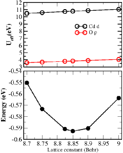
The lattice constants () and bulk moduli () for each of the II-VI semiconductors in the three bulk phases are obtained by fitting the total energy as a function of volume to the Murnaghan’s equation of state (eos). As discussed in Sec. II, is a functional of the electron density and is thus dependent on the geometry of the ground state. For a small volume change around equilibrium, the calculated varies linearly with the volume. As an example, In the top of Fig. 1 we have plotted the variation of for CdO in the rs phase where we observe the linear scaling for both the Cd’s and the O’s , most likely related to bond length changes that affect the wave-functions overlap and the electron localization.
| Phase | Zn3d | Anion p | |
|---|---|---|---|
| ZnO | wz | 13.19 | 5.57 |
| zb | 13.24 | 6.02 | |
| rs | 13.52 | 6.05 | |
| ZnS | wz | 13.48 | 3.50 |
| zb | 13.21 | 3.42 | |
| rs | 14.54 | 3.76 | |
| ZnSe | wz | 15.00 | 2.55 |
| zb | 14.60 | 2.52 | |
| rs | 15.68 | 2.77 | |
| ZnTe | wz | 16.00 | 2.40 |
| zb | 16.89 | 2.43 | |
| rs | 17.08 | 2.66 |
| Phase | Cd 4d | Anion p | |
|---|---|---|---|
| CdO | wz | 10.69 | 4.50 |
| zb | 10.49 | 4.03 | |
| rs | 10.73 | 3.92 | |
| CdS | wz | 11.07 | 3.69 |
| zb | 10.89 | 3.64 | |
| rs | 11.77 | 3.94 | |
| CdSe | wz | 11.58 | 2.68 |
| zb | 11.69 | 2.70 | |
| rs | 12.51 | 3.05 | |
| CdTe | wz | 12.95 | 2.57 |
| zb | 13.00 | 2.55 | |
| rs | 13.70 | 2.46 |
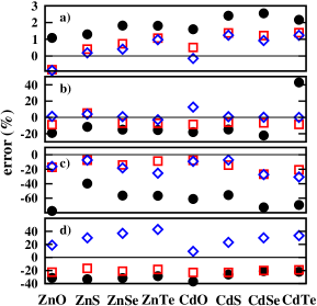
In Tables. 3 and 4, we have listed all the values of the computed lattice constants and bulk moduli of all the II-VI semiconductors in the three phases using PBE, HSE and ACBN0 (and SIRC, whenever available) with references to existing experimental values. Experimentally, the lattice constants follow the trend of ZnO ZnS ZnSe ZnTe and similarly for the CdX series. This trend of increasing lattice constant is described in the PBE, HSE and ACBN0 functionals. The experimental bulk moduli shows a reverse trend i.e., the bulk modulus decreases as we go from O to S to Se to Te.
In Figures 2(a) and 2(b), we have plotted the relative percentage error of the three functionals PBE, HSE, and ACBN0 in predicting the lattice constants and bulk moduli with respect to the measured values. In the plot, we have included only the stable phases for each of the eight semiconductors since we did not have experimental data on the non-equilibrium phases. The values for the other three phases for the II-VI semiconductors are listed in Table 3. Except for CdO and ZnO, all the other semiconductors have a stable zb structure. For ZnO, we have listed the error for one of the lattice parameters, , while for CdO we have used the rs phase.
The lattice constants and bulk modulii are more accurately described by HSE and ACBN0 compared to PBE functional calculations. The PBE overestimates the lattice constants significantly (up to 2%) as seen in Fig. 2(a) and severely underestimates the bulk-moduli (See Fig. 2(b)); in some cases the error is more than 50% compared to the experimental value. The HSE functional shows a better improvement in the prediction of lattice constants reducing the error to less than 1%. The lattice constants predicted by the ACBN0 follows the HSE closely with an error less than 1%. Note that the ACBN0 preserves the accuracy of the HSE calculations with 8-10 times speed up in terms of calculation time.
The bulk modulus predicted by ACBN0 shows a tremendous improvement over both the HSE and the PBE functional. In CdS, CdSe and CdTe, the agreement with experimental values is exceptional with an error less than (0.5%). Note that the PBE error in the bulk moduli are greater than 20%. These results indicates that using ACBN0 for the calculations of phonon spectra or any lattice dynamical property will yield much improved results, as already observed in the case of ZnO,Calzolari and Buongiorno Nardelli (2013) where the values of the Zn and O ’s, originally fitted to reproduce the experimental band gap and position of the d bands, are in remarkable agreement with the ones predicted by ACBN0. Incidentally, values fitted to HSE calculations have been proposed in the past for ZnO and ZnS.Andriotis et al. (2013); Hong et al. (2012) While for ZnO the values are again close to our predictions, the values for ZnS are very much different. See Sec. III.3 for a comprehensive discussion of the lattice dynamical properties of these systems.
For all other phases, the ACBN0 functional reproduces the HSE values closely as seen in Table 3 and 4 at a much lower computational cost. Overall the the structural properties of the II-VI semiconductors computed with the ACBN0 functional show better agreement with respect to experimental results.
. System Phase PBE HSE SIRC ACBN0 Experiment ZnO wz 3.283, 5.309 3.260, 5.221 3.290, 5.29 3.270, 5.164 3.258, 5.220 Springer Materials: The Landolt-Börnstein Database zb 4.670 4.582 4.580 4.620 Ashrafi and Jagadish (2007); Uddin and Scuseria (2006) rs 4.370 4.278 4.289 4.272 Uddin and Scuseria (2006); Fan et al. (2008) ZnS wz 3.880,6.300 3.850,6.271 3.830,6.280 3.851, 6.278 3.811, 6.234 Grünwald et al. (2012) zb 5.489 5.432 5.421 5.437 5.410 Springer Materials: The Landolt-Börnstein Database rs 5.143 5.077 5.080 5.060 Jaffe et al. (1993); Grünwald et al. (2012) ZnSe wz 4.043,6.70 4.030,6.620 4.020, 6.630 3.980,6.530 Springer Materials: The Landolt-Börnstein Database ; Vogel et al. (1996) zb 5.771 5.708 5.696 5.667 Springer Materials: The Landolt-Börnstein Database ; Heyd et al. (2005) rs 5.401 5.330 5.321 ZnTe wz 4.366,7.176 4.35,7.132 4.340, 7.140 4.320,7.100 Lakshmi et al. (2003) zb 6.199 6.154 6.148 6.089 Vogel et al. (1996); Heyd et al. (2005) rs 5.788 5.743 5.732 CdO wz 3.700,5.850 3.650,5.800 3.590,5.750 zb 5.172 5.103 5.054 rs 4.771 4.722 4.781 4.689 4.696 Schleife et al. (2006); Burbano et al. (2011); Mudd et al. (2014) CdS wz 4.206,6.85 4.223,6.951 4.154,6.762 4.183,6.682 4.135,6.701 Shi et al. (2014); Grünwald et al. (2012) zb 5.963 5.901 5.851 5.892 5.820 Hinuma et al. (2013); Springer Materials: The Landolt-Börnstein Database ; Grünwald et al. (2012) rs 5.890 5.466 5.459 CdSe wz 4.39,7.1 4.350,7.112 4.292,7.021 4.33,7.072 4.310,7.010 Vogel et al. (1996) zb 6.239 6.158 6.071 6.142 6.084 Vogel et al. (1996) rs 5.800 5.697 5.680 CdTe wz 4.550, 7.451 4.580,7.460 4.600, 7.498 zb 6.621 6.571 6.401 6.560 6.480 Heyd et al. (2005) rs 6.130 6.092 6.076
| System | Phase | PBE | HSE | SIRC | ACBN0 | Experiment |
|---|---|---|---|---|---|---|
| ZnO | wz | 127 | 143 | 159 | 157 | 136-183 Uddin and Scuseria (2006); Springer Materials: The Landolt-Börnstein Database ; Vogel et al. (1996) |
| zb | 123 | 143 | 162 | |||
| rs | 156 | 188 | 205 | 177-228 Uddin and Scuseria (2006) | ||
| ZnS | wz | 60 | 74 | 81 | 79 | 76 Kisi and Elcombe (1989) |
| zb | 68 | 74.4 | 81 | 80 | 76.9 Springer Materials: The Landolt-Börnstein Database | |
| rs | 84 | 95.4 | 101.6 | 103.6 Jaffe et al. (1993) | ||
| ZnSe | wz | 57 | 62.69 | 64 | ||
| zb | 55.8 | 61 | 66.3 | 65.7 Heyd et al. (2005) | ||
| rs | 70 | 78 | 66.8 | |||
| ZnTe | wz | 45 | 58.46 | 56 | ||
| zb | 43 | 47.19 | 49.4 | 50.9 Vogel et al. (1996); Heyd et al. (2005) | ||
| rs | 53.3 | 58.82 | 60 | |||
| CdO | wz | 92.7 | 104 | 114 | ||
| zb | 91 | 102 | 124 | |||
| rs | 119 | 137 | 152 | 170 | 147 Liu et al. (2006) | |
| CdS | wz | 54 | 57 | 74 | 53 | 61 Vogel et al. (1996), 65 Grünwald et al. (2012) |
| zb | 53.5 | 58.94 | 70 | 63.3 | 55 Grünwald et al. (2012) | |
| rs | 63.3 | 78.6 | 83.2 | |||
| CdSe | wz | 48 | 50.80 | 62 | 52 | 55 |
| zb | 41.5 | 49.7 | 66 | 53.4 | 45.1 Grünwald et al. (2012) | |
| rs | 53 | 67.4 | 64 | |||
| CdTe | wz | 55 | 60 | 57.4 | ||
| zb | 57 | 38.4 | 52 | 42 | 42 Springer Materials: The Landolt-Börnstein Database | |
| rs | 45 | 51.86 | 53.1 |
III.2 Electronic properties
The band-structures of the eight semiconductors in all the three different crystal phases were computed to assess the veracity of the ACBN0 functional in the prediction of band gaps. For comparison, we computed the band-structures within the PBE and the HSE functionals. All the band structures were calculated at the theoretical equilibrium volume optimized within each functional. In the wz and zb compounds, the band-gap is direct while in the rs compounds the gap is indirect between the and point. A summary of the values of the energy-gaps () for the different compounds is presented in Table 5 as calculated by the ACBN0, PBE and HSE functionals along with references to the SIRC and experimental values whenever available.
| System | Phase | PBE | HSE | SIRC | ACBN0 | Experiment |
|---|---|---|---|---|---|---|
| ZnO | wz | 0.85 | 2.90 | 3.4 | 2.91 | 3.2 Springer Materials: The Landolt-Börnstein Database , 3.4 Uddin and Scuseria (2006) |
| zb | 0.59 | 2.70 | 2.74 | 3.27 Ashrafi and Jagadish (2007) | ||
| rs | 2.17 (0.89) | 4.35(2.90) | 4.17(3.09) | 4.5(2.45) Kuang et al. (2014) | ||
| ZnS | wz | 2.10 | 3.42, 3.34 Yadav and Ramprasad (2012) | 3.6 | 3.31 | 3.86 Kisi and Elcombe (1989), 3.91 Kasap and Capper (2007) |
| zb | 2.23 | 3.49 Peverati and Truhlar (2012) | 3.6 | 3.42 | 3.7 Springer and Aryasetiawan (1998), 3.66 Heyd et al. (2005) | |
| rs | 2.1(0.83) | 3.7(1.31) | 3.52(1.28) | |||
| ZnSe | wz | 1.27 | 2.46 | 1.90 | 2.87 | |
| zb | 1.18 | 2.32 Heyd et al. (2005),2.42 Peverati and Truhlar (2012) | 2.1 | 2.041 | 2.70 Heyd et al. (2005) | |
| rs | 1.4(0) | 2.60(0) | 2.02(0) | |||
| ZnTe | wz | 1.17 | 2.22 | 1.82 | ||
| zb | 1.043 | 2.36 Peverati and Truhlar (2012),2.19 Heyd et al. (2005) | 1.4 | 1.79 | 2.38 Heyd et al. (2005) | |
| rs | 0.6 | 1.4 | 1.2 | |||
| CdO | wz | 0 | 0.75, 1.13 Yan et al. (2012) | 1.23 | 0.91 Janotti et al. (2006) | |
| zb | 1.04 | 1.35 | ||||
| rs | 0.85() | 2.01(0.89) | 1.98(0.70) | 2.18-2.23(0.9-1.08) Mudd et al. (2014); Vasheghani Farahani et al. (2013) | ||
| CdS | wz | 1.36 | 2.15, 2.09 Shi et al. (2014) | 2.5 | 2.4 | 2.5 Rossow et al. (1993) |
| zb | 1.11 | 2.13 | 2.4 | 2.3 | 2.55 Heyd et al. (2005), 2.4 Vogel et al. (1996) | |
| rs | 1.71(0) | 2.9(1.4) | 2.95(1.27) | 1.5 Heyd et al. (2005) | ||
| CdSe | wz | 0.73 | 1.77 | 1.3 | 1.61 | 1.8 Vogel et al. (1996) |
| zb | 0.52 | 1.39 | 1.4 | 1.38 | 1.90 Heyd et al. (2005),1.82 Vogel et al. (1996) | |
| rs | 0 | 0.69(0) | 1.4(0.3) | |||
| CdTe | wz | 0.64 | 1.6 | 1.33 | 1.8 | |
| zb | 0.58 | 1.51, 1.52 Xiao et al. (2011),1.67 Peverati and Truhlar (2012) | 0.8 | 1.43 | 1.92 Heyd et al. (2005),1.61 Xiao et al. (2011) | |
| rs | (0) | 1.4(0) | 1.3(0) |
Experimentally, the band gap in both the ZnX and the CdX series decreases with increasing lattice constants i.e., the band gap decreases as we proceed from S to Se to Te. Both ZnO and CdO show the anomaly of a lower band-gap compared to the ZnS and CdS respectively, in spite of a lower lattice constant. This trend of decreasing band gap is described by all the functionals: PBE, HSE and ACBN0. The absolute value of the band-gap, however, is severely underestimated by PBE: in the oxides, especially, we see an error bar of more than 60% (See Fig.2 (c)). The ACBN0 functional reduces this error to less than 20%. The band-gaps predicted by ACBN0 for the eight semiconductors studied here lie within 0.5 eV of the experimental value.
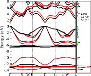
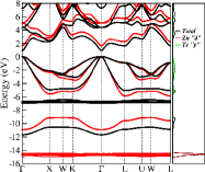
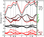
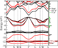
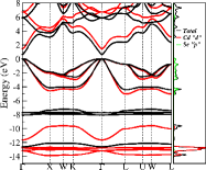
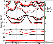
Before discussing the similarities of the HSE and the ACBN0 functionals, we first look at the general features of the calculated band-structures. Representative band-structures for the eight semiconductors in their stable phases calculated with the ACBN0 and the PBE functional are shown in Figures 3 and 4 (band structure of all the other phases are compiled in the Supplementary Information). Within PBE, (black lines), the overall band profiles are very similar in both the ZnX and CdX series. The lowest energy manifolds (below -10 eV) are rather narrow and entirely of s character. At higher energy we found the bands derived from the d orbitals of Zn and Cd that are just below (or little hybridized) with the oxygen and chalcogen p states forming the manifolds at the top of the valence band. The conduction band is dominated by the cation s states. As we proceed from S to Te, the chalcogen p states shift up in energy and this results in the disentangling of the d bands. Compared to ZnS, in CdS the Cd d bands are already well-separated from the S p bands. As seen from the PBE band-structures, in both ZnO and CdO the d states are more dispersed compared to the chalcogenides. The presence of a spurious p-d hybridization in ZnO is a macroscopic manifestation of the inadequacy of traditional (semi)local functionals to predict correctly the electronic properties of materials where strong electron localization is present and results in the strong underestimation of the band-gap: 0.85 eV versus an experimental value of 3.4 eV. Finally, CdO is predicted to be a semi-metal by PBE. As it is clearly evident from the figures, the ACBN0 bands (red lines) maintain their overall character as discussed above but display a much wider separation between valence and conduction bands. The relative position of the d bands is shifted to lower energies, thus promoting the disentanglement of the Zn and O manifolds. For instance, the ACBN0 converged values for ZnO and CdO energy gaps are 2.91 eV and 0.70 eV, respectively, in better agreement with the experimental values of 3.4 eV and 0.9 eV. At the same time, the Zn bands of ZnO are shifted by approximately 4 eV with respect to the O bands, removing the spurious hybridization present in PBE.
Note that the ACBN0 follows the HSE functional in predicting the band-gaps. Both the ACBN0 and the hybrid functionals reduce the static correlation energy associated with the localized orbitals and hence provide a similar correction. Indeed, Ivady et.al (Ref. Ivády et al., 2014) have recently shown that the hybrid exchange correlation potential can be rewritten mathematically as an on-site Hubbard potential for a system of localized orbitals, thus providing a formal justification for our observations.
| Compound | PBE | HSE | ACBN0 | Experiment |
|---|---|---|---|---|
| ZnO | -5.5 | -6.2 | -9.3 | -7.8 |
| ZnS | -6.0 | -7.5 | -11.7 | -9.0 |
| ZnSe | -6.5 | -7.5 | -12.9 | -9.4 |
| ZnTe | -7.0 | -8.0 | -13.8 | -9.8 |
| CdO | -5.5 | -6.8 | -9.5 | -8.7 |
| CdS | -7.0 | -7.4 | -12.0 | -9.6 |
| CdSe | -7.8 | -8.0 | -13.0 | -10.0 |
| CdTe | -8.3 | -8.4 | -14.0 | -10.5 |
In Fig. 2(d) we have plotted the error bar in the position of the manifold of Zn and Cd in PBE, HSE and ACBN0. We clearly observe the limits of ACBN0 and HSE in predicting the energy of the d bands relative to the valence band maximum. In PBE and HSE, we see a negative error of around 40% which indicates that the position of the d bands are higher in energy compared to the experimental values while in ACBN0, the bands are pushed much lower, closer to the experimental position. The reason for the overestimation of the d band energy in HSE calculations is due to the incomplete treatment of correlation energy of the localized d electrons. In ACBN0, downward shifting of the 3 or 4 bands increase monotonically with increasing values of . The rigid shift of the bands arises from a singularity due to the filled character of the bands and it is implicit in the definition of the Hubbard correction. An extensive discussion for the case of ZnO is provided in Ref. Agapito et al., 2015.
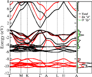 |
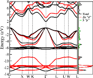 |
 |
 |
| ZnO | ZnS | ZnSe | ZnTe |
 |
 |
 |
 |
| CdO | CdS | CdSe | CdTe |
III.3 Lattice dynamical properties
In the wide band gap semiconductors, the incorrect description of the covalency of the cation-anion bond affects the electrostatic properties of the system and, consequently, the phonon distribution and the coupling with the external fields. This problem is more pronounced in the oxides compared to the chalcogenides. In ZnO the underestimated band-gap within PBE functionals leads to an overestimate of the high-frequency dielectric constant () and, in turn, a large discrepancy in the LO-TO splitting. The PBE value of 5.24 is higher compared to the experimental value of 3.14 (Ref. Calzolari and Buongiorno Nardelli, 2013). Similarly, in CdO the PBE dielectric constant is 7.13 compared to the experimental value of 5.3. This trend of overestimation of the high-frequency dielectric constant is observed in the other chalcogenides as well.
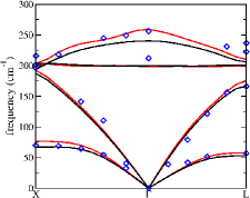
The ACBN0 functional provides a proper description of the electronic and structural features of the II-VI semiconductors and improves the dielectric and vibrational properties leading, in most cases, to smaller deviations with respect to the experimental data. The calculated high frequency dielectric constants (), the Born effective charges () and the zone-center phonon frequencies are summarized in Tables 8 and 7. We did not find any references to vibrational properties calculated within the HSE method which is computationally very expensive especially for calculating the response functions.
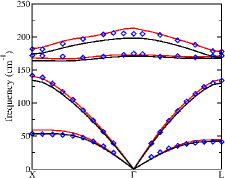
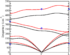
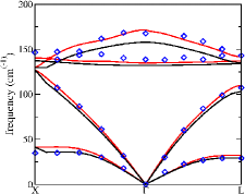
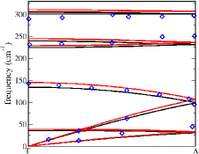
In this section we also show the accuracy of the phonon spectrum for six representative compounds: ZnS, ZnSe, ZnTe, CdO, CdS, and CdTe. ACBN0 phonons frequencies are compared with the PBE and experimental values. The dielectric properties and the vibrational spectrum of the II-VI semiconductors were calculated using a coupled finite-fields/finite differences approach as discussed extensively in Ref. Calzolari and Buongiorno Nardelli, 2013. The PBE and ACBN0 phonon dispersions are reported in Figures 5 and 6. In the Zn chalcogenides the acoustic manifold is equally well reproduced within the PBE and the ACBN0 formalisms (deviations of few cm-1 with respect to the available experimental data). For the optic manifold, however, ACBN0 improves the agreement with experiment. This result may be rationalized in terms of the more accurate description of the bonding. In both CdO and CdTe, the ACBN0 values are in excellent agreement with the experiments and improve the PBE description especially for the optic manifolds. In CdS both ACBN0 and PBE are in good agreement with the experiments.
 |
 |
 |
| ZnS | ZnSe | ZnTe |
 |
 |
 |
| CdO | CdTe | CdS |
| System | Mode | PBE | ACBN0 | Experiment |
|---|---|---|---|---|
| ZnS | TO() | 259 | 266 | 273 |
| LO() | 329 | 364 | 344 | |
| TO(X) | 293 | 301 | 312 | |
| LO(X) | 309 | 327 | 326 | |
| TO(L) | 273 | 280 | 286 | |
| LO(L) | 319 | 337 | 333 | |
| ZnSe | TO() | 199 | 198 | 213 |
| LO() | 240 | 260 | 254 | |
| TO(X) | 204 | 203 | 216 | |
| LO(X) | 204 | 203 | 225 | |
| TO(L) | 201 | 200 | 222 | |
| LO(L) | 205 | 210 | 236 | |
| ZnTe | TO() | 170 | 172 | 175 |
| LO() | 198 | 213 | 204 | |
| TO(X) | 164 | 168 | 183 | |
| LO(X) | 174 | 182 | 181 | |
| TO(L) | 167 | 170 | 171 | |
| LO(L) | 168 | 177 | 177 | |
| CdO | TO() | 234 | 251 | 266 |
| LO() | 410 | 462 | 465 | |
| TO(X) | 290 | 325 | 331 | |
| CdTe | TO() | 132 | 134 | 138 |
| LO() | 158 | 171 | 167 | |
| TO(X) | 137 | 140 | ||
| LO(X) | 137 | 140 | 147 | |
| TO(L) | 133 | 137 | ||
| LO(L) | 134 | 141 | 142 |
| Z | ||||||
|---|---|---|---|---|---|---|
| System | PBE | ACBN0 | Experiment | PBE | ACBN0 | Experiment |
| ZnS | 5.98 | 4.12 | 5.13 | 2.02 | 2.10 | 2.1 |
| ZnSe | 7.40 | 4.98 | 5.70 | 2.12 | 2.17 | 2.21 |
| ZnTe | 9.38 | 6.01 | 7.2 | 2.22 | 2.19 | 2.0 |
| CdO | 7.13 | 3.52 | 5.3 | 2.40 | 1.97 | |
| CdTe | 9.13 | 5.56 | 7.1 | 2.45 | 2.34 | 2.06 |
IV Conclusions
The procedure to compute from first principles the Hubbard correction as implemented in the ACBN0 functional largely improves the electronic structure with respect to PBE. The energy band gap in Cd and Zn oxides and chalcogenides computed within the ACBN0 formalism is very close to the value computed with hybrid functional at a computational cost of roughly 10%. The ACBN0 functional generally improves the structural and the vibrational parameters reaching improved agreement with the experiments. Both hybrid functionals and ACBN0 have limited predictive value when considering the the position of the occupied d manifolds, at least in ZnS, ZnSe, ZnTe, ZnO, CdS, CdSe, CdTe, and CdO that we investigated.
Acknowledgements.
We thank A. Calzolari, H. Shi, I. Takeuchi, G. Hart and R. Forcade for various technical discussions that have contributed to the results reported in this article. This work was supported by ONR-MURI under contract N00014-13-1-0635, DOD-ONR (N00014-14-1-0526) and the Duke University Center for Materials Genomics. S.C. acknowledges partial support by DOE (DE-AC02-05CH11231, BES program under Grant #EDCBEE). We also acknowledge the Texas Advanced Computing Center (TACC) at the University of Texas Austin for providing HPC resources, and the CRAY corporation for computational assistance.References
- Wang and Isshiki (2007) J. Wang and M. Isshiki, in Springer Handbook of Electronic and Photonic Materials, edited by S. Kasap and P. Capper (Springer US, 2007) pp. 325–342.
- Perdew and Zunger (1981a) J. P. Perdew and A. Zunger, Phys. Rev. B 23, 5048 (1981a).
- Perdew et al. (1996) J. P. Perdew, K. Burke, and M. Ernzerhof, Phys. Rev. Lett. 77, 3865 (1996).
- Mang et al. (1995) A. Mang, K. Reimann, and S. Rübenacke, Solid State Commun. 94, 251 (1995).
- Powell et al. (1972) R. A. Powell, W. E. Spicer, and J. C. McMenamin, Phys. Rev. B 6, 3056 (1972).
- Schleife et al. (2006) A. Schleife, F. Fuchs, J. Furthmüller, and F. Bechstedt, Phys. Rev. B 73, 245212 (2006).
- Demchenko et al. (2010) I. N. Demchenko, J. D. Denlinger, M. Chernyshova, K. M. Yu, D. T. Speaks, P. Olalde-Velasco, O. Hemmers, W. Walukiewicz, A. Derkachova, and K. Lawniczak-Jablonska, Phys. Rev. B 82, 075107 (2010).
- Vogel et al. (1996) D. Vogel, P. Krüger, and J. Pollmann, Phys. Rev. B 54, 5495 (1996).
- Ley et al. (1974) L. Ley, R. A. Pollak, F. R. McFeely, S. P. Kowalczyk, and D. A. D. A. Shirley, Phys. Rev. B 9, 600 (1974).
- Perdew and Zunger (1981b) J. P. Perdew and A. Zunger, Phys. Rev. B 23, 5048 (1981b).
- Perdew and Levy (1983) J. P. Perdew and M. Levy, Phys. Rev. Lett. 51, 1884 (1983).
- Sham and Schluter (1983) L. J. Sham and M. Schluter, Phys. Rev. Lett. 51, 1888 (1983).
- Perdew et al. (1982) J. P. Perdew, R. B. Parr, M. Levy, and J. L. Balduz, Phys. Rev. Lett. 49, 1691 (1982).
- Anisimov et al. (1997) V. I. Anisimov, F. Aryasetiawan, and A. I. Lichtenstein, J. Phys.: Conden. Matt. 9, 767 (1997).
- Liechtenstein et al. (1995) A. I. Liechtenstein, V. I. Anisimov, and J. Zaanen, Phys. Rev. B 52, R5467 (1995).
- Aryasetiawan and Gunnarsson (1998) F. Aryasetiawan and O. Gunnarsson, Rep. Prog. Phys. 61, 237 (1998).
- Fuchs et al. (2007) F. Fuchs, J. Furthmüller, F. Bechstedt, M. Shishkin, and G. Kresse, Phys. Rev. B 76, 115109 (2007).
- Shishkin and Kresse (2007) M. Shishkin and G. Kresse, Phys. Rev. B 75, 235102 (2007).
- Heyd et al. (2003a) J. Heyd, G. E. Scuseria, and M. Ernzerhof, J. Chem. Phys. 118, 8207 (2003a).
- Heyd et al. (2006) J. Heyd, G. E. Scuseria, and M. Ernzerhof, J. Phys. Chem. 124, 219906 (2006).
- Himmetoglu et al. (2014) B. Himmetoglu, A. Floris, S. de Gironcoli, and M. Cococcioni, International Journal of Quantum Chemistry 114, 14 (2014).
- Springer and Aryasetiawan (1998) M. Springer and F. Aryasetiawan, Phys. Rev. B 57, 4364 (1998).
- Gunnarsson et al. (1989) O. Gunnarsson, O. K. Andersen, O. Jepsen, and J. Zaanen, Phys. Rev. B 39, 1708 (1989).
- Cococcioni and de Gironcoli (2005) M. Cococcioni and S. de Gironcoli, Phys. Rev. B 71, 035105 (2005).
- Kümmel and Kronik (2008) S. Kümmel and L. Kronik, Rev. Mod. Phys. 80, 3 (2008).
- Editorial (2013) Editorial, Nat. Mater. 12, 173 (2013).
- Agapito et al. (2013) L. A. Agapito, A. Ferretti, A. Calzolari, S. Curtarolo, and M. Buongiorno Nardelli, Phys. Rev. B 88, 165127 (2013).
- Curtarolo et al. (2013) S. Curtarolo, G. L. W. Hart, M. Buongiorno Nardelli, N. Mingo, S. Sanvito, and O. Levy, Nat. Mater. 12, 191 (2013).
- Taylor et al. (2014) R. H. Taylor, F. Rose, C. Toher, O. Levy, K. Yang, M. Buongiorno Nardelli, and S. Curtarolo, Comp. Mat. Sci. 93, 178 (2014).
- Agapito et al. (2015) L. A. Agapito, S. Curtarolo, and M. Buongiorno Nardelli, Phys. Rev. X 5, 011006 (2015).
- Dudarev et al. (1998) S. L. Dudarev, G. A. Botton, S. Y. Savrasov, C. J. Humphreys, and A. P. Sutton, Phys. Rev. B 57, 1505 (1998).
- Andriotis et al. (2013) A. N. Andriotis, G. Mpourmpakis, S. Lisenkov, R. M. Sheetz, and M. Menon, physica status solidi (b) 250, 356 (2013).
- Giannozzi et al. (2009) P. Giannozzi, S. Baroni, N. Bonini, M. Calandra, R. Car, C. Cavazzoni, D. Ceresoli, G. L. Chiarotti, M. Cococcioni, I. Dabo, A. Dal Corso, S. de Gironcoli, S. Fabris, G. Fratesi, R. Gebauer, U. Gerstmann, C. Gougoussis, A. Kokalj, M. Lazzeri, L. Martin-Samos, N. Marzari, F. Mauri, R. Mazzarello, S. Paolini, A. Pasquarello, L. Paulatto, C. Sbraccia, S. Scandolo, G. Sclauzero, A. P. Seitsonen, A. Smogunov, P. Umari, and R. M. Wentzcovitch, J. Phys.: Conden. Matt. 21, 395502 (2009).
- Calzolari et al. (2004) A. Calzolari, N. Marzari, I. Souza, and M. Buongiorno Nardelli, Phys. Rev. B 69, 035108 (2004).
- (35) See, for instance, WanT code by A. Ferretti, B. Bonferroni, A. Calzolari, and M. Buongiorno Nardelli, (http://www.wannier-transport.org).
- Kresse and Furthmüller (1996) G. Kresse and J. Furthmüller, Phys. Rev. B 54, 11169 (1996).
- Heyd et al. (2003b) J. Heyd, G. E. Scuseria, and M. Ernzerhof, J. Chem. Phys. 118, 8207 (2003b).
- Calzolari and Buongiorno Nardelli (2013) A. Calzolari and M. Buongiorno Nardelli, Sci. Rep. 3 (2013), 10.1038/srep02999.
- Hong et al. (2012) J. Hong, A. Stroppa, J. Íñiguez, S. Picozzi, and D. Vanderbilt, Physical Review B 85, 054417 (2012).
- (40) Springer Materials: The Landolt-Börnstein Database, “http://www.springermaterials.com/docs/index.html,” .
- Ashrafi and Jagadish (2007) A. Ashrafi and C. Jagadish, Journal of Applied Physics 102, 071101 (2007).
- Uddin and Scuseria (2006) J. Uddin and G. E. Scuseria, Phys. Rev. B 74, 245115 (2006).
- Fan et al. (2008) C. Fan, Q. Wang, L. Li, S. Zhang, Y. Zhu, X. Zhang, M. Ma, R. Liu, and W. Wang, Applied Physics Letters 92, 101917 (2008).
- Grünwald et al. (2012) M. Grünwald, A. Zayak, J. B. Neaton, P. L. Geissler, and E. Rabani, The Journal of chemical physics 136, 234111 (2012).
- Jaffe et al. (1993) J. Jaffe, R. Pandey, and M. Seel, Physical Review B 47, 6299 (1993).
- Heyd et al. (2005) J. Heyd, J. E. Peralta, G. E. Scuseria, and R. L. Martin, The Journal of chemical physics 123, 174101 (2005).
- Lakshmi et al. (2003) N. Lakshmi, N. M. Rao, R. Venugopal, D. Reddy, and B. Reddy, Materials Chemistry and Physics 82, 764 (2003).
- Burbano et al. (2011) M. Burbano, D. O. Scanlon, and G. W. Watson, Journal of the American Chemical Society 133, 15065 (2011).
- Mudd et al. (2014) J. J. Mudd, T.-L. Lee, V. Muñoz Sanjosé, J. Zúñiga Pérez, D. J. Payne, R. G. Egdell, and C. F. McConville, Phys. Rev. B 89, 165305 (2014).
- Shi et al. (2014) L. Shi, Y. Qin, J. Hu, Y. Duan, L. Qu, L. Wu, and G. Tang, EPL (Europhysics Letters) 106, 57001 (2014).
- Hinuma et al. (2013) Y. Hinuma, F. Oba, Y. Kumagai, and I. Tanaka, Phys. Rev. B 88, 035305 (2013).
- Kisi and Elcombe (1989) E. H. Kisi and M. M. Elcombe, Acta Crystallographica Section C: Crystal Structure Communications 45, 1867 (1989).
- Liu et al. (2006) H. Liu, J. S. Tse, and H.-k. Mao, Journal of applied physics 100, 093509 (2006).
- Kuang et al. (2014) F.-G. Kuang, X.-Y. Kuang, S.-Y. Kang, M.-M. Zhong, and A.-J. Mao, Materials Science in Semiconductor Processing 23, 63 (2014).
- Yadav and Ramprasad (2012) S. Yadav and R. Ramprasad, Applied Physics Letters 100, 241903 (2012).
- Kasap and Capper (2007) S. Kasap and P. Capper, Springer handbook of electronic and photonic materials (Springer, 2007).
- Peverati and Truhlar (2012) R. Peverati and D. G. Truhlar, The Journal of chemical physics 136, 134704 (2012).
- Yan et al. (2012) Q. Yan, P. Rinke, M. Winkelnkemper, A. Qteish, D. Bimberg, M. Scheffler, and C. G. Van de Walle, Applied Physics Letters 101, 152105 (2012).
- Janotti et al. (2006) A. Janotti, D. Segev, and C. G. V. de Walle, Phys. Rev. B 74, 045202 (2006).
- Vasheghani Farahani et al. (2013) S. K. Vasheghani Farahani, V. Muñoz-Sanjosé, J. Zúñiga-Pérez, C. F. McConville, and T. D. Veal, Applied Physics Letters 102, 022102 (2013).
- Rossow et al. (1993) U. Rossow, T. Werninghaus, D. Zahn, W. Richter, and K. Horn, Thin solid films 233, 176 (1993).
- Xiao et al. (2011) H. Xiao, J. Tahir-Kheli, and W. A. Goddard III, The Journal of Physical Chemistry Letters 2, 212 (2011).
- Ivády et al. (2014) V. Ivády, R. Armiento, K. Szász, E. Janzén, A. Gali, and I. A. Abrikosov, Phys. Rev. B 90, 035146 (2014).
- Setyawan and Curtarolo (2010) W. Setyawan and S. Curtarolo, Comp. Mat. Sci. 49, 299 (2010).
- Hennion et al. (1971) B. Hennion, F. Moussa, G. Pepy, and K. Kunc, Physics Letters A 36, 376 (1971).
- Vagelatos et al. (1974) N. Vagelatos, D. Wehe, and J. King, The Journal of Chemical Physics 60, 3613 (1974).
- Oliva et al. (2013) R. Oliva, J. Ibáñez, L. Artús, R. Cuscó, J. Zúñiga-Pérez, and V. Muñoz-Sanjosé, Journal of Applied Physics 113, 053514 (2013).
- Rowe et al. (1974) J. Rowe, R. Nicklow, D. Price, and K. Zanio, Physical Review B 10, 671 (1974).