Optical signatures of states bound to vacancy defects in monolayer MoS2
Abstract
We show that pristine MoS2 single layer (SL) exhibits two bandgaps eV and eV for the optical in-plane and out-of-plane susceptibilities and , respectively. In particular, we show that odd states bound to vacancy defects (VDs) lead to resonances in inside in MoS2 SL with VDs. We use density functional theory, the tight-binding model, and the Dirac equation to study MoS2 SL with three types of VDs: (i) Mo-vacancy, (ii) S2-vacancy, and (iii) 3MoS2 quantum antidot. The resulting optical spectra identify and characterize the VDs.
pacs:
61.72.jd,42.65.An,71.15.-m,73.22.-fIntroduction.
Monolayer transition metal dichalcogenides (TMDCs) (MX2; M= transition metal such as Mo, W and X=S, Se, Te) have attracted a lot of attention due to their intriguing electronic properties. Monolayer TMDCs are semiconductors with direct bandgap in the visible range, which makes them suitable for optoelectronic, spintronic, valleytronic, and photodetector devices Splendiani et al. (2010); Mak et al. (2010); Zhu et al. (2011); Xiao et al. (2012); Lopez-Sanchez et al. (2013); Liu et al. (2013); Rostami et al. (2013). In order to increase the performance of such devices based on TMDC single layer (SL), it is crucial to characterize the defects present in TMDC SLs.
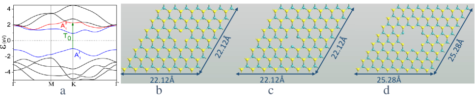
Here we show that the bandgap eV for the optical out-of-plane susceptibility in pristine MoS2 SL provides a large energy window to characterize vacancy defects (VDs). Pristine MoS2 SL is invariant with respect to reflection about the (Mo) plane, where the axis is oriented perpendicular to the Mo plane. Therefore, electron states break down into two classes: even and odd, or symmetric and anti-symmetric with respect to . We show below that this leads to the nontrivial consequence that has a bandgap of eV, which is substantially larger than the bandgap eV for the in-plane component of the optical susceptibility . As we show, due to the optical selection rules for the even and odd states, there are no transitions, driven by -polarized photons, below eV. Hence, for pristine MoS2 SL must vanish for energies below eV.
Several studies on VDs in 2D materials have emerged. The minibands resulting from quantum antidot (QAD) superlattices can be used to tune the bandgaps of graphene Pedersen et al. (2008) and MoS2 SL Huang et al. (2013); Shao et al. (2014). In another study, we have shown that substitutional defects in the form of MoO3 not only lead to strong suppression of the conductivity Islam et al. (2014) but also to photoluminescence quenching Kang et al. (2014). Recently, VDs in MoS2 SL have been characterized theoretically in terms of magnetic properties Zhou et al. (2013). A recent experimental study used scanning transmission electron spectroscopy to characterize several types of defects in MoS2 SL, including Mo, S, and S2 VDs Hong et al. (2015). MoS2 SL with S-vacancies might catalyze alcohol synthesis from syngas Le et al. (2014).
Here we show that VDs yield strong resonances in , which provides the opportunity to optically characterize VDs in MoS2 SL with VDs (denoted by MoS2 SLVD). We consider the optical signatures of states bound to three types of VDs in MoS2 SLVD: (i) Mo-vacancy, (ii) S2-vacancy, and (iii) a hexagonal 3MoS2 QAD (see Fig. 1).
Bandstructure.
First we start with the numerical bandstructure calculation of MoS2 SLVD using standard Density Functional Theory (DFT) with meta-GGA functionals Tao et al. (2003), providing accurate estimates of bandgaps without the need to perform computationally intensive DFT calculations using the GW approximation Faleev et al. (2004); Shishkin et al. (2007). The calculations are implemented within Atomistix Toolkit 2014.2 QW_ . The resulting bandstructures are shown in Fig. 2. The periodic structure of the superlattice allows one to characterize the electron states by the bandstructure , where is the vector in the first Brillouin zone of the superlattice and enumerates different bands. We consider supercells with dimensions (Fig. 2 b, c) and (Fig. 2 d) having and number of atoms, respectively. For Brillouin zone integration we consider sampling of . The cut off energy is set to eV and the structure is optimized by using a force convergence of eV/Å.
Tight-binding model (TBM) and symmetries.
Within the TBM approximation the electron wavefunction can be presented as , where enumerates atoms in the layer and the summation over runs over respective atomic orbitals, whose set for the -th atom is denoted . Choosing in the plane of the layer and perpendicularly, for Mo the real orbitals of main importance are the -orbitals , and so on, while for S atoms these are -orbitals with and and denoting the top and bottom layers, respectively. The classification of the electron states simplifies when the symmetry with respect to is taken into account. The electron states transform according to and , the irreducible representations of . The respective even and odd orbitals are locally spanned by the bases Cappelluti et al. (2013): and .
The full group of the point symmetries of MoS2 SLVD with our considered VDs is . Thus the states bound to the VDs, even and odd with respect to , must transform according to and , the irreducible representations of . Respectively, the bound states must appear as singlets and doublets. It should be noted that such classification holds if the overlap between states bound to different VDs is absent.
The simplest model describing the arrangement of the bound states is the TBM considering only the atoms on the edge of the VD, which is inferred by the small localization radius of the bound states. For the case of the hexagonal MoS2 QAD one finds
| (1) |
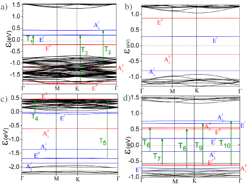
where , and for singlet states (invariant with respect to rotations) and for doublets (states aquiring the phase factor ). Here , are the phenomenological parameters describing the energy of the electron on Mo and S atoms, respectively, and is the hopping parameter. Equation (1) correctly reproduces the sequence for even and for odd states, i.e. singlet, doublet, doublet, singlet, while traversing the gap from the bottom of the conduction band down over the bound states (see Fig. 2d).
It may appear that this model contradicts the numerical results for the Mo-vacancy, where the numerical calculations show only bound states (see Fig. 2a). However, the TBM model suggests that in addition to the bound states appearing inside the gap of MoS2 SL there must be states, in this particular case a singlet state, hidden inside the bands. Indeed, there is such a state inside the valence band at energy eV below the top of the valence band (see Fig. 3b).
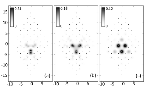
Moreover, the parameters and are determined by the microscopic Hamiltonian, e.g. . Thus, we can expect that there is a variety of states bound to VDs besides the ones inside the gaps , . An example of such states is provided by the case when the bound state is made of Sulfur’s -orbitals (see Fig. 3c) at energy eV below the Fermi level.
Dirac model.
The TBM considered above relates the structure of the spectrum of the bound states to the symmetry of the VD. Due to the fact that its parameters should be fitted to the energies of electron states obtained by other means, however, it cannot explain neither the smallness of the localization radius of the bound states nor their energies. In particular, it cannot explain why the odd states may form bound states inside the gap . These features, however, can be understood with the help of an analysis of circularly symmetric QADs based on the Dirac equation which emerges as the two-band model within the -approximation near the -point of the Brillouin zone of MoS2 SL.
Considering two bands with the energy separation between them, the equation describing the spatial distribution of the pseudo-spin has the form , where enumerates the valleys, the energy reference level is chosen to be positioned at the center between the bands, and . Assuming that the QAD has circular shape, we rewrite this equation in the polar coordinates and with respect to we obtain , where
| (2) |
The solution is subject to the condition of vanishing radial component of the probability current at the boundary McCann and Fal’ko (2004); Akhmerov and Beenakker (2008) , where is the radius of the QAD and is the unit vector perpendicular to the boundary. The straightforward implementation of such boundary condition is provided by the infinite mass model Berry and Mondragon (1987), where the QAD is represented by a region with renormalized width of the gap , with for and when . In our case we identify . Within this model the boundary condition is satisfied if , i.e. the pseudo-spin is tangent to the boundary of the QAD. Next, observing that and , one can see that has an angularly independent solution corresponding to , which exponentially decays for with the localization radius .
Thus, independently of its radius the QAD may support a bound state with very short localization length and with the energy in the middle between the energies of the coupled bands. Comparing this finding to the distribution of energies of even and odd bands Cappelluti et al. (2013) the conclusion can be drawn that, indeed, both even and odd bands may support bound states with the energy near the energy of the Fermi level, i.e. inside the gap of MoS2 SL.
Optical spectrum.
In view of nontriviality of the appearance of odd bond states inside the gap it is important to note that the presence of the bound states of different parities manifests itself in the optical spectrum of MoS2 SLVD. Therefore, they are available for a direct experimental observation.
When VDs form a superlattice the problem of the optical response can be approached along the same line as for single layered systems Rose et al. (2013). Let be a point in the first Brillouin zone of the superlattice. At this point the electron wave function satisfies
| (3) |
where enumerates the superlattice bands. Implementing the -approximation of Eq. (3) in the usual way and using the Peierls substitution we obtain the Hamiltonian of interaction with the elecromagnetic field . Treating as a perturbation within the linear response theory we find the Kubo-Greenwood optical susceptibility (see e.g. Ref. Harrison (1970))
| (4) |
where is the Fermi distribution, denotes the tensor product and .
The appearance of the states inside the gap of MoS2 SL leads to resonances at frequencies of corresponding transitions. Several transitions, however, are prohibited due to symmetry, i.e. when does not transform according to the symmetric representation of the symmetry group of the superlattice. transforms according to , where and denote irreducible representations of group and the momentum operator , respectively, and powers are shorthand notations for direct products. One needs to consider separately the in-plane and out-of-plane components of because they transform according to different irreducible representations of , namely, and , respectively. Taking into account the multiplication rules for : , and , we find that the out-of-plane component of , which gives rise to transitions, is nonzero only between odd and even states of the same multiplicity (either between singlets or between doublets), while the in-plane components, which lead to transitions, are nonzero for all states of the same parity. Thus is diagonal in the basis spanned by and is isotropic in the plane of the layer and, thus, is characterized fully by two eigenvalues and .
The numerical results for the optical spectrum are shown in Fig. 4. The difference between for pristine MoS2 SL and for MoS2 SLVD is drastic. For pristine MoS2 SL the lowest energy transition yielding nonzero (see Fig. 4a) corresponds to the transition between the top of the valence band to the band with energy eV (see Fig. 1a). In turn, for MoS2 SLVD the lowest energy resonance is due to the transition between bound states of the same degeneracy with the energy difference smaller than eV (see Fig. 4b, c, and d). This result is in stark contrast to true 2D systems where transitions are absent, and the effect of non-zero small thickness may be expected to be observed at energies at least significantly higher than those characteristic to transitions. In addition, the selection rules governing transitions present a great opportunity for experimental characterization of states bound to VDs.
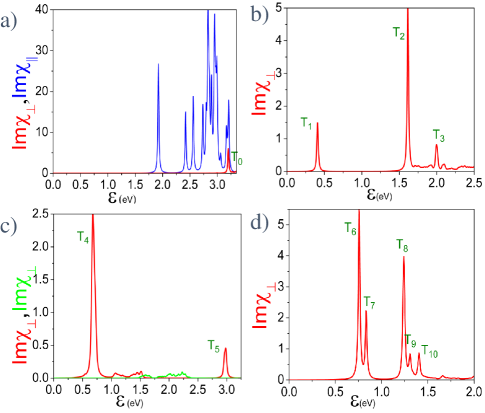
The qualitative picture based on the symmetry properties establishes the connection between the main features of spectrum of the bound states and the optical response. For example, for the Mo-vacancy the resonance in involves a bound state hidden in the valence band. In the case of S2-vacancy the symmetry analysis predicts that is featureless at low energies due to the smallness of , which is confirmed by the numerical calculations (see Fig. 4b). The Fermi level , however, can be shifted by means of a gate voltage to lie between equally degenerate states with different parities, which support transitions contributing to . Then should demonstrate a low-energy resonance. In the numerical simulations we modified the position of the Fermi level by adding charge to the whole layer by means of a charge concentration of cm-3, leading to a resonance in (see Fig. 4c). Fig. 4d shows the resonances due to transitions between states bound to MoS2.
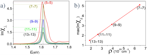
Considering the case when there is no overlap between bound states of neighboring VDs, we can use for the transition of a dilute gas of VDs Grynberg et al. (1970), where and are the concentration and number of VDs, respectively. denotes the dipole moment of the transition . This formula is in excellent agreement with the numerical calculations shown in Fig. 5 for supercell sizes from 7x7 up to 13x13. The peak for the 5x5 supercell does not follow this formula because the overlap between neighboring VDs is substantial, which leads to a peak shift and homogeneous peak broadening due to the formation of minibands. Additional inhomogeneous peak broadening is expected due to random distribution of VDs in the MoS2 SL.
Conclusion.
We show that in order to describe the electron states bound to VDs in MoS2 SLVD, it is necessary to consider odd states, which lead to the appearance of resonances in the out-of-plane optical response . Our results pave the way to the optical characterization of VDs in TMDC SLVD, which is of utmost importance for the future realization of high-performance electronic and optoelectronic devices based on TMDC SLs.
Acknowledgements.
Acknowledgments.
We acknowledge support provided by NSF grant ECCS-1128597. We thank Saiful Khondaker and Laurene Tetard for useful comments.
References
- Splendiani et al. (2010) A. Splendiani, L. Sun, Y. Zhang, T. Li, J. Kim, C.-Y. Chim, G. Galli, and F. Wang, Nano Lett. 10, 1271 (2010).
- Mak et al. (2010) K. F. Mak, C. Lee, J. Hone, J. Shan, and T. F. Heinz, Phys. Rev. Lett. 105, 136805 (2010).
- Zhu et al. (2011) Z. Y. Zhu, Y. C. Cheng, and U. Schwingenschlögl, Phys. Rev. B 84, 153402 (2011).
- Xiao et al. (2012) D. Xiao, G.-B. Liu, W. Feng, X. Xu, and W. Yao, Phys. Rev. Lett. 108, 196802 (2012).
- Lopez-Sanchez et al. (2013) O. Lopez-Sanchez, D. Lembke, M. Kayci, A. Radenovic, and A. Kis, Nat. Nanotechnol. 8, 497 (2013).
- Liu et al. (2013) G.-B. Liu, W.-Y. Shan, Y. Yao, W. Yao, and D. Xiao, Phys. Rev. B 88, 085433 (2013).
- Rostami et al. (2013) H. Rostami, A. G. Moghaddam, and R. Asgari, Phys. Rev. B 88, 085440 (2013).
- Pedersen et al. (2008) T. G. Pedersen, C. Flindt, J. Pedersen, N. A. Mortensen, A.-P. Jauho, and K. Pedersen, Phys. Rev. Lett. 100, 136804 (2008).
- Huang et al. (2013) Y. Huang, J. Wu, X. Xu, Y. Ho, G. Ni, Q. Zou, G. Koon, W. Zhao, A. Castro Neto, G. Eda, C. Shen, and B. Ozyilmaz, Nano Research 6, 200 (2013).
- Shao et al. (2014) L. Shao, G. Chen, H. Ye, Y. Wu, H. Niu, and Y. Zhu, J. Appl. Phys. 116, 113704 (2014).
- Islam et al. (2014) M. R. Islam, N. Kang, U. Bhanu, H. P. Paudel, M. Erementchouk, L. Tetard, M. N. Leuenberger, and S. I. Khondaker, Nanoscale 6, 10033 (2014).
- Kang et al. (2014) N. Kang, H. P. Paudel, M. N. Leuenberger, L. Tetard, and S. I. Khondaker, J. Phys. Chem. C 118, 21258 (2014).
- Zhou et al. (2013) Y. Zhou, P. Yang, H. Zu, F. Gao, and X. Zu, Phys. Chem. Chem. Phys. 15, 10385 (2013).
- Hong et al. (2015) J. Hong, Z. Hu, M. Probert, K. Li, D. Lv, X. Yang, L. Gu, N. Mao, Q. Feng, L. Xie, J. Zhang, D. Wu, Z. Zhang, C. Jin, W. Ji, X. Zhang, J. Yuan, and Z. Zhang, Nature Comm. 6, 6293 (2015).
- Le et al. (2014) D. Le, T. B. Rawal, and T. S. Rahman, J. Phys. Chem. C 118, 5346 (2014).
- Tao et al. (2003) J. Tao, J. P. Perdew, V. N. Staroverov, and G. E. Scuseria, Phys. Rev. Lett. 91, 146401 (2003).
- Faleev et al. (2004) S. V. Faleev, M. van Schilfgaarde, and T. Kotani, Phys. Rev. Lett. 93, 126406 (2004).
- Shishkin et al. (2007) M. Shishkin, M. Marsman, and G. Kresse, Phys. Rev. Lett. 99, 246403 (2007).
- (19) http://www.quantumwise.com/ .
- Cappelluti et al. (2013) E. Cappelluti, R. Roldán, J. A. Silva-Guillén, P. Ordejón, and F. Guinea, Phys. Rev. B 88, 075409 (2013).
- McCann and Fal’ko (2004) E. McCann and V. I. Fal’ko, J. Phys. Cond. Mat. 16, 2371 (2004).
- Akhmerov and Beenakker (2008) A. R. Akhmerov and C. W. J. Beenakker, Phys. Rev. B 77, 085423 (2008).
- Berry and Mondragon (1987) M. V. Berry and R. J. Mondragon, Proc. R. Soc. Lond. A 412, 53 (1987).
- Rose et al. (2013) F. Rose, M. O. Goerbig, and F. Piéchon, Phys. Rev. B 88, 125438 (2013).
- Harrison (1970) W. A. Harrison, Solid state theory (McGraw-Hill, New York, 1970).
- Grynberg et al. (1970) G. Grynberg, A. Aspect, and C. Fabre, An Introduction to Quantum Optics (Cambridge University Press, Cambridge, 1970).