Ag and Au Atoms Intercalated in Bilayer Heterostructures of Transition Metal Dichalcogenides and Graphene
Abstract
The diffusive motion of metal nanoparticles Au and Ag on monolayer and between bilayer heterostructures of transition metal dichalcogenides and graphene are investigated in the framework of density functional theory. We found that the minimum energy barriers for diffusion and the possibility of cluster formation depend strongly on both the type of nanoparticle and the type of monolayers and bilayers. Moreover, the tendency to form clusters of Ag and Au can be tuned by creating various bilayers. Tunability of the diffusion characteristics of adatoms in van der Waals heterostructures holds promise for controllable growth of nanostructures.
pacs:
73.20.Hb, 82.45.Mp, 73.61.-r, 73.90.+f, 74.78.FkI Introduction
In recent years graphenenovoselov2004electric has become one of the most attractive materials due to its unique properties such as high-mobility electron transport novoselov2005two ; bolotin2008temperature , the presence of room-temperature quantum Hall effectnovoselov2007room , the strong lattice structurelee2008measurement and the extremely high in-plane thermal conductivity.seol2010two However, its highly active surface and the lack of a band gap in the electronic structure are emerging drawbacks for graphene. Recently, interests have now also focused on other two-dimensional systems having honeycomb structures, such as graphanesofo2007graphane ; flores2009graphene , halogenated graphenesnair2010fluorographene ; hasan-cf ; ortwin-cf ; hasan-ccl , silicenekara2012review , III-V binary compoundsPhysRevB.52.8881 , and transition metal dichalcogenides (TMDs)PhysRevB.8.3719 ; chhowalla2013chemistry ; yandong1 ; hasan-nature . Recent studies have revealed that among various monolayer structures especially TMDs are quite promising materials for electronics and optoelectronics applications.
Bulk TMDs have a number of exceptional properties such as superconductivity of TaS2 and NbSe2, Mott transition in 1T-TaS2 and the presence of charge density wave in TiSe2. sipos2008mott ; jishi2008electronic It was also reported that the electrical and optical properties of TMDs are dramatically altered with the number of layerssplendiani2010emerging ; PhysRevB.88.075409 ; hasan-wse2 . Although bulk hexagonal TMDs possess an indirect band gap, mono-layer TMDs exhibit a direct band gap which is crucial for optoelectronic devices, sensors and catalysts. In addition, n-type and p-type field-effect-transistors (FETs) based on monolayer and multilayer TMDs have been investigated.das2012high ; radisavljevic2011single ; fang2012high It was also reported that many monolayer 2D crystals are reactive and segregation may occur easily.geim2011random Therefore, the investigation of bilayer structures which are chemically more stable than monolayer structures is of vital significance. Recent studies have shown that synthesis of heterostructures made of combinations of different TMD single layers, graphene, fluorographene and hexagonal-BN (hBN) is experimentally achievable.geim2013van ; terrones2013novel ; haigh2012cross ; britnell2012field ; dean2012graphene ; georgiou2012vertical Since TMDs and other two-dimensional structures have a lot of diverse monolayer structures, when they are combined together they are expected to exhibit very different properties. yandong ; xinru
Since the intercalation and migration of foreign atoms is inevitable during the formation of such lamellar materials and heterostructures, the investigation of the diffusion characteristics of various impurities is essential. Early studies revealed that alkali-metal doping of bulk TiSe2 and MoS2 can be utilized as an efficient way to tune the Fermi level.joensen1986single ; jaegermann1994photoelectron The electrical conductivity of MoS2 can be altered by substitutional doping.tiong2001electrical ; PhysRevB.78.134104 Furthermore, decoration of the surfaces of few layer TMDs by metal nanoparticles like Au, Ag and Pt may provide p- and n-type doping.rao2012recent ; shi2013selective ; kim2013enhanced ; duygu The metal-atom adsorbed TMDs find their application in various areas including energy storagematte2012synthesis , photonicshuang2010actively ; qian2012atomically , biosensinghe2012graphene , and catalysis.lu2010platinum In a recent study, it has been demonstrated that, the presence of various impurities at the interface between MoS2/graphene/hBN and WS2/graphene/hBN heterostructures may modify the mobility of charge carriers.Kretinin It was also reported that contamination and migration of various molecules are inevitable during the formation of graphene based heterostructures and trapped hydrocarbons segregate into isolated pockets, leaving the rest of the interface atomically clean. Haigh In addition, it was found that, attached metal nanoparticles on TMDs/Graphene stacks can be suitable for enhanced optoelectronic properties.britnell2013strong ; Sachs
Despite some recent studies on adatom adsorption on various TMDs, intercalation and migration of foreign atoms in heterostructures have not been investigated. In this study, using density functional theory based electronic structure method, we investigate the diffusion characteristics of heavy metal atoms (Au and Ag) on monolayers and intercalated in such bilayer heterostructures. The paper is organized as follows: In Sec. II we give details of our computational methodology. In Sec. III the energetics of the metal atoms Ag and Au on monolayers of graphene and TMDs are presented. In Sec. IV diffusion characteristics of those metal atoms inside bilayer heterostructures are shown and in Sec. V we summarize and conclude our results.
II Computational Methodology
To determine ground state atomic structures and migration characteristics of monolayers and their bilayer heterostructures, first-principles calculations were performed using density functional theory (DFT) with a plane-wave basis set as implemented in the Vienna ab initio simulation package (VASP).PhysRevB.54.11169 For the exchange correlation function generalized gradient approximation (GGA) of Perdew, Burke and ErnzerhofPhysRevLett.77.3865 was used together with the van der Waals correction.grimme2006semiempirical Spin-unpolarized calculations were carried out using projector-augmented-wave potentials (PAW). The plane-wave basis set with kinetic energy cutoff of 500 eV was used.
A 44 and 33 hexagonal supercells of single layer and bilayer structures are employed to model diffusion paths of metal atoms, respectively. The k-point samples were 331 for these supercells. It is calculated that a 12 Å of vacuum space is enough to hinder long-range dispersion forces between two adjacent images in the supercell. Lattice constants and total energies were computed with the conjugate gradient method, where atomic forces and total energies were minimized. The convergence criterion of our calculations for ionic relaxations is eV between two consecutive steps. The maximum Hellmann-Feynman forces acting on each atom were reduced to a value of less than eV/Å. All components of the external pressure in the unit cell was held below 1 kbar. For the electronic density of states Gaussian smearing was used with a broadening of 0.1 eV. The non-local correlation energies were determined by employing density functional theory plus the long-range dispersion correction (DFT+D2) method.grimme2006semiempirical The values of 24.670, 5.570, 12.640, 1.750, 24.670, 40.620, and 40.620 are used as the C6 coefficient of Mo, S, Se, C, Ag, Au, and W atoms, respectively. On the other hand, values of 1.639, 1.683, 1.771, 1.452, 1.639, 1.772, and 1.772 are used for the vdW radius of Mo, S, Se, C, Ag, Au, and W atoms, respectively. These C6 coefficients and vdW radii were determined from previous studies. grimme2006semiempirical ; amft It is essential that long-range dispersion correction to the interlayer force is taken into account in order to obtain reliable layer-layer distances and electronic properties of the heterobilayers.
To study the adsorption and diffusion of metal atoms in these systems, total energies of monolayer TMDs (graphene) with adatom were calculated for 19 (12) different points which include the high symmetry points (H, M, B, and T). Total energies of bilayers with adatom were calculated for only 4 high symmetry points. In these different points, the adatom-surface distance was fully relaxed while the position of the adatoms parallel to the surface was kept fixed. To obtain accurate diffusion characteristics of heavy atoms on monolayer TMDs and graphene, calculations were performed using 4x4 supercells. In these calculations, first and second nearest neighbors of the adatom were fully relaxed while all the rest was kept fixed. On the other hand, in the bilayer calculations, all atoms of bilayers were free to move in all directions. Binding energies were calculated for the most favorable adsorption sites. These binding energies were calculated from the expression , where EB is the binding energy of the metal atoms on the TMDs or graphene, EMonolayer is the energy of monolayer TMDs or graphene, EA is the energy of metal atoms, EMonolayer+A is the total energy of the metal atom-monolayer system.
We have chosen the following convention to define the diffusion energy barrier. The binding energy of an adatom was calculated at all high-symmetry points of the TMDs and the graphene surface. Since adatoms follow the lowest energy path, the difference of the energies between the most favorable site and the second most favorable site was considered as the diffusion energy barrier.
In order to obtain the correct value of the charge transferred between the metal atoms, the TMDs and the graphene, Bader charge analysis was performed. Rather than electronic orbitals in Bader methodology, charge partitioning is based on electronic charge density and therefore it is highly efficient, it scales linearly with the number of grid points, and is more robust than other partitioning schemes.henkelman2006fast ; tang2009grid ; sanville2007improved
III Diffusion of Heavy Atoms on Monolayers of TMDs and graphene
So far, experiments have revealed that similar to graphene many of the TMDs (MoS2, MoSe2, WS2, WSe2, ReS2) have a lamellar crystal structure where the layers are held together by weak van der Waals forces, while intra-layer metal-chalcogen bonds have strong covalent character. Due to the weakly (vdW) bonded layered structure of graphene and TMDs either diffusion of foreign atoms on their surface or easy intercalation into the layers may take place. Moreover, these foreign atoms may provide new functionalities to the TMDs and to the heterostructures made of various layered materials. Therefore, understanding how foreign atoms adsorb, migrate and intercalate are of highly importance.
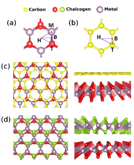
First we calculate the binding and migration of Ag and Au atoms on the surface of monolayer TMDs and graphene. For a hexagonal primitive unitcell of MoS2, MoSe2, WS2 and graphene the lattice parameters are calculated to be 3.190, 3.316, 3.179 and 2.468 Å, respectively. For calculations of adsorption and migration of metal atoms 44 supercells were used in order to limit Au-Au (and Ag-Ag) interaction between adjacent cells. As shown in Fig. 1 for a metal atom adsorbed on TMDs and graphene, there are four possible adsorption sites: top of carbon or chalcogen atom (T), bridge site on C-C or M-X bond (B), on top of the center of hollow site (H) and on top of metal atom Mo or W (M).
Diffusion and mobility of impurities on a two-dimensional crystal surface can be described by quantities such as activation energy () and jump probability () from the binding site over the lowest-barrier path at room temperature. The value is a measure of the possibility of propagation by overcoming the energy barrier among the possible adsorption sites. Jump probability from one lattice site to another one can be calculated by using the formula where is the Boltzmann constant and it increases exponentially with increasing temperature. Here is the activation energy which is equal to the difference of the energy of the two lowest energy states.
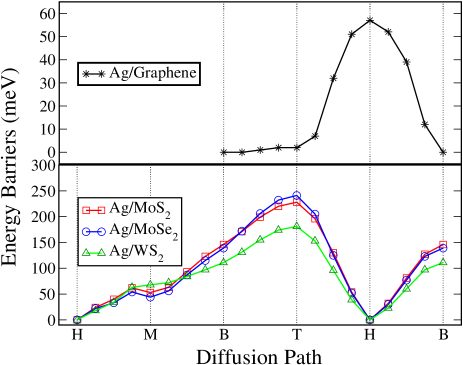
Our calculated adsorption sites, binding energies, vertical adsorption position, charge transfer, energy barrier and jump probability () values are listed in Table 1. We see that the bonding of an Ag atom to graphene occurs at the B site and the H site is the least favorable adsorption site. In accordance with the previous DFT study, we found that the binding energy of Au on graphene is almost twice the binding energy of Ag on graphene. The Ag atoms lose (while the Au atoms gain) a small amount of charge when they bind to the graphene surface.Nakada On the surface of TMDs, the most favorable bonding site for Ag atoms is the H site and the next largest adsorption energy is found for the M site. It is reasonable to assume that metal atoms diffuse through these two favorable adsorption sites. Therefore the energy difference between these two lowest-energy sites can be regarded as the diffusion barrier. Since the energy barrier for Ag between H and M sites is high (50 meV) diffusion through these symmetry points may not occur at low temperatures. It appears from Fig. 2 that Ag atoms on graphene migrate through the B and T sites with almost zero (2 meV) energy barrier, while migration on TMDs (MoS2, MoSe2 and WS2) occurs through H and M sites. As shown in Table 1, room temperature values of Ag atoms are 0.129, 0.182, 0.072 and 0.926 for MoS2, MoSe2, WS2 and graphene, respectively. Thus diffusion of the Ag atoms on graphene occurs much more easily than on TMDs.
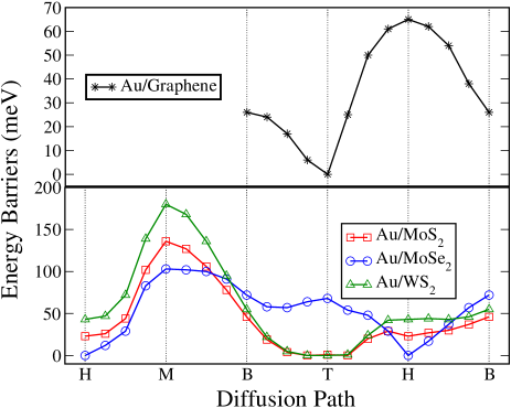
Binding energy of a single Au atom on graphene and TMDs is found to be 300 meV larger than that of Ag. Interestingly, on MoSe2, Au atoms prefer bonding on the H site like Ag atoms, while the top of a sulfur atom (T site) is the most preferable site on MoS2 and WS2 layers. The distinctive behavior of the Au atoms can be explained by the distinctive characteristic of the S-Au bond. Although the chemical properties of chalcogen atoms S and Se are quite similar, as shown by Yee et al.Yee , the strength of the S-Au bond is slightly weaker than the Se-Au bond. Our calculations reveal that the binding energy of an Au atom on MoSe2 surface is higher than the binding energy of an Au atom on MoS2 and WS2 surfaces. Interestingly, strong Au-S bonds require bonding on T site while the Au-Se bond results in H-site adsorption. As shown in Fig.3, as in the Ag adsorption case, MoS2 and WS2 surfaces have almost identical characteristics for Au adsorption at all high symmetry points. In addition, the migration barrier seen by Au atoms is 30 meV larger than the energy barrier of Ag atoms on graphene. Therefore, compared to Ag on graphene, the smaller jump probability of Au atoms on graphene implies relatively slow and smaller nucleation of Au clusters on graphene which agrees with experimental results.Subrahmanyam
| Ag/MoS2 | Ag/MoSe2 | Ag/WS2 | Ag/Graphene | |
|---|---|---|---|---|
| Binding Site | H | H | H | B |
| Binding energy (eV) | 0.943 | 0.928 | 0.845 | 0.360 |
| Height (Å) | 1.97 | 2.07 | 2.04 | 2.57 |
| (e) | -0.30 | -0.18 | -0.23 | -0.16 |
| Energy Barrier (meV) | 53(M), 146(B), 228(T) | 44(M), 139(B), 241(T) | 68(M), 111(B), 181(T) | 2(T), 57(H) |
| Jump probability () | 0.129 | 0.182 | 0.072 | 0.926 |
| Au/MoS2 | Au/MoSe2 | Au/WS2 | Au/Graphene | |
| Binding Site | T | H | T | T |
| Binding energy (eV) | 1.161 | 1.232 | 1.146 | 0.633 |
| Height (Å) | 2.26 | 2.03 | 2.27 | 2.56 |
| (e) | 0.01 | 0.08 | 0.06 | 0.22 |
| Energy Barrier (meV) | 136(M), 23(H), 46(B) | 103(M), 72(B), 68(T) | 180(M), 43(H), 55(B) | 65(H), 26(B) |
| Jump probability () | 0.411 | 0.072 | 0.189 | 0.366 |
Calculated room temperature values of an Au atom on MoS2, MoSe2, WS2 and graphene surfaces are 0.411, 0.072, 0.189 and 0.366, respectively. Au atom has the maximum value on a MoS2 surface, whereas it has the minimum value on a MoSe2 surface. values of Au atoms on a MoS2 surface is higher than that of Ag atoms. This result is consistent with the previous experimental study where they found that the cluster diameter of Au and Ag atoms on MoS2 were found to be 14 and 6 nm, respectively. Bolla Other experimental work showed that cluster diameters of Au and Ag atoms on WS2 are 19-20 and 5 nm, respectively.matte2012synthesis In agreement with this experimental study, our calculations show that the value of the Au atoms on a WS2 surface is higher than that of Ag atoms.
IV Diffusion of Heavy Atoms Intercalated Between Van der Waals Bilayers
The vertical stacking of graphene and other two-dimensional atomic crystals allows for the combination of different electronic properties. Recent studies have shown that, electronic and optical properties of TMDs can be altered dramatically by forming such heterostructures.geim2013van ; komsa2013electronic It appears that the intercalation and contamination of foreign atoms and functional groups at the interface of these heterostructures are unavoidable. As shown by recent experimental study, heavy atoms such as Au and Ag are quite mobile on TMD surfaces and they form clusters. Gong Therefore, understanding the diffusion characteristics of heavy atoms at the interface of these heterostructures is of importance for the ongoing research on heterostructure devices.
In this section, we investigate the diffusion characteristics of Au and Ag atoms intercalated in MoS2/Graphene, MoS2/MoS2, MoS2/MoSe2 and MoS2/WS2 heterostructures.
IV.1 Diffusion through MoS2/Graphene Bilayer Heterostructure
First, we start with the heterostructure MoS2/Graphene. However, the determination of the most favorable atomic structure of MoS2/Graphene heterostructure is more complicated due to the lattice mismatch. Our calculations showed that bare DFT calculations are not capable of finding the ground state ordering of graphene placed on MoS2 due to the presence of many local minima corresponding to metastable states. It was seen that low-temperature (100 K) molecular dynamic calculations are able to avoid local minima allowing to obtain the relaxed geometric structure of MoS2/Graphene as shown in Fig. 1(c). Due to the lack of symmetry in the MoS2/Graphene structure, twenty-seven inequivalent adsorption sites are considered for each Ag (and Au) atom adsorption. Table 2 lists the intercalation energies obtained by using a 33 unit cell of the most favorable site for each configuration. Here the intercalation energy is defined by the expression
| (1) |
where is the intercalation energy of Ag(Au) atom, is the energy of the metal-atom heterobilayer system, is the energy of heterobilayers and is the energy of the adatom. Due to the large binding energies of adatoms on MoS2, all the equilibrium geometries are ruled by MoS2 except for the MoS2/Au/MoSe2 structure where Au’s binding is larger with the MoSe2 layer.
Our calculations revealed that binding energies of Ag and Au atoms on TMD substrates are larger than that on graphene and Au atoms are more stable than Ag atoms on these monolayers. For the simulation of the MoS2/Graphene heterostructure we considered 44 and 33 unit cells for graphene and MoS2 layers, respectively. After full optimization, the lattice parameter of the heterostructure is calculated to be 9.791 Å. For this supercell the maximum lattice mismatch is 3.
The adsorption energies and the equilibrium geometries were calculated by considering 27 different adsorption sites for each Ag and Au atoms at the MoS2/Graphene interface. It is seen that the most favorable site of Ag atoms on MoS2 is changed from H to M site upon the addition of the graphene layer. Energy barrier of Ag atoms is enhanced from 2 to 43 meV with graphene layer. Although the energy barriers seen by Au atom on MoS2 are significantly enhanced by the presence of the graphene layer, the T site of MoS2 remains as the most favorable adsorption site of Au.
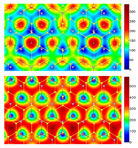
Furthermore, we show 2D plots of the energy barriers seen by Ag and Au atoms at the MoS2/Graphene interface in Fig. 4. It is clear that Ag and Au atoms have entirely different diffusion characteristics at the MoS2/Graphene interface: (i) diffusion of Ag atoms are much easier while Au atoms may diffuse at high temperatures, (ii) diffusion of an Ag atom occurs through the bridge sites of the top-lying graphene layer, (iii) diffusion of Au atom may occur from one top-sulfur site to another one through the top site of Mo atoms. Here, similar characteristic diffusion behavior of heavy atoms can be expected for bilayer heterostructures of WS2/Graphene as well.
| MoS2/Ag/MoS2 | MoS2/Ag/MoSe2 | MoS2/Ag/WS2 | MoS2/Ag/Graphene | |
|---|---|---|---|---|
| Binding Site | H | H | H | M |
| Intercalation Energy (eV) | -1.461 | -1.395 | -1.319 | -1.344 |
| Height above MoS2 (Å) | 1.85 | 1.71 | 1.85 | 1.61 |
| (e) | -0.42 | -0.41 | -0.41 | -0.47 |
| LL Distance (pristine, with Ag) | 3.08, 3.70 | 3.10, 3.60 | 3.09, 3.71 | 3.32, 3.86 |
| Energy Barrier (meV) | 222(M), 282(B) | 206(M), 308(B) | 243(M), 295(B) | 43(H), 196(T) |
| 222(T) | 274(T) | 340(T) | ||
| Jump probability () | 210-4 | 3.510-4 | 810-5 | 0.189 |
| MoS2/Au/MoS2 | MoS2/Au/MoSe2 | MoS2/Au/WS2 | MoS2/Au/Graphene | |
| Binding Site | B | H | H | T |
| Intercalation Energy (eV) | -1.645 | -1.562 | -1.504 | -1.541 |
| Height above MoS2 (Å) | 2.07 | 1.79 | 1.85 | 2.07 |
| (e) | -0.15 | -0.13 | -0.18 | -0.21 |
| LL Distance (pristine, with Au) | 3.08, 4.12 | 3.10, 3.72 | 3.09, 3.74 | 3.32, 4.35 |
| Energy Barrier (meV) | 12(H), 96(M), 95(T) | 118(M), 75(B), 103(T) | 78(M), 24(B), 164(T) | 468(H) 326(M) |
| Jump probability () | 0.628 | 0.055 | 0.395 | 310-6 |
IV.2 Diffusion through MX2/MX2 Bilayer Heterostructures
Next we investigate the diffusion and energy barriers which are seen by Ag and Au atoms sandwiched in between single layers of TMDs. There are two possible stacking types for bilayer TMDs; AA and AB stacking. In the AA stacking, the chalcogen atom (S or Se) in one layer is on top of the chalcogen atom (S or Se) of the other layer. On the other hand, in AB stacking, chalcogen atom (S or Se) in one layer is on top of the metal atoms (Mo or W) of the other layer. Our calculations show that for the considered bilayer heterostructures of TMDs, the AB stacking is the ground state geometry.
MoS2/MoS2 Bilayers: The lattice parameter of AB-stacked bilayer MoS2/MoS2 structure was found to be almost the same as of monolayer MoS2. It is seen that the Ag-MoS2 distance decreases due to the presence of the upper MoS2 layer. The layer-layer distance of bilayer MoS2 increases from 3.08 to 3.70 Å upon single Ag intercalation. On the other hand, single Au atom causes a larger layer separation (from 3.08 to 4.12 Å) than Ag atoms. Our calculations revealed that the most preferable site of the Ag atom remains the H-site, even after the addition of the second layer. Our charge analysis showed that metal atoms tend to donate a larger amount of charge when they are intercalated in bilayers. The amount of charge transfer becomes 0.42 and 0.15 for Ag and Au atoms, respectively. However, it is worthwhile to note that the preferable adsorption site for Au atoms changes from T to B site. Au atoms tend to bind with two S atoms that are in two different layers. For this reason, the B-site is the most favorable site.
The minimum diffusion barrier of Ag atom is increased by 170 meV after the addition of the second layer. Interestingly diffusion barriers of the Ag atom between bilayer MoS2 from H to M and H to T sites are the same. The minimum diffusion barrier of Au atom is reduced by half when a second layer is added. These results show that the diffusion behavior of Ag and Au atoms between bilayer MoS2 are completely different. Ag atoms are not likely to form clusters inside the bilayer MoS2. On the other hand, Au atoms may form clusters between two MoS2 layers and the clusterization weight of them is larger than that on single layer of MoS2.
MoS2/MoSe2 Bilayers: For the geometry optimization of the MoS2/MoSe2 bilayer structure we performed full atomic and lattice parameter relaxation and therefore internal strain due to lattice mismatch is lowered to less than 1 kB. The lattice parameter of MoS2/MoSe2 is calculated to be 3.252 Å. For this lattice parameter, the maximum lattice mismatch is 2 which is in the range of experimentally available strain values. When Au and Ag atoms are intercalated between MoS2/MoSe2, they show the same trend; their height above the MoS2 surface are fairly close (1.7 Å for Ag and 1.8 Å for Au) and the layer-layer distance increases from 3.1 to 3.6 and 3.7 Å for Ag and Au, respectively. H-site is the most favorable site for Ag and Au atoms when they are located between MoS2/MoSe2 bilayer. When Ag atom is inserted in MoS2/MoSe2, it donates 0.41 to neighboring TMD layers. It appears that the majority of the charges are transfered to the MoS2 layer. Similarly the Au atom loses 0.13 charge when inserted between MoS2/MoSe2. The minimum diffusion barrier of Ag atom is increased by 150 meV when the second layer is present. But the second favorable site does not change with the addition of the MoSe2 layer (M). The minimum diffusion barrier of Au atom increases from 23 to 75 meV with MoSe2 addition. Second favorable site of Au atom changes from H to B site when MoSe2 layer is added. Similar to MoS2/MoS2, the jump probability of Ag atom becomes zero with the addition of MoSe2 as a second layer. The value of Au atom decreases from 0.411 to 0.055 with the addition of MoSe2 layer. Therefore, the formation of Ag cluster between MoS2/MoSe2 bilayer heterostructure is hindered by the presence of the second layer. The nucleation of Au clusters may happen with a slower nucleation rate in MoS2/MoSe2 as compared to monolayer MoS2.
MoS2/WS2 Bilayers: The lattice mismatch between MoS2 and WS2 is negligible and the lattice parameter of the bilayer structure was calculated to be 3.182 Å. Both Au and Ag atoms prefer to be bonded on the H site 1.85 Å away from the surface of MoS2. When Ag and Au atoms are inserted between MoS2/WS2, the interlayer distances increase from 3.09 to 3.71 and 3.74 Å, respectively. We found that the Ag atom donates 0.41 to the surrounding MoS2/WS2 bilayer structure whereas the amount of charge transfer is 0.18 for Au. The minimum diffusion barrier of the Ag atom increases 190 meV with the addition of WS2 layer, but it does not change the second favorable site of Ag atom (M). It is seen that the addition of the WS2 layer does not have any significant effect on the minimum diffusion barrier of the Au atom.
In this case, the change of the value of the Ag atom shows the same trend with bilayer MoS2 and MoS2/MoSe2. In these cases, the value of Ag atom becomes zero with the addition of the second layer (WS2 in this case). On the other hand, addition of a WS2 layer does not change the value of the Au atom between MoS2/WS2, significantly. As a result, Ag atoms are not likely to form clusters when intercalated in MoS2/WS2, while the clusterization probability of Au atoms does almost not change with WS2 layer addition.
V Conclusion
We found that the binding energy of Ag and Au atoms is maximum when they are placed on MoS2 and MoSe2, respectively and the binding energy of these atoms on graphene is lower than that on TMDs. Ag atoms prefer to bind at the H site on TMDs, while the H and the T sites are most favorable adsorption sites for Au atoms. Just as for the Ag atom, Au atom binds to H site on MoSe2. However, Au atom binds to T site on MoS2 and WS2. When Ag atom adsorbs on these monolayers, it tends to donate charge, whereas Au atom tends to receive charge from these monolayers. Calculated values revealed that, clusterization tendency of Ag and Au are the largest on graphene and MoS2 layers, respectively.
Addition of a second layer has a considerable effect on the diffusion phenomena of Ag and Au atoms. Ag atom binds to H site of all TMDs heterostructures, whereas it binds to M site of the MoS2/Graphene heterostructure. When an Au atom is inserted between MoS2/MoSe2 and MoS2/WS2 heterostructures, H site is the energetically most favorable site. B and T sites are the most favorable sites for the Au atom when it is placed between MoS2/MoS2 and MoS2/Graphene heterostructures. The clusterization probability of Ag atom becomes zero when TMDs are added as a second layer. On the other hand, the value of Ag atom increases with the addition of a graphene layer. Addition of a graphene layer hinders diffusion of Au atom. WS2 addition as a second layer, does not make a significant effect on the cluster formation probability of Au atom. Addition of MoSe2 as a second layer reduces the clusterization of Au, whereas the addition of a second MoS2 layer increases it. Our calculated intercalation energies showed that, when Au and Ag atoms are inserted between MoS2/Graphene, MoS2/MoS2, MoS2/MoSe2 or MoS2/WS2, they are energetically more stable as compared to the case where Ag and Au atoms are adsorbed on the monolayer substrates. The energy barrier for Au atoms is lower than the one for Ag atoms, when they are inserted between TMD heterostructures. On the other hand, the energy barrier of Ag atoms is lower than the energy barrier of Au atoms when they are inserted between MoS2/Graphene. Tunability of diffusion barriers seen by adatoms in van der Waals heterostructures makes these materials potential hosts for controlled growth of nanoclusters.
Acknowledgements.
This work was supported by the Flemish Science Foundation (FWO-Vl) and the Methusalem foundation of the Flemish government. Computational resources were provided by TUBITAK ULAKBIM, High Performance and Grid Computing Center (TR-Grid e-Infrastructure), and HPC infrastructure of the University of Antwerp (CalcUA) a division of the Flemish Supercomputer Center (VSC), which is funded by the Hercules foundation. H.S. is supported by a FWO Pegasus Marie Curie Fellowship. F.I. and R.T.S. acknowledge the support from TUBITAK project 111T318.References
- (1) K. S. Novoselov, A. K. Geim, S. V. Morozov, D. Jiang, Y. Zhang, S. V. Dubonos, I. V. Grigorieva, and A. A. Firsov, Science 306, 666 (2004).
- (2) K. S. Novoselov, A. K. Geim, S. V. Morozov, D. Jiang, M. I. Katsnelson, I. V. Grigorieva, S. V. Dubonos, and A. A. Firsov, Nature 438, 197 (2005).
- (3) K. I. Bolotin, K. J. Sikes, J. Hone, H. L. Stormer, and P. Kim, Phys. Rev. Lett. 101, 096802 (2008).
- (4) K. S. Novoselov, Z. Jiang, Y. Zhang, S. V. Morozov, H. L. Stormer, U. Zeitler, J. C. Maan, G. S. Boebinger, P. Kim, and A. K. Geim, Science 315, 1379 (2007).
- (5) C. Lee, X. Wei, J. W. Kysar, and J. Hone, Science 321, 385 (2008).
- (6) J. H. Seol, I. Jo, A. L. Moore, L. Lindsay, Z. H. Aitken, M. T. Pettes, X. Li, Z. Yao, R. Huang, D. Broido, N. Mingo, R. S. Ruoff, and L. Shi, Science 328, 213 (2010).
- (7) J. O. Sofo, A. S. Chaudhari, and G. D. Barber, Phys. Rev. B 75, 153401 (2007).
- (8) M. Z. S. Flores, P. A. S. Autreto, S. B. Legoas, and D. S. Galvao, Nanotechnol. 20, 465704 (2009).
- (9) R. R. Nair, W. Ren, R. Jalil, I. Riaz, V. G. Kravets, L. Britnell, P. Blake, F. Schedin, A. S. Mayorov, S. Yuan, M. I. Katsnelson, H. M. Cheng, W. Strupinski, L. G. Bulusheva, A. V. Okotrub, I. V. Grigorieva, A. N. Grigorenko, K. S. Novoselov, and A. K. Geim, Small 6, 2877 (2010).
- (10) H. Sahin, M. Topsakal, and S. Ciraci, Phys. Rev. B 83, 115432 (2011).
- (11) H. Peelaers, A. D. Hernandez-Nieves, O. Leenaerts, B. Partoens, and F. M. Peeters, Appl. Phys. Lett. 98, 051914 (2011).
- (12) H. Sahin, and S. Ciraci, J. Phys. Chem. C 116, 24075 (2012).
- (13) A. Kara, H. Enriquez, A. P. Seitsonen, L. C. L. Y. Voon, S. Vizzini, B. Aufray, and H. Oughaddou, Surf. Sci. Rep. 67, 1 (2012).
- (14) H. Sahin, S. Cahangirov, M. Topsakal, E. Bekaroglu, E. Akturk, R. T. Senger, and S. Ciraci Phys. Rev. B 80, 155453 (2009).
- (15) L. F. Mattheiss, Phys. Rev. B 8, 3719 (1973).
- (16) M. Chhowalla, H. S. Shin, G. Eda, L. J. Li, K. P. Loh, and H. Zhang, Nat. Chem. 5, 263 (2013).
- (17) Y. Ma, Y. Dai, M. Guo, C. Niu, Y. Zhu, and B. Huang, ACS Nano 6 (2), 1695 (2012).
- (18) S. Tongay, H. Sahin, C. Ko, A. Luce, W. Fan, K. Liu, J. Zhou, Y. S. Huang, C. H. Ho, J. Yan, D. F. Ogletree, S. Aloni, J. Ji, S. Li, J. Li, F. M. Peeters, and J. Wu, Nat. Commun. 5, 3252 (2014).
- (19) B. Sipos, A. F. Kusmartseva, A. Akrap, H. Berger, L. Forro, and E. Tutis, Nat. Mater. 7, 960 (2008).
- (20) R. A. Jishi, and H. M. Alyahyaei, Phys. Rev. B 78, 144516 (2008).
- (21) A. Splendiani, L. Sun, Y. Zhang, T. Li, J. Kim, C. Y. Chim, G. Galli, and F. Wang, Nano Lett. 10, 1271 (2010).
- (22) E. Cappelluti, R. Roldan, J. A. Silva-Guillen, P. Ordejon, and F. Guinea, Phys. Rev. B 88, 075409 (2013).
- (23) H. Sahin, S. Tongay, S. Horzum, W. Fan, J. Zhou, J. Li, J. Wu, and F. M. Peeters, Phys. Rev. B 87, 165409 (2013).
- (24) S. Das, H. Y. Chen, A. V. Penumatcha, and J. Appenzeller, Nano Lett. 13, 100 (2013).
- (25) B. Radisavljevic, A. Radenovic, J. Brivio, V. Giacometti, and A. Kis, Nat. Nanotechnol. 6, 147 (2011).
- (26) H. Fang, S. Chuang, T. C. Chang, K. Takei, T. Takahashi, and A. Javey, Nano Lett. 12, 3788 (2012).
- (27) A. K. Geim, Intern. J. Mod. Phys. B 25, 4055 (2011).
- (28) A. K. Geim, and I. V. Grigorieva, Nature 499, 419 (2013).
- (29) H. Terrones, F. López-Urías, and M. Terrones, Sci. Rep. 3, 1549 (2013).
- (30) S. J. Haigh, A. Gholinia, R. Jalil, S. Romani, L. Britnell, D. C. Elias, K. S. Novoselov, L. A. Ponomarenko, A. K. Geim, and R. Gorbachev, Nat. Mat. 11, 764 (2012).
- (31) L. Britnell, R. V. Gorbachev, R. Jalil, B. D. Belle, F. Schedin, A. Mishchenko, T. Georgiou, M. I. Katsnelson, L. Eaves, S. V. Morozov, N. M. R. Peres, J. Leist, A. K. Geim, K. S. Novoselov and L. A. Ponomarenko Science 335, 947 (2012).
- (32) C. Dean, A. F. Young, L. Wang, I. Meric, G. H. Lee, K. Watanabe, T. Taniguchi, K. Shepard, P. Kim, and J. Hone, Solid State Commun. 152, 1275 (2012).
- (33) T. Georgiou, R. Jalil, B. D. Belle, L. Britnell, R. V. Gorbachev, S. V. Morozov, Y. J. Kim, A. Gholinia, S. J. Haigh, O. Makarovsky, L. Eaves, L. A. Ponomarenko, A. K. Geim, K. S. Novoselov and A. Mishchenko, Nat. Nanotechnol. 8, 100 (2012).
- (34) Y. Ma, Y. Dai, W. Wei, C. Niu, L. Yu, and B. Huang, J. Phys. Chem. C 115 (41), 20237 (2011).
- (35) X. Li, Y. Dai, Y. Ma, S. Han, and B. Huang, Phys. Chem. Chem. Phys. 16, 4230 (2014).
- (36) P. Joensen, R. F. Frindt, and S. R. Morrison, Mat. Res. Bullet. 21, 457 (1986).
- (37) W. Jaegermann, C. H. Pettenkofer, A. Schellenberger, C. A. Papageorgopoulos, M. Kamaratos, D. Vlachos, and Y. Tomm, Chem. Phys. Lett. 221, 441 (1994).
- (38) K. K. Tiong, Y. S. Huang, and C. H. Ho, Journal of Alloys and Compounds 317, 208 (2001).
- (39) V. V. Ivanovskaya, A. Zobelli, A. Gloter, N. Brun, V. Serin, and C. Colliex, Phys. Rev. B 78, 134104 (2008).
- (40) C. N. R. Rao, H. S. S. R. Matte, R. Voggu, and A. Govindaraj, Dalton Transactions 41, 5089 (2012).
- (41) Y. Shi, J. K. Huang, L. Jin, Y. T. Hsu, S. F. Yu, L. J. Li, and H. Y. Yang, Sci. Rep. 3, 1839 (2013).
- (42) J. Kim, S. Byun, A. J. Smith, J. Yu, and J. Huang, J. Phys. Chem. Lett. 4, 1227 (2013).
- (43) H. D. Ozaydin, H. Sahin, R. T. Senger, and F. M. Peeters, Article first published online: 16 JUN 2014, DOI: 10.1002/andp.201400079
- (44) H. S. S. Matte, U. Maitra, P. Kumar, B. G. Rao, K. Pramoda, and C.N.R. Rao, Zeitschrift für Anorganische und Allgemeine Chemie 638, 2617 (2012).
- (45) F. Huang, and J. J. Baumberg, Nano Lett. 10, 1787 (2010).
- (46) H. Qian, Y. Zhu, and R. Jin, Proceedings of the National Academy of Sciences 109, 696 (2012).
- (47) S. He, K. K. Liu, S. Su, J. Yan, X. Mao, D. Wang, Y. He, L. J. Li, S. Song, and C. Fan, Analytical Chem. 84, 4622 (2012).
- (48) Y. C. Lu, Z. Xu, H. A. Gasteiger, S. Chen, K. Hamad-Schifferli, and Y. Shao-Horn, J. American Chem. Society 132, 12170 (2010).
- (49) A. V. Kretinin, Y. Cao, J. S. Tu, G. L. Yu, R. Jalil, K. S. Novoselov, S. J. Haigh, A. Gholinia, A. Mishchenko, M. Lozada, T. Georgiou, C. R. Woods, F. Withers, P. Blake, G. Eda, A. Wirsig, C. Hucho, K. Watanabe, T. Taniguchi, A. K . Geim, and R. V. Gorbachev, Nano Lett. 14 (6), 3270 (2014).
- (50) S. J. Haigh, A. Gholinia, R. Jalil, S. Romani, L .Britnell, D. C. Elias, K. S. Novoselov, L. A. Ponomarenko, A. K. Geim, and R. Gorbachev, Nat. Mater. 11, 764 (2012).
- (51) L. Britnell, R. M. Ribeiro, A. Eckmann, R. Jalil, B. D. Belle, A. Mishchenko, Y. J. Kim, R. V. Gorbachev, T. Georgiou, S. V. Morozov, A. N. Grigorenko, A. K. Geim, C. Casiraghi, A. H. C. Neto, and K. S. Novoselov, Science 340, 1311 (2013).
- (52) B. Sachs, L. Britnell, T. O. Wehling, A. Eckmann, R. Jalil, B. D. Belle, A. I Lichtenstein, M. I. Katsnelson, and K. S. Novoselov, Appl. Phys. Lett. 103, 251607 (2013).
- (53) G. Kresse and J. Furthmüller, Phys. Rev. B 54, 11169 (1996).
- (54) J. P. Perdew, K. Burke, and M. Ernzerhof, Phys. Rev. Lett. 77, 3865 (1996).
- (55) S. Grimme, J. Comp. Chem. 27, 1787 (2006).
- (56) M. Amft, S. Lebegue, O. Eriksson, and N. V. Skorodumova, J. Phys. 23, 395001 (2011).
- (57) G. Henkelman, A. Arnaldsson, and H. Jónsson, Comp. Mat. Sci. 36, 354 (2006).
- (58) W. Tang, E. Sanville, and G. Henkelman, J. Phys.: Condensed Mat. 21, 084204 (2009).
- (59) E. Sanville, S. D. Kenny, R. Smith, and G. Henkelman, J. Comp. Chem. 28, 899 (2007).
- (60) K. Nakada and A. Ishii, ISBN 978 (2011).
- (61) C. K. Yee, A. Ulman, J. D. Ruiz, A. Parikh, H. White, and M. Rafailovich, Langmuir 19, 9450 (1992).
- (62) K. S. Subrahmanyam, A. K. Manna, and S. K. Pati Chem. Phys. Lett. 497, 70 (2010).
- (63) B. G. Rao, H. S. S. R. Matte, and C. N. R. Rao, J. Cluster Sci. 23.3, 929 (2012).
- (64) H. P. Komsa and A. V. Krasheninnikov, Phy. Rev. B 88, 085318 (2013).
- (65) C. Gong, C. Huang, J. Miller, L. Cheng, Y. Hao, D. Cobden, J. Kim, R. S. Ruoff, R. M. Wallace, K. Cho, X. Xu and Y. J. Chabal, ACS Nano 7, 11350 (2013).
Fig1: (Color online) Possible adsorption sites on (a) TMD and (b) Graphene. Top (left) and side (right) views of bilayer heterostructures of (c) TMD/Graphene and (d) TMD/TMD.
Fig2: (Color online) Diffusion paths of Ag on Graphene, MoS2, MoSe2, and WS2. (see Fig.1 for sites)
Fig3: (Color online) Diffusion paths of Au on Graphene, MoS2, MoSe2, and WS2. (see Fig.1 for sites)
Fig4: (Color online) Contour plots of the energy barriers (in meV units) seen by Ag (upper panel) and Au (lower panel) atoms intercalated in MoS2/Graphene heterostructure.