All-electric all-semiconductor spin field effect transistors
Abstract
The spin field effect transistor envisioned by Datta and Dasdatta_apl90 opens a gateway to spin information processingzutic_rmp04 ; awschalom_np07 . Although the coherent manipulation of electron spins in semiconductors is now possiblecrooker_science05 ; appelbaum_nature07 ; lou_np07 ; koo_science09 , the realization of a functional spin field effect transistor for information processing has yet to be achieved, owing to several fundamental challenges such as the low spin-injection efficiency due to resistance mismatchschmidt_prb00 , spin relaxation, and the spread of spin precession angles. Alternative spin transistor designs have therefore been proposedwunderlich_science10 ; betthausen_science12 , but these differ from the field effect transistor concept and require the use of optical or magnetic elements, which pose difficulties for the incorporation into integrated circuits. Here, we present an all-electric and all-semiconductor spin field effect transistor, in which these obstacles are overcome by employing two quantum point contacts as spin injectors and detectors. Distinct engineering architectures of spin-orbit coupling are exploited for the quantum point contacts and the central semiconductor channel to achieve complete control of the electron spins—spin injection, manipulation, and detection—in a purely electrical manner. Such a device is compatible with large-scale integration and hold promise for future spintronic devices for information processing.
Spin-orbit (SO) coupling—the interaction between a particle’s spin and its motion—can be appreciated in the framework of an effective magnetic field , which acts on charged particles when they move in an electric field E and is described by , where is Planck’s constant divided by , is the speed of light, k is the particle’s wavevector, and is its mass. In semiconductor heterostructures, the electric field which gives rise to can be created by breaking the structural inversion symmetry in the material, namely, the Rashba SO couplingrashba_60 ; bychovand_jpc84 . Moreover, this electric field can easily be varied using metallic gatesnitta_prl97 ; koga_prl02 , thus controlling . Such an effective magnetic field creates a link between the magnetic moment of the particle (spin) and the electric field acting upon it, offering a route for fast and coherent electrical control of spin states. While the SO coupling has been utilized for spin manipulation, approaches to spin injection and detection still rely on ferromagnetic and/or optical components, and the demonstration of an all-electric spin transistor device has remained elusive.
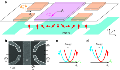
Figure 1 illustrates our proposed spin field effect transistor (FET) and its operating principle. An InGaAs heterostructure (see Methods Summary), one of the strong contenders to replace Si in future generations of large-scale integrated circuits (see International Technology Roadmap for Semiconductors; http://public.itrs.net), is used to provide a two-dimensional electron gas (2DEG) channel for ballistic electron transport under a metallic middle gate and between two gate-defined quantum point contacts (QPCs). The QPCs are narrow and short one-dimensional (1D) constrictions, usually formed by applying voltages to split gates patterned on the surface of a semiconductor heterostructure. Although the geometry is extremely simple, the QPC contains rich physicsthomas_prl96 ; bauer_nature13 ; iqbal_nature13 and has been suggested to generate a completely spin-polarized current due to SO coupling and/or electron-electron interactiondebray_naturenano09 ; wan_prb09 ; quay_naturephys10 ; nowak_apl13 ; chen_apl08 ; chen_prl12 .
In this all-electric spin FET, the left (right) QPC acts as a spin injector (detector) with nearly efficiency. To utilize the QPCs as spin injectors/detectors, we set a difference between the voltages on either side of the split gate (i.e. where and are the voltages applied respectively to the gate L1 and L2 in Fig. 1a, b) to generate a lateral inversion asymmetry and consequently a lateral SO effective magnetic field, , on electrons moving within the 1D constriction. The orientation of is along the axis, perpendicular to the lateral electric field and the electron momentum direction. Such a lateral SO coupling lifts the spin degeneracy and results in two spin-polarized 1D subbands shifted in wavevector as shown in Fig. 1c. In the case where the Fermi energy is tuned below the crossing point between two spin-polarized subbands, the left- and right-moving 1D electrons are both fully spin-polarizedmoroz_prb99 in the positive and negative -direction, respectively (hereafter, we refer to these subbands as the spin-up and spin-down states), thereby allowing the QPC to act as a spin injector/detector. Recent studiesdebray_naturenano09 ; wan_prb09 have further suggested that this lateral SO-induced spin splitting could be greatly enhanced by the strong electron-electron interaction in 1D systems (Fig. 1d), making the QPC spin injector/detector more reliable (see Supplementary Section 1). This method of spin injection circumvents many of the technical problems faced by ferromagnetic or optical alternatives (such as low spin-injection efficiencyschmidt_prb00 and scalability), and is compatible with the current manufacturing technology of FETs.
The spins supplied from the QPC injector remain ballistic and experience a SO effective magnetic field, , in the 2DEG channel due to the structural inversion asymmetry of the quantum well, which can be further controlled by changing the voltage applied to the middle gate (). In this transport channel the orientation of is parallel to the axis, and therefore perpendicular to the SO field in the QPC injector. This causes the injected spins to precess during transport between the QPCs (Fig. 1a). By modifying the gate voltage to vary , one can control the spin orientation of electrons travelling along the channel. The charge current is therefore modulated by the spin precession angle: electrons can pass through the QPC detector if their spin rotates to become parallel to the polarization direction, and cannot if their spin is anti-parallel. This gives rise to an oscillatory on/off switching with respect to gate voltage .
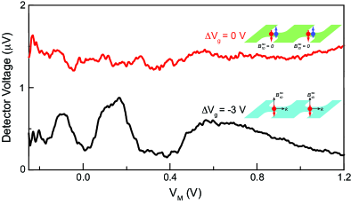
We demonstrate the operation of our spin FET in Fig. 2. Here, in order to simultaneously measure the on/off switching functionality and have precise control of the conductance of the QPCs, we configured the QPC detector as a voltage probe and measured the voltage across it. This voltage corresponds to the current flowing directly from the injector into the detector (see Methods Summary), i.e., the switching current in the spin FET. The conductance values of both QPCs are just above the threshold for conduction set at (where is the electron charge), at which the Fermi level is slightly above the very bottom of the spin-polarized 1D subbands to generate a spin polarized current in the presence of . When both QPCs are brought into the spin-polarized state by electrically introducing a lateral inversion asymmetry (black trace; V where and are the split gate voltages), an oscillatory on/off switching with variation as high as is observed as a function of . Such a large oscillating change in the conductance modulation (due to and spin precession) is about times greater than that observed in a conventional 2D spin FET designkoo_science09 which suffers from low signal levels as a result of the limited spin-injection efficiency, the short spin lifetime, and the spread of spin precession angles.
The voltage oscillation disappears when the lateral inversion asymmetry is removed from the QPCs by setting (red trace in Fig. 2). Spins injected from the QPC are no longer polarized along the axis as , and thus no oscillations in current are detected. It is worth noting that the experimental results presented here, in addition to showing the realization of spin FETs, provide the first direct evidence of spin polarization of QPCs at zero external magnetic field.
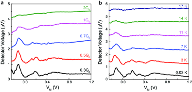
Figure 3a shows the oscillating voltages when the injector and detector QPCs are set at various conductance values. In a simple model of 1D transport with SO coupling (Fig. 1c), the right-moving electrons (with wavevectors) are fully spin-polarized at low conductance values when only the lowest spin-down subband is occupied. With increasing , the 1D subbands of both spin species become populated by electrons and the spin polarization decreases. Fig. 3a shows that the oscillation amplitude decreases with increasing , which is consistent with this model.
The influence of temperature on the oscillating voltage was also investigated (Fig. 3b). Since momentum scattering plays a key role in randomizing the spin precessiondyakonov_jetp71 ; dyakonov_sps86 ; elliott_pr54 , in a collision-free regime the spin relaxation may be negligible. The use of QPCs in the spin FET device allows only the ballistic transport electrons that directly moves from the injector to the collector to contribute to the signal, thereby implying that the observed decrease of the oscillation amplitude mainly results from the thermal reduction of the QPC polarization efficiency rather than the spin relaxation during transport. It suggests that much higher working temperature of the spin FET could be achieved in the presence of a larger 1D spin splitting, perhaps using wet-etched QPCsdebray_naturenano09 or InAs nanowires.
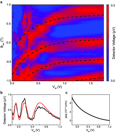
Finally, we demonstrate simultaneous electrical and magnetic control of spin precession. Earlier studies have shown that the spin precession can be driven either by the electric-field-tunable Rashba fieldkoo_science09 or by an external magnetic fieldcrooker_science05 ; appelbaum_nature07 ; lou_np07 . Here, the device allows us to combine these two controls. The Larmor frequency for a combined field is given by , which determines the spin precession angledatta_apl90 ; serra_prb05 (Supplementary Section 3):
| (1) |
where parameterizes the strength of Rashba SO coupling in the 2DEG channel, is the Landé -factor, is the Bohr magneton, is the electron effective mass, and is the length between the QPC injector and detector.
Figure 4a maps the spin precession angle, manifested in the voltage oscillation, as a function of (which controls and thus in Eq. 1) and . The external field was applied parallel to , both along the axis. The experimental results reveal the interplay of the electric and magnetic fields on spin precession, showing voltage oscillations along both and axes. The dashed lines simulate the shift in the peak positions of the voltage oscillation under this interplay using Eq. 1, with the parameters m, (where is the free electron mass), m-1 (estimated from the carrier density), in InGaAssimmonds_apl08 , and (see below). A good quantitative agreement was obtained between the experimental result and the theory.
The electric contribution to the spin precession angle, , and consequently the variation of the SO coupling constant with respect to the gate voltage, , can be estimated with a spline fitting procedure drawn through the peak and dip positions of the voltage oscillation. The fit for the spin precession angle, which manifests itself as an oscillatory voltage with a constant amplitude, and the estimated gate-dependent variation of the SO coupling constant are shown in Fig. 4b & c. Although the geometry of the device prevents us from directly measuring the local variation of under the middle gate, the relation obtained through the fit is consistent with previous work using Shubnikov-de Haas measurementsnitta_prl97 ; koo_science09 .
A quasi-1D spin FET is anticipated to have better performance than its 2D alternatives because the current modulation due to spin precession in 2D transport is expected to be washed out by the spread of precession anglesdatta_apl90 ; sugahara_ieee10 . This is because carriers with different injection angles travel different distances between the source and drain electrodes, thereby gaining a variety of spin precession angles when they reach the drain. The QPCs—in addition to providing spin selection with nearly efficiency and allowing only ballistic transport electrons to be collected (to sidestep the obstacles of low injection efficiency and spin relaxation)—define a quasi-1D path between the injector and detector to eliminate the phase spread, which results in a large oscillating signal modulation in the spin FET. On the basis of device functionality and application aspects, this all-semiconductor and all-electric spin FET offers a viable route for spin information processing.
Methods Summary
The devices were fabricated on an In0.75Ga0.25As/In0.75Al0.25As modulation-doped heterostructure (Supplementary Section 4). In reverse order of growth, the layer structure is as follows: 2 nm In0.75Ga0.25As (cap); 45 nm In0.75Al0.25As; 15 nm In0.75Al0.25As (Si doped); 60 nm In0.75Al0.25As (spacer); 30 nm In0.75Ga0.25As (quantum well); and 250 nm In0.75Al0.25As. The low-temperature carrier density and mobility of the 2DEG were measured to be cm-2 and cm2V-1s-1, respectively, giving a mean free path for momentum relaxation of m. An insulating layer (27 nm) of SiO2 was deposited on the surface of the wafer by plasma-enhanced chemical vapor deposition (PECVD). Following this, optically-defined Ti/Au surface gates were fabricated using standard optical lithography, to form bond pads. The surface gates with fine features were defined using electron-beam lithography. Measurements were performed in a dilution refrigerator, in which the devices were cooled down with a V bias on the surface gates to suppress random telegraph noise.
Figure 1b shows the scanning electron micrograph and circuit schematic of the spin FET device. In order to measure the conductances of both QPCs and the spin FET switching signal simultaneously, lock-in measurements were performed by applying two independent sources of (i) an a.c. voltage bias V at Hz to the QPC injector and (ii) an a.c. current bias nA at Hz to the QPC detector. Since the QPC detector was configured as a voltage probe, a voltage develops across the QPC detector in response to the Hz a.c. current injected ballistically into and through the detector: , where accounts for the transmission losses during transport in the semiconductor 2D channel (e.g. due to scattering; ), is the current emitted from the QPC injector, and is the spin-dependent transmission of the QPC detector. For clarity, the detector voltage presented here was normalized for a constant current from the injector nA.
Acknowledgements
We thank C.-W. Chang, C.-C. Cheng, M. Fletcher, S. N. Holmes, C.-T. Liang, S.-T. Lo and J. R. Petta for discussion and/or technical assistance on device fabrication and measurements. This work was supported by the Ministry of Science and Technology (Taiwan), the Headquarters of University Advancement at the National Cheng Kung University, and the Engineering and Physical Sciences Research Council (UK).
Author Contributions
P.C. and S.-C.H. performed the measurements and analysed the data, in which T.-M.C. participated. L.W.S. fabricated the devices with contributions from F.S, M.P., and T.-M.C; I.F., H.E.B., and D.A.R. provided wafers; J.P.G. and G.A.C.J. performed electron-beam lithography; C.H.C. and J.C.F. contributed some measurements. T.-M.C. wrote the paper with input from S.-C.H., L.W.S., F.S., and M.P.; T.-M.C. designed and coordinated the project.
References
- (1) Datta, S. & Das, B. Electronic analog of the electro-optic modulator. Appl. Phys. Lett. 56, 665-667 (1990).
- (2) Zutic, I., Fabian, J. & Das Sarma, S. Spintronics: Fundamentals and applications.Rev. Mod. Phys. 76, 323-410 (2004).
- (3) Awschalom, D. D. & M. E. Flatté, M. E. Challenges for semiconductor spintronics. Nat. Phys. 3, 153-159 (2007).
- (4) Crooker, S. A. et al. Imaging spin transport in lateral ferromagnet/semiconductor structures. Science 309, 2191-2195 (2005).
- (5) Appelbaum, I., Huang, B. & Monsma, D. J. Electronic measurement and control of spin transport in silicon. Nature 447, 295-298 (2007).
- (6) Lou, X. et al. Electrical detection of spin transport in lateral ferromagnet-semiconductor devices. Nat. Phys. 3, 197-202 (2007).
- (7) Koo, H. C. et al. Control of spin precession in a spin-injected field effect transistor. Science 325, 1515-1518 (2009).
- (8) Kum, H., Heo, J., Jahangir, S., Banerjee, A., Guo, W. & Bhattacharya, P. Room temperature single GaN nanowire spin valves with FeCo/MgO tunnel contacts . Appl. Phys. Lett. 100, 182407 (2012).
- (9) Schmidt, G., Ferrand, D., Molenkamp, L. W., Filip, A. T. & van Wees, B. J. Fundamental obstacle for electrical spin injection from a ferromagnetic metal into a diffusive semiconductor. Phys. Rev. B 62, R4790 (2000).
- (10) Wunderlich, J. et al. Spin Hall effect transistor. Science 330 1801-1804 (2010).
- (11) Betthausen, C. et al. Spin-transistor action via tunable Landau-Zener transitions. Science 337 324-327 (2012).
- (12) Rashba, E. I. Properties of semiconductors with an extremum loop I. Cyclotron and combinational resonance in a magnetic field perpendicular to the plane of the loop. Sov. Phys.: Solid State 2, 1109-1122 (1960).
- (13) Bychkov, Y. A. & Rashba, E. I. Oscillatory effects and the magnetic susceptibility of carriers in inversion layers. J. Phys. C 17, 6039-6045 (1984).
- (14) Nitta, J., Akazaki, T., Takayanagi, H. & Enoki, T. Gate control of spin-orbit interaction in an inverted In0.53Ga0.47AS/In0.52Al0.48AS heterostructure. Phys. Rev. Lett. 78, 1335-1338 (1997).
- (15) Koga, T., Nitta, J., Akazaki, T. & Takayanagi, H. Rashba spin-orbit coupling probed by the weak antilocalization analysis in InAlAs/InGaAs/InAlAs quantum wells as a function of quantum well asymmetry. Phys. Rev. Lett. 89, 046801 (2002).
- (16) Thomas, K. J. et al. Possible spin polarization in a one-dimensional electron gas. Phys. Rev. Lett. 77, 135-138 (1996).
- (17) Bauer, F. et al. Microscopic origin of the ‘0.7-anomaly’ in quantum point contacts. Nature 501, 73-78 (2013).
- (18) Iqbal, M. J. et al. Odd and even Kondo effects from emergent localization in quantum point contacts. Nature 501, 79-83 (2013).
- (19) Debray, P. et al. All-electric quantum point contact spin-polarizer. Nature Nanotechnology 4, 759-764 (2009).
- (20) Wan, J., Cahay, M., Debray, P. & Newrock, R. Possible origin of the 0.5 plateau in the ballistic conductance of quantum point contacts. Phys. Rev. B 80, 155440 (2009).
- (21) Quay, C. H. L. et al. Observation of a one-dimensional spin-orbit gap in a quantum wire. Nature Physics 6, 336-339 (2010).
- (22) Nowak, M. P. & Szafran, B. Spin current source based on a quantum point contact with local spin-orbit interaction. Appl. Phys. Lett. 103, 202404 (2013).
- (23) Chen, T. M., Graham, A. C., Pepper, M., Farrer, I. & Ritchie, D. A. Bias-controlled spin polarization in quantum wires. Appl. Phys. Lett. 93, 032102 (2008).
- (24) Chen, T. M., Pepper, M., Farrer, I., Jones, G. A. C. & Ritchie, D. A. All-electrical injection and detection of a spin-polarized current using 1D conductors. Phys. Rev. Lett. 109, 177202 (2012).
- (25) Moroz, A. V. & Barnes, C. H. W. Effect of the spin-orbit interaction on the band structure and conductance of quasi-one-dimensional systems. Phys. Rev. B 60, 14272 (1999).
- (26) D’yakonov, M. I. & Perel’, V. I. On spin orientation of electrons in interband absorption of light in semiconductors. Zh. Eksp. Teor. Fiz. 60, 1954-1965 (1971) [Sov. Phys. JETP 33, 1053 (1971)].
- (27) D’yakonov, M. I. & Kachorovskii, V. Y. Spin relaxation of two-dimensional electrons in noncentrosymetric semiconductors. Sov. Phys. Semicond. 20, 110-112 (1986).
- (28) Elliott, R. J. Theory of the effect of spin-orbit coupling on magnetic resonance in some semiconductors. Phys. Rev. 96, 266-279 (1954).
- (29) Serra, L., Sánchez, D. & López, R. Rashba interaction in quantum wires with in-plane magnetic fields. Phys. Rev. B 72, 235309 (2005).
- (30) Simmonds, P. J. et al. Quantum transport in In0.75Ga0.25As quantum wires. Appl. Phys. Lett. 92, 152108 (2008).
- (31) Sugahara, S. & Nitta, J. Spin-Transistor Electronics: An Overview and Outlook. Proceedings of the IEEE 98, 2124-2154 (2010).