Electrically tunable spin polarization of chiral edge modes in a quantum anomalous Hall insulator
Abstract
In the quantum anomalous Hall effect, chiral edge modes are expected to conduct spin polarized current without dissipation and thus hold great promise for future electronics and spintronics with low energy consumption. However, spin polarization of chiral edge modes has never been established in experiments. In this work, we theoretically study spin polarization of chiral edge modes in the quantum anomalous Hall effect, based on both the effective model and more realistic tight-binding model constructed from the first principles calculations. We find that spin polarization can be manipulated by tuning either a local gate voltage or the Fermi energy. We also propose to extract spin information of chiral edge modes by contacting the quantum anomalous Hall insulator to a ferromagnetic (FM) lead. The establishment of spin polarization of chiral edge modes, as well as the manipulation and detection in a fully electrical manner, will pave the way to the applications of the quantum anomalous Hall effect in spintronics.
pacs:
73.20.-r, 72.25.-b, 85.75.-dIntroduction - For a two dimensional electron gas under a strong magnetic field, Landau levels are formed and drive the system into a state characterized by the zero longitudinal resistance and the quantized Hall conductance with an integer value of . This phenomenon is known as the quantum Hall (QH) effect, which was discovered by Von. Klitzing in 1980 Klitzing et al. (1980). Recently, it was theoretically predicted Haldane (1988); Liu et al. (2008); Yu et al. (2010) that this type of quantization in the Hall conductance can also be realized in magnetic insulating materials at a zero external magnetic field. This phenomenon, dubbed as the “quantum anomalous Hall (QAH) effect”, was soon observed experimentally in magnetically doped topological insulators (TIs), the Cr or V doped (Bi,Sb)2Te3 films Chang et al. (2013); Kou et al. (2014); Checkelsky et al. (2014); Bestwick et al. (2015); Chang et al. (2015). The physical origin of the QAH effect is spin-orbit coupling and exchange coupling between magnetic moments and electron spins in magnetic materials, rather than magnetic fields and the associated Landau levels Haldane (1988). The experimental observation of the exact quantization of Hall conductance and neglegible longitudinal resistance confirm the dissipationless nature of transport for the QAH effect Bestwick et al. (2015); Chang et al. (2015) and the mapping of global phase diagram establishes the topological equivalence between the QH effect and the QAH effect Checkelsky et al. (2014); Kou et al. (2015).
Similar to the case of the QH effect, dissipationless currents in the QAH insulators are carried by one dimensional (1D) chiral edge modes (CEMs), which propagate along one direction at the edge of the system and are robust against disorder scatterings. CEMs are believed to hold great promise for the potential applications in electronics and spintronics with low power consumption Zhang and Zhang (2012). For any spintronic application, it is required for CEMs to carry spin polarization (SP). Naively, one may expect that SP of CEMs should exist and follows bulk magnetization, but this issue has seldom been studied theoretically. In Ref. Wu et al. (2014), SP of CEMs was studied in the context of a two band model, which is more relevant to cold atom systems. For condensed matter systems, it is more complicated since spin and orbital are mixed with each other due to spin-orbit coupling sup .
In this letter, we investigate SP of CEMs of the QAH effect in magnetically doped (Bi,Sb)2Te3. Surprisingly, we find that SP of CEMs though exists but does not follow bulk magnetization, and sensitively depends on the boundary conditions. In particular, we find that the direction of SP of CEMs can be manipulated by a local gate voltage, thus opening the possibility of controlling SP of CEMs in a fully electrical manner. We provide a simple physical picture of SP of CEMs based on the effective four-band model and further study its behavior in the more realistic calculations based on the tight-binding model constructed by the Wannier function method of the first principles calculations Marzari and Vanderbilt (1997); Souza et al. (2001). We propose the spin valve effect Dieny (1994) of CEMs in a standard experimental setup of the Hall measurement with ferromagnetic (FM) leads to extract spin information of CEMs.
Spin polarization of chiral edge modes - To study SP of CEMs in a QAH insulator, we first consider an effective four band model for magnetically doped (Bi,Sb)2Te3 films Yu et al. (2010). The low energy physics of this system is dominated by two surface states from top and bottom surfaces, which hybridize with each other to open a gap due to the finite size effect. Meanwhile, the exchange coupling of electron spin arises from the doping of magnetic atoms. Thus, the effective Hamiltonian is given by
| (1) | |||||
where and matrices are Pauli matrices of spin and layer (top or bottom) degree of freedom, and . gives hybridization between the top and bottom surface states. The term describes exchange coupling between electron spin and magnetization of magnetic doping. We only consider the out-of-plane magnetization . is a higher order correction of the surface states and is defined as the strength of hexagon warping effect Liu et al. (2010); Fu (2009). The term denotes the asymmetric potential between the top and bottom layers which has spatial dependence and can be induced by a global or local gate voltage.
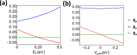
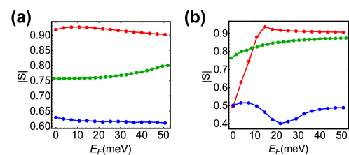
The edge spectrum of our effective model, as well as the corresponding SP, can be evaluated with the help of the iterative Green’s function method Sancho et al. (1984, 1985). We consider a semi-infinite system with the direction still translationally invariant and one edge parallel to direction (x-edge). The following set of parameters, , is chosen to keep the system in the QAH regime. The local Green’s function on the x-edge can be evaluated iteratively. The total local density of states (DOS) and the spin DOS along the th direction () are defined as and , respectively. As shown in the Supplementary Materials sup , the CEM can be easily identified from the peak of local DOS on the x-edge. The corresponding SP along the th direction () for the CEM is normalized by the total DOS as . In Fig. 1 (a) and (b), the SP of the CEMs is plotted for all three spin components with different local gate voltages and chemical potentials. Let us take the lattice constant to be unity and label the lattice site with an integer index , with being the distance between the th lattice site and the boundary. Here the local gate voltage is added only on all lattice sites, which leaves the bulk states unchanged. We find that for a zero gate voltage (), only the component () SP of CEMs is non-zero. If we apply a local gate voltage, SP becomes non-zero for both the and direction, but still keeps zero for the direction. Therefore, SP of CEMs can exist within the - plane and can be controlled by a local gate voltage. It is also interesting to notice that the local gate voltage mainly controls the amplitude of , but barely change that of (see Fig. 1(b))sup . The chemical potential can also tune the magnitude of (both and ) at a zero (finite) local gate voltage, as shown in Fig. 1 (a). Therefore, our effective model (Eq. 1) suggests that SP of CEMs can be manipulated by either applying a local gate voltage or tuning the chemical potential.
Next we provide an analytical solution of the eigen wave function for the Hamiltonian (Eq. 1) with to understand the electrical tunability of SP of CEMs. Assume , the system will enter QAHE regime when . The zero mode of the Hamiltonian localizing on the edge can be solved exactly sup as
| (2) |
where is a normalization factor and . Here denote spin up (down) state along the direction, and denotes the contribution from the top (bottom) layer of thin films. The wave function (2) of CEMs consists of two parts: one part on the top surface with SP along the direction and the other on the bottom surface with SP along the direction. Thus, the SP is locked to the layer (top or bottom) for the CEMs. A local gate voltage can push the wave functions of CEMs into one layer, thus leading to the change of SP.
The above analysis of SP of CEMs is based on the effective four-band model (Eq. 1) and one may ask if these results still hold for a realistic system, such as Cr or V doped (Bi,Sb)2Te3. To answer this question, we carry out explicit calculations for a magnetically doped Sb2Te3 thin film system with the realistic tight-binding model constructed from the maximal localized Wannier function (MLWF) method Marzari and Vanderbilt (1997); Souza et al. (2001) based on the first principles calculations, which has been successfully applied to the quantitative study of the QAH effect in magnetically doped (Bi,Sb)2Te3 Wang et al. (2013a, b). The exchange coupling between electron spin and magnetization is included in the tight-binding model in the mean field approximation . Here we consider only the contribution from out-of-plane magnetization and is the z directional spin operator for Sb (Te) atoms. In our calculation, we consider a film with two quintuple layers and choose the exchange coupling strength to be eV and eV, which is strong enough to drive the system into the QAH phase. The edge dispersion is also calculated with the iterative Green function method in a semi-infinite configuration along (100) direction, as shown in Fig. 2 (a). For edge modes, we find three left movers (the modes I, II and IV) and two right movers (the modes III and V), suggesting that one chiral edge mode (left mover) and the other two trivial 1D edge modes (or non-chiral edge modes) Wang et al. (2013a). Since the mode IV is directly connected to V, these two modes must be trivial 1D edge modes and thus we focus on the modes I, II and III below. The influence of the local gate voltage ( eV) is shown in Fig. 2 (b), from which one can see that the number of left and right movers is unchanged, but their energy dispersions are shifted.
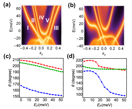
After obtaining the edge state Green function, it is straightforward to calculate the corresponding SP vector . First of all, is vanishingly small compared to other spin components. This confirms the results from the effective four band model. Thus, only appears in the - plane and can be characterized by its magnitude and a polarization angle relative to axis. For , we notice that it vanishes at for the effective four band model, while it is non-zero in the realistic tight-binding model. This difference is because of the out-of-plane mirror symmetry in our four band model, which is absent in realistic crystals. Therefore, both and are non-zero even at in realistic tight-binding model. We plot Fermi energy dependence of polarization angle at the local gate eV and eV in Fig. 2 (c) and (d). The polarization angles for the modes I (red lines) and III (green lines) behave similarly to each other, while that of the mode II (blue lines) reveals a completely different characteristics. This is a clear evidence that the modes I and III are connected to each other, forming a non-chiral edge mode, while the mode II can be identified as the non-trivial CEM. In Fig. 2 (d), we notice an abrupt change of polarization angle for the modes I and II when is between 0 meV and 20 meV. Compared with the energy dispersion in Fig. 2 (b), we find that this change results from the strong hybridization effect between the modes I and II. Thus, the CEM and non-chiral mode are not well defined in this regime. In the other regime, we find a smooth change of SPs with respect to local gate voltages and chemical potentials.
Experimental detection of edge spin polarization - Our theoretical calculations based on both the effective model and realistic tight-binding model have clearly demonstrate electrically tunable SP in magnetically doped (Bi,Sb)2Te3. However, the experimental detection of SP is not an easy task since the bulk is FM and it is unclear how to distinguish SP of CEMs from that of bulk ferromagnetism by magnetization measurement. In contrast, when the Fermi energy is tuned into the bulk gap, the transport signals are dominated by CEMs. Thus, it is more promising to search for SP of CEMs from transport measurements.
Our proposal is based on a four terminal device with a FM probe as the fourth probe, as shown in Fig. 3 (a). This experimental setup is similar to that in the study of disordered leads in the QH system and here FM leads play the role of disordered leads Datta (1997). When SP of the CEM is parallel to magnetization of the FM lead, it can flow into the lead, while when they are opposite, it will be scattered. We apply a voltage drop between the leads and ( and ) and also introduce a split gate, denoted as SG in the Fig.3 (a). Due to the split gate, there are two types of currents flowing from the lead to : the current , which goes through , and the current flowing directly from to . Based on the Landauer-Bttiker formula Büttiker (1986, 1988), the current to the lead shares the same chemical potential as , while the current is determined by the chemical potential in the lead . Importantly, we assume that chemical potentials of two currents and have not reached equilibrium when they enter the FM lead. This is determined by the inelastic scattering length, which is estimated as several for the QH case Koch et al. (1991), and we expect a similar length scale in our case. Thus, the corresponding SPs are also expected to be different for these two currents. Since the scattering rate into the FM lead depends on the relative angle between the SP of CEMs and . We expect the transmissions of and also depend on of the FM lead. As a result, the chemical potential in will vary when rotating . This provides a detectable signal, which is similar to the spin valve effect Dieny (1994), in transport measurements and can be directly related to SP of CEMs. It should be emphasized that the split gate SG plays an essential role here. Without the split gate, all currents flowing into come from , and thus the corresponding chemical potential in must be equal to that of , independent of magnetization direction of the FM lead.

To formulate this idea, we assume that only p () fraction of the net edge current can flow from to due to the split gate, as shown in Fig. 2 (a), so . We further assume the () fraction of the current () has spin polarizing along . Since SP of CEMs depends on chemical potential, it is reasonable to assume . Therefore, the currents from () to are and , respectively, as shown in Fig. 3 (a). The Hall conductance can be derived based on Landauer-Bttiker formula sup as
| (3) |
with the conductance quanta . From Eq. (3), one can see that when there is no split gate (), , which recovers the quantized Hall conductance and is independent of its spin information. When a split gate is introduced, and , and will deviate from the quantized value and we discuss how to extract the information of SP of CEMs from the Hall resistance measurement in the Supplementary Materials sup .
For the realistic systems of magnetically doped (Bi,Sb)2Te3, we have shown additional non-chiral modes coexisting with CEMs. Thus, it is natural to ask how these non-chiral modes influence the above transport measurement. We consider one pair of non-chiral edge mode (mode I and III in Fig. 2 (a)) and one CEM (mode II) and further assume no inter-channel scattering between different modes for simplicity. We take the modes I and II flowing clockwise (as shown in Fig. 3 (a)), and the mode III flowing counter-clockwise (flipping the directions of currents in Fig. 3 (a)). () is defined as the transmission into FM probe of edge current () for the modes I,II and III, with and . The explicit expression of transverse resistance is shown in the Supplementary Materials sup . In the limit where the split gate vanishes (), the transverse conductance becomes
| (4) |
which deviates from the quantized value. Thus, in contrast to the single CME case, Hall resistance will depend on the magnetization direction of FM leads even without any split gate for the case with both CME and non-chiral modes.
To apply Eq. (4) to magnetically doped Sb2Te3 films, we need to extract the coefficients s from our realistic tight-binding model. As discussed above, s are determined by the projection of SP of CEMs into the magnetization direction of FM leads. Since SP of CEMs only exists in the - plane, we only concern the projection of SP into the - plane. Let’s assume has an angle relative to direction in the - plane, as shown in Fig. 3 (b). The corresponding projection operator for CEMs is defined as:
| (5) |
Consequently, the angle dependent transmission for the th edge mode is given by
| (6) |
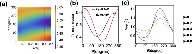
where is the wave function for the mode . With Eq. 4 and Eq. 6, we can calculate the transmissions s for the modes I, II and III as a function of and Fermi energy for the local gate voltage for our realistic tight-binding model sup . For the chemical potential meV, dependence of transmission s and the Hall resistance , are shown in Fig. 3 (c) and (d), respectively. shows a strong dependence on , thus revealing the spin valve effect for CEMs Dieny (1994). This provides a very clear and experimentally feasible evidence to detect spin signal in a QAH insulator.
Discussions - In summary, we have shown that SP of CEMs can be generated, manipulated and detected in a QAH insulator in a fully electric manner. This paves the way of potential applications for the QAH effect in spintronics. Disorder is inevitable in realistic samples and we show the stability of SP of CEMs against disorder in the Supplementary Materials sup . Although we focus on the magnetically doped (Bi,Sb)2Te3 films here, the electric controllability of SP of CEMs is a general property of a QAH insulator. The bulk topology (non-zero Chern number) only guarantees the existence of CEMs, but the detailed form of wave functions of CEMs depends on local electric environment, and thus can be controlled by a local gate voltage. We expect a similar effect also occurs in other QAH insulators, such as Mn doped HgTe quantum wells Liu et al. (2008) and InAs/GaSb quantum wells Wang et al. (2014), where the local gate voltage can induce a local Rashba spin-orbit coupling and tilt SP of CEMs.
Acknowledgement - We would like to acknowledge Cui-Zu Chang, Moses Chan, Abhinav Kandal, Jainendra Jain, Jagadeesh Moodera, Xiao-Liang Qi and Nitin Samarth for the helpful discussions.
References
- Klitzing et al. (1980) K. v. Klitzing, G. Dorda, and M. Pepper, Physical Review Letters 45, 494 (1980).
- Haldane (1988) F. D. M. Haldane, Physical Review Letters 61, 2015 (1988).
- Liu et al. (2008) C.-X. Liu, X.-L. Qi, X. Dai, Z. Fang, and S.-C. Zhang, Physical review letters 101, 146802 (2008).
- Yu et al. (2010) R. Yu, W. Zhang, H.-J. Zhang, S.-C. Zhang, X. Dai, and Z. Fang, Science 329, 61 (2010).
- Chang et al. (2013) C.-Z. Chang, J. Zhang, X. Feng, J. Shen, Z. Zhang, M. Guo, K. Li, Y. Ou, P. Wei, L.-L. Wang, et al., Science 340, 167 (2013).
- Kou et al. (2014) X. Kou, S.-T. Guo, Y. Fan, L. Pan, M. Lang, Y. Jiang, Q. Shao, T. Nie, K. Murata, J. Tang, et al., Physical review letters 113, 137201 (2014).
- Checkelsky et al. (2014) J. Checkelsky, R. Yoshimi, A. Tsukazaki, K. Takahashi, Y. Kozuka, J. Falson, M. Kawasaki, and Y. Tokura, Nature Physics 10, 731 (2014).
- Bestwick et al. (2015) A. Bestwick, E. Fox, X. Kou, L. Pan, K. L. Wang, and D. Goldhaber-Gordon, Physical review letters 114, 187201 (2015).
- Chang et al. (2015) C.-Z. Chang, W. Zhao, D. Y. Kim, H. Zhang, B. A. Assaf, D. Heiman, S.-C. Zhang, C. Liu, M. H. Chan, and J. S. Moodera, Nature materials 14, 473 (2015).
- Kou et al. (2015) X. Kou, L. Pan, J. Wang, Y. Fan, E. S. Choi, W.-L. Lee, T. Nie, K. Murata, Q. Shao, S.-C. Zhang, et al., arXiv preprint arXiv:1503.04150 (2015).
- Zhang and Zhang (2012) X. Zhang and S.-C. Zhang, in SPIE Defense, Security, and Sensing (International Society for Optics and Photonics, 2012) pp. 837309–837309.
- Wu et al. (2014) J. Wu, J. Liu, and X.-J. Liu, Physical review letters 113, 136403 (2014).
- (13) See Supplementary Materials for details .
- Marzari and Vanderbilt (1997) N. Marzari and D. Vanderbilt, Physical review B 56, 12847 (1997).
- Souza et al. (2001) I. Souza, N. Marzari, and D. Vanderbilt, Physical Review B 65, 035109 (2001).
- Dieny (1994) B. Dieny, Journal of Magnetism and Magnetic Materials 136, 335 (1994).
- Liu et al. (2010) C.-X. Liu, X.-L. Qi, H. Zhang, X. Dai, Z. Fang, and S.-C. Zhang, Physical Review B 82, 045122 (2010).
- Fu (2009) L. Fu, Physical review letters 103, 266801 (2009).
- Sancho et al. (1984) M. L. Sancho, J. L. Sancho, and J. Rubio, Journal of Physics F: Metal Physics 14, 1205 (1984).
- Sancho et al. (1985) M. L. Sancho, J. L. Sancho, J. L. Sancho, and J. Rubio, Journal of Physics F: Metal Physics 15, 851 (1985).
- Wang et al. (2013a) J. Wang, B. Lian, H. Zhang, and S.-C. Zhang, Physical review letters 111, 086803 (2013a).
- Wang et al. (2013b) J. Wang, B. Lian, H. Zhang, Y. Xu, and S.-C. Zhang, Physical review letters 111, 136801 (2013b).
- Datta (1997) S. Datta, Electronic transport in mesoscopic systems (Cambridge university press, 1997).
- Büttiker (1986) M. Büttiker, Physical Review Letters 57, 1761 (1986).
- Büttiker (1988) M. Büttiker, Physical Review B 38, 9375 (1988).
- Koch et al. (1991) S. Koch, R. Haug, K. v. Klitzing, and K. Ploog, Physical review letters 67, 883 (1991).
- Wang et al. (2014) Q.-Z. Wang, X. Liu, H.-J. Zhang, N. Samarth, S.-C. Zhang, and C.-X. Liu, Physical review letters 113, 147201 (2014).
.1 Supplementary Materials for “Edge spin polarization in Quantum Anomalous Hall Insulators”
.2 Analytical solution of edge wave function in effective model
To solve for the zero mode wave function of the effective model, we can first apply a unitary transformation ,
leading to
We set and becomes block diagonal. We take and assume , and band inversion happens when . We would like to emphasize that the two-band model taken in Ref. Wu et al. (2014) is just one block of the above four-band Hamiltonian (.2). Nevertheless, the bases for the Hamiltonian (.2) are , where ”” denotes bonding/anti-bonding state between top and bottom surface states. The corresponding spin operators are given by
Thus, we find that the spin operators in the four band model are different from those used in the two-band model in Ref. Wu et al. (2014), which are more relevant to the cold atom system.
Now we consider the case with , in which the lower block of is in the QAH phase while the upper block is in the trivial phase. For the lower block, we have
We choose the following set of parameters which satisfies the above band inversion condition: .
The wave-function of zero energy mode of the chiral edge mode can be solved for the lower block Hamiltonian. Let us assume the edge is along the y direction, so we consider first, and check the eigen equation for zero mode
| (7) |
Multiply both sides by ,
| (8) |
Consider the ansatz , where , we have
| (9) |
Thus the wave function should be the following linear combination:
| (10) |
with
| (11) | |||||
Assuming the material (vacuum) region is at (), then we require that wave function vanishes at both and . This requires , and to be negative. So the wave function is given by
| (12) |
Notice that the spinor part is defined in the hybridized bases . Then can be written as
| (13) | |||||
We emphasize again that the above solution does not correspond to a net spin polarization along the y direction, as discussed in Ref. Wu et al. (2014), due to the different bases. The wave function of CEMs consists of two parts: one part on the top surface with SP along the direction and the other on the bottom surface with SP along the direction. These two contributions exactly cancel each other, leading to zero net SP of CEMs. From the symmetry perspective, we notice that there is an emergent mirror symmetry between the top and bottom surfaces, which requires . Therefore, applying a local gate voltage breaks this mirror symmetry and yields an imbalance of SP between the top and bottom surfaces, giving rise to a finite . The absence of is completely accidental, as a result of setting . Numerically, when assigning non-zero values to and , non-zero appears, as shown in Fig. [1] in the main text. Therefore, is insensitive to this mirror symmetry breaking, just as we have numerically verified. To conclude, applying a local gate voltage changes both magnitude and direction of CEM SP.
I Transverse conductance from Landauer-Bttiker formula
In this section, we will derive analytical expressions of transverse conductance based on Landauer-Bttiker formula Büttiker (1986, 1988). We will first discuss the situation with one single chiral edge mode, and then generalize the expression to a case where a chiral edge mode and one pair of non-chiral edge mode coexist.
Following the setup configuration in Fig. [3] (a) in the main text, the conductance matrix G for a single chiral edge state (flowing clockwise) is given by
where the bases for matrix G is (). Here is the split gate transmission, while and are transmissions into FM probe of currents from and . Here a matrix element describes the conductance contribution from probe to probe . Then, current voltage relations are
Here () denotes the current that flows into the th probe. Notice that and , giving rise to
| (14) |
The transverse conductance is given by
| (15) |
Numerically, we plot the dependence of transverse resistance in Fig. 4 (c). Here, we take current (from ) at eV and (from ) at eV. Transmission of and into is calculated in Fig. 4 (a), which will be discussed in details in a later section. In the Fig. 4 (b), we extract the transimission information for eV (blue line) and eV (red line) from Fig. 4 (a), which provides us with the and at different . Transmission into the split gate is chosen at various values. As long as the split gate structure exists (), there will be an obvious dependence of Hall resistance , as shown in Fig. 4 (c). But when the split gate structure is absent, transverse resistance will be quantized despite the value of .
For the magnetically doped Sb2Te3 QAH system, we consider two clock-wise modes (mode I and III) and one counter-clockwise mode (mode II). Let us define () to be the transmission into FM probe of edge current () for the modes I,II and III, with and . So the conductance matrix for mode I and mode II can simply take the form of Eq I, while conductance matrix for mode III is as follows:
The net conductance matrix is simply an addition of all three conductance matrix . After some calculations, we arrive at the following Hall conductance
| (16) |
In the limit where the split gate vanishes (), the transverse conductance becomes
| (17) |
II Electron current transmission at the ferromagnetic probe
In the previous discussion, we have shown that transverse conductance has a strong dependence on transmissions at the FM probe . In the main text, we have defined the transmission based on a projection operator approach. Since the edge state Green function can be calculated with the help of iterative Green function method, we can easily rewrite the transmission expression in terms of the edge state Green function for edge mode i (i=I,II,III)
| (18) |
Based on Eq. 18, in Fig. 4 (a), we calculate the chemical potential and dependence of transmission for the chiral edge state in the effective QAH model. Here we apply a local gate voltage eV. The blue line ( eV) and red line ( eV) denote two different chemical potentials due to the split gate effect. The two Fermi energies are the s we choose to calculate transverse resistance in Fig 4 (c). We further plot the transmissions at these two fixed Fermi energies in Fig. 4 (a).

For the magnetically doped Sb2Te3 QAH system, non-chiral edge modes show up and we consider the co-existence of a pair of non-chiral edge modes (mode I and mode III) and a chiral mode (mode II). Following a similar approach, we make use of the edge state Green function and plot chemical potential and dependence of transmissions s for all three modes in Fig.5 (a) to (c). Here the white dashed line shows the fixed chemical potential meV, which we picked to calculate in the main text. In Fig.5 (d), we compare the transmission of all three modes at the fixed Fermi energy meV. We notice that transmission of mode II peaks at around degree while that of mode I and III peaks at around degree. This means that transmission peaks happen at the polarization angle of these edge modes. The above results are consistent with the fact that FM probe is transparent to the electrons with spin parallel to the magnetization of the FM probe.
III Magnitude of edge spin polarization for magnetically doped Sb2Te3 QAH systems
We have found that for magnetically doped Sb2Te3 QAH systems, spin polarization is a two dimensional vector living in - plane, due to the absence of its component. Therefore, can be written in terms of polar coordinates . In the main text, we have plotted the polarization angle of mode I, II and III. It is shown that mode I (left mover) and mode III (right mover) share a very similar characteristics, and we claim that these two modes should be connected to each other and become trivialized. To make our results complete, here we show that magnitude plot of spin polarization in Fig. 6. Following the same color convention, of edge mode I, II and III are plotted in red, blue and green. In fact, the value of can be closely related to the calculation details. For example, when locating the CEMs in the iterative Green function (DOS) calculation, a small error in locating the peak position of DOS may lead to a different value of the corresponding CEM. Compared to , polarization angle is barely affected by such calculation error. Therefore, we would like to point out that polarization angle is more essential in our discussion here.
IV Decay length of chiral edge states
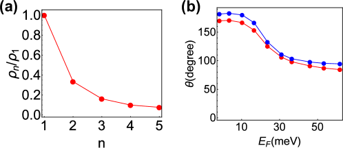
Let us denote the density of state calculated from the th lattice sites as , with . In Fig.7 (a), we have plotted the value of in units of of mode II in the Sb2Te3 based QAHE system. It clearly shows that the edge state is highly localized on the edge, and exponentially decays into the bulk. By doing an exponential fit, we find that the decay length is times lattice constant. In our calculation for SP, we have included the total contribution from all lattice sites, which we identify as the major contribution. In general one can integrate over the entire semi-infinite space, which is rather costly in calculation, while giving only a small modification to our present results. Actually, we can even show the SP angle is dominated by the contribution from the lattice sites. As shown in Fig. 7 (b), we calculated the SP angle of CEM (mode II) with eV for only , and plot evolving with Fermi energy (red line). In comparison, we also plot the SP angle calculated for all lattice sites with blue line. It is clear that the lattice sites give the major contributions to , while lattice sites together only give a rather small correction to . We also would like to emphasize that we are not interested the exact value of CEM SP, which depends on the details of samples in experiments. The essential physics here is that the CEM SP can be manipulated electrically, despite its exact value.
V Influence of FM probe on the QAHE

It is possible that attaching a FM gate to a QAH sample may change the QAH sample locally. For example, the value of CEM spin polarization may be affected in this regime. However, what is physically interesting is the tunability of spin polarization as a result of electrical approaches (chemical potential and local gate tuning). The exact value of CEM spin polarization is not that interesting to us. Therefore, we expect the angle-dependent transverse resistance should still be observed in this case.
In an extreme situation, QAH state is destroyed locally in the vicinity of FM probe, as shown in Fig. 8. In this case, one can simply treat this local part of QAH sample as an extension of the FM gate. Then a new boundary between FM probe (including its extension) and the QAH sample emerges and edge states still exist on this new boundary, as long as the rest of sample remains in the QAH phase. As a result, our physical picture of this transport experiment still holds.
VI Stability of edge spin polarization under disorder
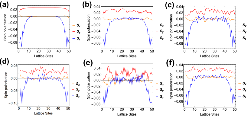
In this section, we show that the above spin polarization of QAH edge states in the simple effective model (Eq. [1] in the main text) is robust under disorder effect. We start from a finite size real space Green function with a lattice configuration with and . To discuss its chiral edge states, we perform iteration of Green function along the direction, so that system is finite along the direction while semi-infinite along direction. In this case, SDOS (spin polarization) of edge states on the -edge will be obtained. Disorder potentials are white-noise-like on-site potentials, and are included locally on the edge for simplicity. The magnitude of disorder potential is between and , where is the disorder strength. We also perform the configuration averaging, the number of which is defined as , for disorders.
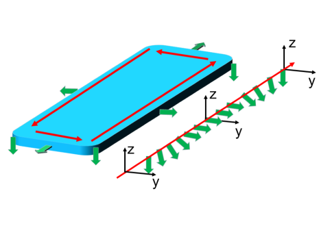
In Fig. 9 (a), we first calculate edge spin polarization without any disorder (). A finite local gate voltage ( eV) and a finite Fermi energy ( eV) are considered to guarantee non-zero spin polarization. The -axis represents lattice sites of the one-dimensional lattice chain on the -edge and -axis is for spin polarization. We can clearly see strong finite size effect on the 1D edge chain: At both ends of this 1D chain, there are abrupt changes of spin polarization in all three components. Such a finite size effect can be removed by imposing periodic boundary condition along direction, and resulting spin polarization is exactly shown in Fig. [1] (a) and (b) (in the main text). This means that for a finite size QAH sample, spin polarization of an electron on the -edge is along direction. As shown in Fig. 10, while approaching the sample corner between -edge and -edge, its spin polarization (green arrows) gradually becomes along direction. Finally, when this electron enters -edge, its spin polarization becomes along direction.
When disorder is introduced, we can see that the fluctuation of spin polarization increases as the disorder strength increases, as shown in Fig. 9 (b)-(e). But this disorder induced fluctuation decreases as we increases the configuration averaging number (Fig. 9 (f)). This concludes that spin polarization of chiral edge state in QAHE is robust against disorder effects.