Controlling a three dimensional electron slab of graded AlxGa1-xN
Abstract
Polarization induced degenerate -type doping with electron concentrations up to 1020 cm-3 is achieved in graded AlxGa1-xN layers (: 0%37%) grown on unintentionally doped and on -doped GaN:Si buffer/reservoir layers by metal organic vapor phase epitaxy. High resolution x-ray diffraction, transmission electron microscopy and electron energy loss spectroscopy confirm the gradient in the composition of the AlxGa1-xN layers, while magnetotransport studies reveal the formation of a three dimensional electron slab, whose conductivity can be adjusted through the GaN(:Si) buffer/reservoir.
I Introduction
The last two decades since the inception of the III-nitride based blue light emitting diodes (LEDs) Nakamura et al. (1993); Nakamura (1995), have witnessed the emergence of III-nitrides as prominent material systems in state-of-the-art semiconductor technology Gutt et al. (2012); Morkoç (2008). In particular, heterostructures based on AlxGa1-xN/GaN represent the building-blocks for a number of current (opto)electronic devices, including blue and white LEDs Gutt et al. (2012); Morkoç (2008), laser diodes and lasers Yoshida et al. (2008), high-power- Shur (1998); Yeluri et al. (2015) and high-electron-mobility-transistors (HEMTs) Mishra (2002); Sun et al. (2015). Beside the tunability of the bandgap from the 3.4 eV of GaN to the 6.2 eV in AlN at room temperature, there is between GaN and AlN a 2.5% lattice mismatch, allowing the pseudomorphic growth of AlxGa1-xN layers with a biaxial tensile strain on GaN. This leads to a compressive strain along the -axis of the wurtzite (wz) structure, which induces a macroscopic electric field. Additionally, due to the lack of inversion symmetry, wz-III-nitrides also have piezoelectric constants as large as 0.73 Cm-2-1.47 Cm-2 that exceed by over two orders of magnitude those of relevant zinc-blende semiconductors, whose values are in the range 0.01 Cm-2-0.1 Cm-2 [Bernardini et al., 1997a, b; Ambacher et al., 2002]. With ab initio calculations it was shown, that the macroscopic polarization in wurtzite nitrides is nonlinear Bernardini and Fiorentini (2001). While the nonlinearity of the spontaneous polarization depends on the microscopic structure of the alloy, the nonlinear piezoelectric polarization is a bulk effect. The presence of this large spontaneous and induced polarization in AlxGa1-xN/GaN heterostructures leads to the formation of a 2-dimensional electron gas (2DEG) with electron densities exceeding 1013 cm-2 [Smorchkova et al., 1999; Schmult et al., 2006; Hsu and Walukiewicz, 2001], even in the absence of nominal doping. The polarization actually promotes the transfer of electrons from localized donor surface states at the barrier or even from the valence band to the quantum well at AlxGa1-xN/GaN/AlxGa1-xN interfaces. This property of III-nitride heterostructures is extensively exploited for the fabrication of high power–high frequency devices like HEMTs Palacios et al. (2005). The polarization charge sheet across AlxGa1-xN/GaN heterojunctions may be extended and spread into the AlxGa1-xN by growing the latter with a compositional grading of Al. The spatially varying polarization P(r) will then have a fixed charge volume with a density given by . Specifically, a compositional grading in the AlxGa1-xN layer results in a non-vanishing divergence of the polarization, leading to the formation of a bulk three-dimensional (3D) polarization charge background, to a polarization induced 3D electron slab (3DES) [Jena et al., 2002, 2003; Li et al., 2013]. An analogous approach can also be exploited in a polarization doped hole system, where the grading may be designed to span from an Al rich to an Al depleted alloy Simon et al. (2010). One of the challenges in developing nitride based deep-UV LEDs and lasers is the doping of the structures with donor or acceptor impurities like Si and Mg [Walukiewicz, 2001]. The Si activation energy in -type Al(Ga)N can be as large as 280 meV [Borisov et al., 2005], while for the -type case, the Mg activation energy can be above 600 meV for AlN [Taniyasu et al., 2006]. Taking these facts into account, polarization induced doping of wide bandgap III-V nitride semiconductors may be viewed as an alternative and effective method to achieve high carrier concentration in otherwise insulating material systems, not only effective for the optimization of functional devices Golam Sarwar et al. (2015); Li et al. (2015); Kivisaari et al. (2013); Park et al. (2015), but opening new avenues for studies of collective phenomena such as integral and fractional quantum Hall effect Murzin et al. (1998), spin density waves, valley density wave states and Wigner crystallization in bulk systems Halperin (1987); Kohmoto et al. (1992); Koshino et al. (2001); Koshino and Aoki (2003); Brey and Halperin (1989). In previous works on polarization doped -AlxGa1-xN and on 3DES grown on a GaN buffer by means of molecular beam epitaxy (MBE) [Jena et al., 2002, 2003; Simon et al., 2006] bulk carrier densities up to 1018 cm-3 were reported. Li et al. Li et al. (2012) studied the reservoir effect of various substrates on the carrier density of a 3DES in graded AlxGa1-xN (g-AlxGa1-xN) layers grown by MBE. While Jena et al. Jena et al. (2003) reported electron mobilities as high as 103 cm2/Vs in their 3DESs, the values given by Li et al. [Li et al., 2012] are cm2/Vs in 3DESs grown by MBE on semi-insulating and conducting GaN templates.
Here, we report on 3DES in g-AlxGa1-xN layers grown on differently conducting buffer layers by metal organic vapor phase epitaxy (MOVPE) on -sapphire substrates and reaching carrier concentrations up to 1020 cm-3. The samples are systematically characterized by atomic force microscopy (AFM), high resolution x-ray diffraction (HRXRD) and XRD reciprocal space mapping (RSM), transmission electron microscopy (TEM) also in high resolution (HRTEM) and scanning mode (STEM) in bright/dark field (BF/DF) and high angle annular dark field (HAADF), electron energy loss spectroscopy (EELS) and low temperature magnetotransport for Hall effect and magnetoresistance (MR). By combining the structural, chemical and magnetotransport studies we unravel the role of the buffer/reservoir on the carrier concentration in the 3DESs and also the effects of dislocation density, interface and alloy scattering on the mobility observed in the samples. We consider g-AlxGa1-xN layers with 0.05 x 0.37 and deposited on GaN buffers (reservoir) having different electron concentration. In particular, the GaN-based reservoirs for the different samples are: a semi-insulating (SI) GaN:Mn buffer, an unintentionally conducting (u-)GaN buffer with background electron concentration 1016cm-3 and a degenerate GaN:Si reservoir with 1019cm-3. As reference, we take an Al0.25Ga0.75N:Si/GaN and a g-AlxGa1-xN layer grown on a SI GaN:Mn buffer. For all graded AlxGa1-xN the gradient of Al concentration is : 5%30% over the layer thickness. Details on the S0-S5 studied samples structure and in the buffer/reservoir are provided in Table I.
II Experimental
The graded Al1-xGaxN (g-Al1-xGaxN) samples have been fabricated in an AIXTRON 200RF horizontal tube metal organic vapor phase epitaxy (MOVPE) reactor and deposited on a -plane sapphire substrate using TMGa, TMAl, MnCp2, SiH4 and NH3 as precursors for Ga, Al, Mn, Si and N respectively, with H2 as carrier gas. Upon nitridation of the sapphire substrate, a low temperature GaN nucleation layer (NL) is grown at 540∘C and then annealed at 1040∘C. Then, a 1 m thick GaN buffer is grown also at 1040∘C for sample S0-S2, while for samples S3-S5, a 1 m thick semi-insulating GaN:Mn buffer with 0.6% Mn cations concentration is deposited at 1040∘C. On the buffer, graded Al1-xGaxN layers have been grown by continuously increasing the flow of the TMAl precursor from 0 to 35 standard cubic centimeters per minute (sccm) at a substrate temperature of 1000∘C. In samples S3 and S4, instead, a 500 nm thick intermediate layer of degenerate n-GaN:Si is inserted between the SI GaN:Mn buffer and the graded Al1-xGaxN. All steps of the growth process are monitored by in situ kinetic and spectroscopic ellipsometry.
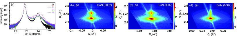
The HRXRD and RSM measurements have been carried out with a PANalytical’s X’Pert PRO Materials Research Diffractometer (MRD) equipped with a hybrid monochromator with a 1/4∘ divergence slit. The diffracted beam is measured with a solid-state PixCel detector used as 256-channels detector with a 11.2 mm anti-scatter slit. In the radial scans for values between and (not shown here) only reflections from the -Al2O3 substrate, from the GaN buffer/reservoir and from g-AlxGa1-xN (AlxGa1-xN:Si) are detectable. The radial HRXRD spectra of the symmetric (0004) reflection for the whole series of samples investigated in the present study are shown in Fig. 1(a). While a sharp peak related to the AlxGa1-xN (0004) reflection is detected for sample S0, for samples S1-S5 containing a g-AlxGa1-xN the multiple peaks at the AlxGa1-xN (0004) reflection are fingerprints of the gradient in the Al concentration.
In order to gain a deeper insight into the distribution of Al in the samples, RSM of the symmetric (0002) reflections have been acquired and are reported in Figs. 1 (b)-(d) for samples S0, S1, and S4. The broadening in the direction Qx ( - scan) is determined by the tilt and finite lateral coherence length of mosaic blocks Moram and Vickers (2009). In Figs. 1 (c)-(d), the elongation along the Qz direction points to a pseudomorphically grown AlxGa1-xN layer with graded Al concentration on GaN. However, for sample S0 –as evidenced in Fig. 1 (b)– this elongation of AlxGa1-xN (0002) along Qz is not detected, confirming the presence of a non-graded AlxGa1-xN:Si layer with a constant 25%.
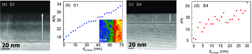
Measurements of TEM also in STEM mode are performed in a FEI Titan Cube 80-300 operating at 300 keV and in a JEOL 2010F working at 200 KeV. Bright/dark-field BF/DF, HRTEM and HAADF are employed to analyse the structure of the sample, while chemical mapping is achieved through EELS analysis. Cross-section TEM specimens are prepared by mechanical polishing, dimpling and final ion milling in a Gatan Precision Ion Polishing System. The TEM micrograph of sample S1 reported in Fig. 2 (a) evidences the Al composition changes in the 75 nm thick g-AlxGa1-xN (: 0%37%) layer, and the EELS data in Fig. 2 (b) confirm the increase of the Al concentration in the g-AlxGa1-xN corresponding to the nominal increment of Al flow rate during the process. On the other hand, for the 30 nm thin g-AlxGa1-xN (: 0%37%) layer in S4, from the TEM image in Fig. 2 (c) it is not possible to appreciate the contrast between the g-AlxGa1-xN regions with different Al content, but the monotonic increment of the Al concentration with the thickness is confirmed by the EELS data in Fig. 2 (d). This is in accord with the presence of a 5 nm wide intermixing region around the interfaces between nominal variations in Al detected HAADF measurements as reported in the inset to Fig. 2 (b) for the interface AlxGa1-xN/GaN.
For the Hall effect measurements and magnetoresistance studies, a four-probe van der Pauw geometry is employed. The Hall effect measurements are carried out in dc mode, while the MR studies are performed using a low frequency ac technique. The ohmic contacts for all samples consist of a Ti/Au/Al/Ti/Au metal stack deposited in an e-beam evaporation chamber and then annealed at 750∘C in N2 atmosphere for 30 seconds.
III Results and discussion
The above results of structural and chemical analysis of the samples confirm the presence of a controlled concentration gradient of Al in the wanted volume and the consequent non-vanishing divergence of the polarization is expected to determine the electrical properties of the samples.
The combination of spontaneous and piezoelectric polarization P(x) for an AlxGa1-xN layer coherently strained to GaN is given by Ambacher et al. (2002):
| (1) |
for a fixed concentration of Al. However, in the presence of a gradient in the content of Al over the AlxGa1-xN layer thickness, the spatial change of the polarization leads to doping driven by dipole engineering and the induced charge NDp is given by Wood and Jena (2008):
| (2) |
where x0 is the concentration of Al at a position from the interface with the buffer and along the growth direction ().
By applying Eq. 2 and by implementing the Al concentration as obtained from EELS measurements, the value of NDp calculated at 30 nm from the interface with the buffer for sample S4, is estimated to be (1.251019) cm-3. A remarkable feature of this method of doping is that the doping level can be controlled by tuning the alloy composition and/or the thickness of the graded layer. The de Broglie wavelength is 17 nm for non-degenerate carrier densities, while the Fermi-wavelength for degenerate systems (1020 cm-3) is calculated to be 30 nm. Any thickness of the graded layer which is smaller than these two characteristic lengths, leads to the formation of a quasi-2DEG. However, for wide slabs of graded regions with , the electron gas is 3D.
In Fig. 3 (a) the electron concentration and in Fig. 3 (b) the Hall mobilities as a function of temperature in the range 40 KT300 K are reported for samples S0-S4 (S5 is semi-insulating). According to the curves in Fig. 3 (a), all the g-AlxGa1-xN samples have carrier densities cm-3, i.e. well above the critical concentration for the metal-to-insulator transition (MIT) in n-GaN:Si Stefanowicz et al. (2014). By exploiting the Mott model, where the critical carrier concentration is related to the Bohr radius of the relevant dopant aB as Dietl (2008), we calculate for n-AlN, n-Al0.30Ga0.70N and n-Al0.40Ga0.60N as (21018) cm-3, (2.71018) cm-3 and (41018) cm-3, respectively. By comparing these values with the Hall data, we conclude that the reference Al0.25Ga0.75N:Si is doped degenerately and is above the MIT. The polarization doped g-AlxGa1-xN samples also exhibit carrier concentrations far above the Mott limit for the corresponding AlxGa1-xN systems doped with donor impurities like Si. These results indicate that polarization induced doping in the studied graded AlxGa1-xN drives such systems to a degenerate regime with the formation of a 3DES.
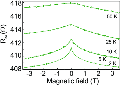
Since all the samples discussed here have far above the Mott MIT limit, the graded Al1-xGaxN layers are expected to be in a weak localization regime Stefanowicz et al. (2014). This is confirmed by the observation of negative MR (positive magnetoconductance) in the magnetoresistance data acquired as a function of the applied magnetic field and for various temperatures 2 KT50 K, as reported in Fig. 4 for sample S4. If the 3DES is spread over a thickness , then the sheet carrier density of the 3DES is calculated to be . For S4, this thickness is then 30 nm, pointing to a 5 nm depletion of the 3DES from the surface potential.
The Hall parameters at 50 K and 300 K for samples S0-S5 are listed in Table I.
| Sample | Structure | (reservoir)* | (50 K) | (300 K) | (50 K) | (300 K) | (10-2) | |
|---|---|---|---|---|---|---|---|---|
| (nm) | (cm-3) | ( cm-3) | ( cm-3) | (cmVs) | (cmVs) | (cm) | ||
| S0 | AlxGa1-xN:Si/ | 1016 | 2.66 | 5.11 | 15.88 | 13 | 9.68 | |
| /u-GaN | ||||||||
| (100/1000) | ||||||||
| S1 | g-AlxGa1-xN/ | 1016 | 3.16 | 3.86 | 15 | 15.57 | 11.03 | |
| /u-GaN | ||||||||
| (75/1000) | ||||||||
| S2 | g-AlxGa1-xN/ | 1016 | 1.27 | 2.74 | 44.5 | 97.74 | 2.3 | |
| /u-GaN | ||||||||
| (35/1000) | ||||||||
| S3 | g-AlxGa1-xN/ | 1019 | 60.2 | 61.5 | 117 | 158.34 | 0.0635 | |
| /GaN:Si/ | ||||||||
| /SI-GaN:Mn | ||||||||
| (75/500/1000) | ||||||||
| S4 | g-AlxGa1-xN/ | 1019 | 137 | 128 | 155 | 215 | 0.027 | |
| /GaN:Si/ | ||||||||
| /SI-GaN:Mn | ||||||||
| (35/500/1000) | ||||||||
| S5 | g-AlxGa1-xN/ | SI | SI | SI | SI | SI | SI | |
| /SI-GaN:Mn | ||||||||
| (75/1000) |
*Reservoir/buffer: layer on which g-AlxGa1-xN and/or AlxGa1-xN:Si are grown.
Sample S0 shows a carrier density of (21018) cm-3 at 300 K, which decreases with temperature. This sample is at the boundary of the MIT transition and for T40 K it can be driven to a non-degenerate electronic state. For samples S1 and S2, where the g-AlxGa1-xN layer is grown on an u-GaN buffer with 1016cm-3, the bulk carrier density at 300 K is (31018) cm-3, and it remains substantially constant over the measured temperature range. However, for samples S3 and S4, grown on a degenerate GaN:Si reservoir with =(1.21019) cm-3, one can observe an enhanced carrier density, reaching (61019) cm-3 for S3 and (1.41020) cm-3 for S4. These values are greater than those observed for n-GaN:Si [Stefanowicz et al., 2014] and for 3DES in MBE g-AlxGa1-xN/GaN systems Jena et al. (2003); Li et al. (2012). The difference between S3 and S4 resides solely in the thickness of the g-AlxGa1-xN layer. It is observed that sample S4 with a 35 nm thickness of the graded layer shows higher carrier concentration when compared to S3, where the thickness of g-AlxGa1-xN is 75 nm. Also, from the observed carrier densities of the graded layers it can be concluded that the bulk concentration of carriers in the GaN reservior/buffer plays a dominant role in determining the amount of charge carriers induced in a polarization doped g-AlxGa1-xN system, where the graded layer grown on a degenerate GaN:Si shows a carrier concentration up to two orders of magnitude higher than when the g-AlxGa1-xN layer is deposited on an u-GaN buffer. Furthermore, the absence of significant free charge carriers in the buffer, like in S5, keeps g-AlxGa1-xN semi-insulating.
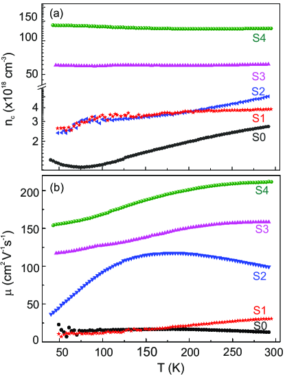
From Fig. 3 (b) we observe for samples S1-S4 carrier mobilities which are comparable Li et al. (2012) or slightly lower than those observed in 3DES fabricated by MBE Jena et al. (2002, 2003). However,the Al concentration in the above mentioned works had a gradient in the range : 0%20%, while all the samples considered in this work have a Al gradient : 0%37%. A maximum mobility of 210 cm2/Vs is achieved in S4, while for S1 a value of 15.57 cm2/Vs at 300 K is obtained. The samples S3 and S4 –with a rich reservoir of electrons in the GaN:Si buffer– have higher mobilities compared to S1 and S2 deposited on u-GaN. From here it can be inferred, that the electronic properties (carrier concentration) of the reservoir/buffer directly affect the mobility in the 3DES. The dislocation density and the dislocation-related scattering of the charge carriers in the 3DES play also a role in determining the carrier mobility of the 3DES. From weak beam dark field image TEM data on sample S1, the screw- and edge-dislocation densities are estimated in (1.0108) cm-2 and (8.1109) cm-2, respectively, while for sample S4, are of the order of (6.62108) cm-2 and (1.261010) cm-2. In the calculation, the average specimen thickness is established by counting the dark fringes in the BF image under two beam conditions, and the extinction distance of GaN used in the calculation is 56 nm [Kong et al., 2002].
Dislocations affect the carrier transport mostly through two mechanisms, namely the local deformation they induce in the lattice and the accumulation of static charges along the dislocation line or the core effect scattering. According to theoretical models, the main contribution to electron scattering due to dislocations in wz-III-nitride systems, originates from -edge dislocations and from the edge component of () mixed dislocations. The contribution from -screw dislocations was shown to have a negligible effect on the electron scattering (and consequently on the electron mobilities) in AlxGa1-xN/GaN based structures Carosella and Farvacque (2008). From TEM measurements it is seen that the edge dislocation density in sample S4 is 1.55 times greater than in S1, but magnetotransport measurements reveal a Hall mobility of 210 cm2/Vs in S4, much greater than the 15 cm2/Vs of S1. This behaviour can be explained considering the carrier densities of the two samples. While in S4 we observe a carrier density of (1.31020) cm-3, the one measured in S1 is (3.8) cm-3. With an increase in carrier density, the dislocation band located below the conduction band becomes narrower, reducing the strength of the scattering potential. Thus, despite a higher edge dislocation density, we observe a greater electron mobility in sample S4 compared to S1. Alloy disorder scattering and interface scattering additionaly affect the observed mobility in the 3DES samples.
IV Conclusions
In summary, g-AlxGa1-xN layers on buffer/reservoir GaN layers with different electron concentrations have been grown by MOVPE and thoroughly analysed. The compositional grading of the AlxGa1-xN layer leads to the formation of a 3DES, whose Hall concentration depends on the electron concentration in the buffer/reservoir. The conductivity of the samples increases with increasing and this can be achieved either by augmenting the gradient range of the Al content while not varying the thickness of the graded layer, or by decreasing the layer thickness for a fixed range of the gradient, or by using a buffer/reservoir with a carrier concentration orders of magnitude higher than the one of u-GaN. The observed magnetoresistance points to quantum corrections to the conductivity, due to weak localization Stefanowicz et al. (2014). With the present work it is shown that controllable g-AlxGa1-xN leading to a 3DES can be fabricated in a MOVPE process. The realization of such degenerate AlxGa1-xN-based systems opens wide perspectives for the fabrication of efficient electrodes in nitride-based deep UV LEDs and lasers, active layers for diodes, transistors and spin devices like nitride-based spin field effect transistors.
Acknowledgements
This work was supported by the Austrian Science Foundation – FWF (P22477 and P24471 and P26830), by the NATO Science for Peace Programme (Project No. 984735) and by the EU Framework Programmes: CAPACITIES project REGPOT-CT-2013-316014 (EAgLE), and FunDMS Advanced Grant of the European Research Council (ERC grant No. 227690).
References
- Nakamura et al. (1993) S. Nakamura, M. Senoh, and T. Mukai, Appl. Phys. Lett. 62, 2390 (1993).
- Nakamura (1995) S. Nakamura, J. Vac. Sci. Technol. A 13, 705 (1995).
- Gutt et al. (2012) R. Gutt, T. Passow, M. Kunzer, W. Pletschen, L. Kirste, K. Forghani, F. Scholz, K. Köhler, and J. Wagner, Applied Physics Express 5, 032101 (2012).
- Morkoç (2008) H. Morkoç, Handbook of Nitride Semiconductors and Devices, Vol. 2 (Wiley-VCH Verlag GmbH & Co. KGaA, 2008).
- Yoshida et al. (2008) H. Yoshida, Y. Yamashita, M. Kuwabata, and H. Kan, Nat. Photonics 2, - (2008).
- Shur (1998) M. Shur, Solid. State. Electron. 42, 2131 (1998).
- Yeluri et al. (2015) R. Yeluri, J. Lu, C. A. Hurni, D. A. Browne, S. Chowdhury, S. Keller, J. S. Speck, and U. K. Mishra, Appl. Phys. Lett. 106, - (2015).
- Mishra (2002) U. K. Mishra, Proc. IEEE 90, 1022 (2002).
- Sun et al. (2015) H. Sun, M. M. Bajo, M. J. Uren, and M. Kuball, Appl. Phys. Lett. 106, 043505 (2015).
- Bernardini et al. (1997a) F. Bernardini, V. Fiorentini, and D. Vanderbilt, Phys. Rev. B 56, R10024 (1997a).
- Bernardini et al. (1997b) F. Bernardini, V. Fiorentini, and D. Vanderbilt, Phys. Rev. Lett. 79, 3958 (1997b).
- Ambacher et al. (2002) O. Ambacher, J. Majewski, C. Miskys, A. Link, M. Hermann, M. Eickhoff, M. Stutzmann, F. Bernardini, V. Fiorentini, V. Tilak, B. Schaff, and L. F. Eastman, J.Phys.:Condens.Mater 14, 3399 (2002).
- Bernardini and Fiorentini (2001) F. Bernardini and V. Fiorentini, Phys. Rev. B 64, 085207 (2001).
- Smorchkova et al. (1999) I. P. Smorchkova, C. R. Elsass, J. P. Ibbetson, R. Vetury, B. Heying, P. Fini, E. Haus, S. P. DenBaars, J. S. Speck, and U. K. Mishra, J. Appl. Phys. 86, 4520 (1999).
- Schmult et al. (2006) S. Schmult, M. J. Manfra, A. Punnoose, A. M. Sergent, K. W. Baldwin, and R. J. Molnar, Phys. Rev. B 74, 033302 (2006).
- Hsu and Walukiewicz (2001) L. Hsu and W. Walukiewicz, J. Appl. Phys. 89, 1783 (2001).
- Palacios et al. (2005) T. Palacios, A. Chakraborty, S. Rajan, C. Poblenz, S. Keller, S. DenBaars, J. Speck, and U. Mishra, Electron Device Letters, IEEE 26, 781 (2005).
- Jena et al. (2002) D. Jena, S. Heikman, D. Green, D. Buttari, R. Coffie, H. Xing, S. Keller, S. DenBaars, J. S. Speck, U. K. Mishra, and I. Smorchkova, Appl. Phys. Lett. 81, 4395 (2002).
- Jena et al. (2003) D. Jena, S. Heikman, J. Speck, A. Gossard, U. Mishra, A. Link, and O. Ambacher, Phys. Rev. B 67, 153306 (2003).
- Li et al. (2013) S. Li, T. Zhang, J. Wu, Y. Yang, Z. Wang, Z. Wu, Z. Chen, and Y. Jiang, Appl. Phys. Lett. 102, 062108 (2013).
- Simon et al. (2010) J. Simon, V. Protasenko, C. Lian, H. Xing, and D. Jena, Science 327, 60 (2010).
- Walukiewicz (2001) W. Walukiewicz, Physica B: Condensed Matter 302–303, 123 (2001).
- Borisov et al. (2005) B. Borisov, V. Kuryatkov, Y. Kudryavtsev, R. Asomoza, S. Nikishin, D. Y. Song, M. Holtz, and H. Temkin, Appl. Phys. Lett. 87, 132106 (2005).
- Taniyasu et al. (2006) Y. Taniyasu, M. Kasu, and T. Makimoto, Nature 441, 325 (2006).
- Golam Sarwar et al. (2015) A. T. M. Golam Sarwar, S. D. Carnevale, T. F. Kent, F. Yang, D. W. McComb, and R. C. Myers, Appl. Phys. Lett. 106, 032102 (2015).
- Li et al. (2015) C. Li, Z. Li, D. Peng, J. Ni, L. Pan, D. Zhang, X. Dong, and Y. Kong, Semicond. Sci. Technol. 30, 035007 (2015).
- Kivisaari et al. (2013) P. Kivisaari, J. Oksanen, and J. Tulkki, Appl. Phys. Lett. 103, 211118 (2013).
- Park et al. (2015) P. S. Park, S. Krishnamoorthy, S. Bajaj, D. Nath, and S. Rajan, IEEE Elect. Dev. Lett. 36, 226 (2015).
- Murzin et al. (1998) S. S. Murzin, A. G. M. Jansen, and P. v. d. Linden, Phys. Rev. Lett. 80, 2681 (1998).
- Halperin (1987) B. I. Halperin, Jpn. J. App. Phys. 26, 1913 (1987).
- Kohmoto et al. (1992) M. Kohmoto, B. I. Halperin, and Y.-S. Wu, Phys. Rev. B 45, 13488 (1992).
- Koshino et al. (2001) M. Koshino, H. Aoki, K. Kuroki, S. Kagoshima, and T. Osada, Phys. Rev. Lett. 86, 1062 (2001).
- Koshino and Aoki (2003) M. Koshino and H. Aoki, Phys. Rev. B 67, 195336 (2003).
- Brey and Halperin (1989) L. Brey and B. I. Halperin, Phys. Rev. B 40, 11634 (1989).
- Simon et al. (2006) J. Simon, A. K. Wang, H. Xing, S. Rajan, and D. Jena, Appl. Phys. Lett. 88, 042109 (2006).
- Li et al. (2012) S. Li, M. E. Ware, J. Wu, V. P. Kunets, M. Hawkridge, P. Minor, Z. Wang, Z. Wu, Y. Jiang, and G. J. Salamo, J. Appl. Phys. 112, 053711 (2012).
- Moram and Vickers (2009) M. A. Moram and M. E. Vickers, Reports on Progress in Physics 72, 036502 (2009).
- Wood and Jena (2008) C. Wood and D. Jena, eds., Polarization Effects in Semiconductors: From Ab Initio Theory to Device Applications (Springer US, 2008).
- Stefanowicz et al. (2014) W. Stefanowicz, R. Adhikari, T. Andrearczyk, B. Faina, M. Sawicki, J. A. Majewski, T. Dietl, and A. Bonanni, Phys. Rev. B 89, 205201 (2014).
- Dietl (2008) T. Dietl, J. Phys. Soc. Jpn. 77, 031005 (2008).
- Kong et al. (2002) X. Kong, G. Q. Hu, X. F. Duan, Y. Lu, and X. L. Liu, Appl. Phys. Lett. 81, 1990 (2002).
- Carosella and Farvacque (2008) F. Carosella and J.-L. Farvacque, J.Phys:Condens. Mater 20, 325210 (2008).