Helicity sensitive terahertz radiation detection by
dual-grating-gate high electron mobility transistors
Abstract
We report on the observation of a radiation helicity sensitive photocurrent excited by terahertz (THz) radiation in dual-grating-gate (DGG) InAlAs/InGaAs/InAlAs/InP high electron mobility transistors (HEMT). For a circular polarization the current measured between source and drain contacts changes its sign with the inversion of the radiation helicity. For elliptically polarized radiation the total current is described by superposition of the Stokes parameters with different weights. Moreover, by variation of gate voltages applied to individual gratings the photocurrent can be defined either by the Stokes parameter defining the radiation helicity or those for linear polarization. We show that artificial non-centrosymmetric microperiodic structures with a two-dimensional electron system excited by THz radiation exhibit a photocurrent caused by the combined action of a spatially periodic in-plane potential and spatially modulated light. The results provide a proof of principle for the application of DGG HEMT for all-electric detection of the radiation’s polarization state.
pacs:
78.67.De,07.57.Kp,85.30.Tv,85.35.-pI I. Introduction
Field-effect-transistors (FETs) have emerged as promising devices for sensitive and fast room temperature detection of terahertz (THz) radiation knaprev2013 ; knaptredicuccirev2013 . They are considered as a good candidate for real-time THz imaging and spectroscopic analysis Boppel2012 ; Muravev2012 as well as future THz wireless communications Tonouchi2007 . Devices employing plasmonic effects in FETs have already been applied for room temperature detection of radiation with frequencies from tens of GHz up to several THz and enable the combination of individual detectors in a matrix. They are characterized by high responsivity (up to a few kV/W), low noise equivalent power (down to 10 pW/), fast response time (tens of picoseconds) and large dynamic range (linear power response up to 10 kW/cm2), see e.g. Ref.knaptredicuccirev2013 ; 9 ; 14Roj ; 11 ; Watanabe ; But2014 ; Knap2014 . The operation principle of FET THz detectors used so far is based on the nonlinear properties of the two-dimensional (2D) plasma in the transistor channel. The standard Dyakonov-Shur model Dyakonov assumes that radiation is coupled to the transistor by an effective antenna, which generates an voltage predominantly on one side of the transistor. Both resonant 98 and non-resonant 99 regimes of THz detection have been studied. While research aimed to development of THz FET detectors is focused on single gate structures recently several groups have shown that higher sensitivities are expected for structures with periodic symmetric and asymmetric metal stripes or gates Watanabe ; 19w ; 116 ; 20w ; 16w ; 18w ; 31 ; 115 ; 35 ; 31Roj . In particular, dual-grating-gate FET are considered as a good candidate for sensitive THz detection. The first data obtained on dual-gated-structures demonstrated a substantial enhancement of the photoelectric response and an ability to control detector parameters by variation of individual gate bias voltage Watanabe . At the same time, THz electric field applied to FETs with asymmetric periodic dual gate structure is expected to give rise to electronic ratchet effects 28 ; 30 ; 29 ; 31Roj ; 33Roj (for review see 30 ) and plasmonic ratchet effects 36 . Besides improving the figure of merits of FET detectors, ratchet effects may also result in new functionalities. In particularly, they may induce photocurrents driven solely by the radiation helicity.
Here, we report on the observation of a radiation helicity sensitive photocurrent excited by THz radiation in dual-grating-gate InAlAs/InGaAs/InAlAs/InP high electron mobility transistors (HEMT). We show that artificial non-centrosymmetric microperiodic structures with a two-dimensional electron system excited by THz radiation exhibit a photocurrent caused by the lateral asymmetry of the applied static potential and terahertz electric field. We demonstrate that depending on gate voltages applied to the individual gratings of the dual-grating-gate the response can be proportional to either the Stokes parameters Saleh defining the radiation helicity or those for linear polarization. As an important result, for a wide range of gate voltages we observed a photocurrent being proportional to the radiation helicity , where and are intensities of right- and left-handed circularly polarized light. For the circular photocurrent measured between source and drain contacts changes its sign with the inversion of the radiation helicity. This observation is of particular importance for a basic understanding of plasmon-photogalvanic and quantum ratchet effects. It also has a large potential for the development of an all-electric detector of the radiation’s polarization state, which was so far realized applying less sensitive photogalvanic effects only 122 ; 123 ; 124 . The observed phenomena is discussed in the framework of electronic ratchet 35 ; 30 ; 29 ; 33Roj ; 31Roj and plasmonic ratchet effects excited in a 2D electron system with a spatially periodic dc in-plane potential Watanabe ; 35 ; 36 .
II II. Experimental Technique
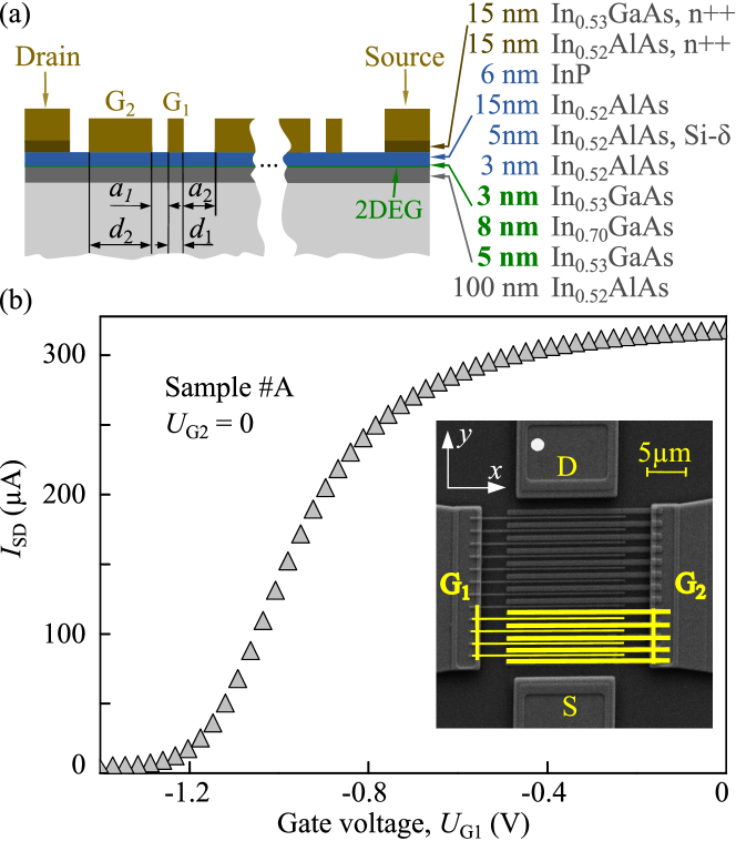
The device structure is based on an InAlAs/InGaAs/InAlAs/InP high-electron mobility transistor (HEMT) and incorporates doubly inter-digitated grating gates (DGG) G1 and G2. A sketch and a photograph of the gates are shown in Fig. 1(a) and inset in Fig. 1(b). The 2D electron channel is formed in a quantum well (QW) at the heterointerface between a 16 nm-thick undoped InGaAs composite channel layer and a 23 nm-thick, Si-doped InGaAs carrier-supplying layer. The electron density of the 2DEG is about cm2, electron effective mass normalized on free-electron mass and room temperature mobility are and = 11000 cm2/(Vs), respectively. The DGG gate is formed with 65 nm-thick Ti/Au/Ti by a standard lift-off process. The footprint of the narrower gate fingers G1 was defined by an E-beam lithography, whereas that of the wider gate fingers G2 was defined by a photolithography. In all studied structures, the metal fingers of the grating gates G1 and G2 have the same length, being = 200 nm and = 800 nm. The spacing between narrow and wide DGG fingers is asymmetric with = 200 nm and = 400 nm, see Fig. 1. The size of the active area, covered with the grating is about 20 m20 m. Ohmic contacts, forming source and drain of HEMTs, were fabricated by highly doped 15 nm thick InAlAs and InGaAs layers. The axis along the gate’s fingers is denoted as and that along source and drain as . The characteristic source/drain current - gate voltage dependence obtained by transport measurement is shown for sample #A in Fig. 1(b).
All experiments are performed at room temperature. The HEMT structures were illuminated with polarized THz and microwave (MW) radiation at normal incidence. For optical excitation we used low power optically pumped CH3OH THz laser 3aa ; karch2010 and Gunn diodes providing monochromatic radiation with frequencies = 2.54 THz and 95.5 GHz, respectively. The radiation peak power , being of the order of several milliwats at the sample’s position, has been controlled by pyroelectric detectors and focused onto samples by parabolic mirrors (THz laser) or horn antenna (Gunn diode). The spatial beam distribution of THz radiation had an almost Gaussian profile, checked with a pyroelectric camera edge ; Glazov2014 . THz laser radiation peak intensity, , for laser spot being of about 1.2 mm diameter on the sample, was W/cm2. The profile of the microwave radiation and, in particular, the efficiency of the radiation coupling to the sample couldn’t be determined with satisfactory accuracy. Thus, all microwave data are given in arbitrary units. The polarization state of THz radiation has been varied applying crystal quartz /4- or /2-plates book . To obtain circular and elliptically polarized light the quarter-wave plate was rotated by the angle, , between the initial polarization plane and the optical axis of the plate. The radiation polarization states for several angles are illustrated on top of Fig. 2. Orientation of the linearly polarized radiation is defined by the azimuth angle , with chosen in such a way that the electric field of incident linearly polarized light is directed along -direction. Different orientation of linearly polarized MW radiation were obtained by rotation of a metal wire grid polarizer. The photocurrent excited between source and drain is measured across a 50 load resistor applying the standard lock-in technique.
III III. Photocurrent experiment
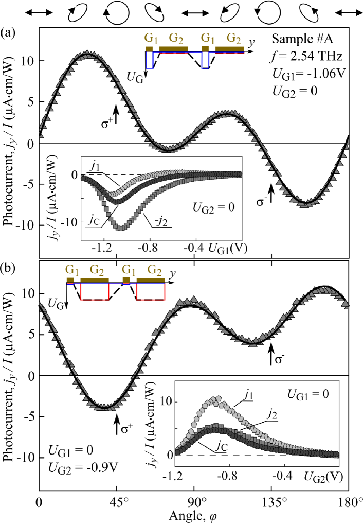
Illuminating the structure with elliptically (circular) polarized radiation of terahertz laser operating at frequency = 2.54 THz we observed a current strongly depending on the radiation polarization. Figure 2(a) shows the photocurrent as a function of the phase angle defining the radiation polarization state. The data are obtained for zero gate voltage at the gate 2, = 0 and = -1.06 V. The principal observation is that for right- () and left-handed () polarizations, i.e., for and , the signs of the photocurrent are opposite. The overall dependence is well described by
| (1) |
and corresponds to the superposition of the Stokes parameters with different weights given by the coefficients , , , and , which in the experimental geometry applying rotation of quarter-wave plate the Stokes parameters change after
| (2) | |||
| (3) | |||
| (4) | |||
| (5) |
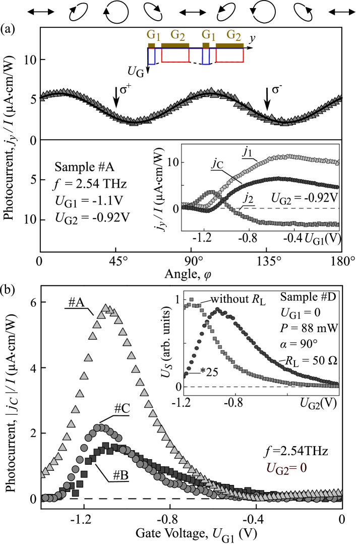
Here determines the radiation intensity, and define the linear polarization of radiation in the and rotated by coordinate frames, and describes the degree of circular polarization or helicity of radiation. Consequently individual photocurrent contributions in Eq. (1) are induced by unpolarized, linearly or circularly polarized light components. While the polarization dependence given by Eq. (1) has been detected for arbitrary relations between voltages applied to the first and second gates, the magnitude and even the sign of the individual contributions can be controlled by the gate voltages. The inset in Fig. 2(a) shows a gate dependence of the polarization dependent contributions to the total photocurrent footnote . The dependence on the gate voltage is obtained for zero biased second gate. Photocurrent measured in the close circuit configuration with shows a maximum amplitude for V. For open circuit configuration the measured photovoltage increases at larger negative bias voltages and achieves maximum at the threshold voltage, V. Corresponding data will be presented and discussed below. While the non-monotonic behavior of the signal for gate voltage variation is well known for FET detectors knaprev2013 ; knaptredicuccirev2013 ; 30w the signal sign inversion upon a change of the radiation polarization, see Fig. 2(a), is generally not expected for standard Dyakonov-Shur FET detectors indicating crucial role of the lateral superlattice in the photocurrent generation. To demonstrate that the observed effect indeed stems from the lateral asymmetry of the periodic potential we interchanged the voltages applied to the gates. Figure 2(b) shows the results obtained for zero gate voltage at the first gate and V at the second one. The figure reveals that changing the sign of the lateral potential asymmetry, see insets of Fig. 2(a) and (b), results in the sign inversion of all contributions besides the polarization independent offset. The situation holds for almost all values of , see the insets in Fig. 2(a) and (b). Significantly, the proper choice of the relation between amplitudes of the individual gate potentials allows one to suppress completely one or the other photocurrent contribution. Figure 3(a) demonstrates that for close values of gate voltages the circular photocurrent vanishes (corresponding potential profile for = -1.1 V and = -0.9 V is shown in the inset in Fig. 3). The interplay of the contributions upon variation of and for fixed = -1.1 V is shown in the inset in Fig. 3(a). It is seen that for nonzero second gate voltage the circular, , and linear, , photocurrent contributions change their direction with increasing . Moreover, the inversions take place at different voltages. This fact can be used to switch on and off the circular photocurrent contribution.
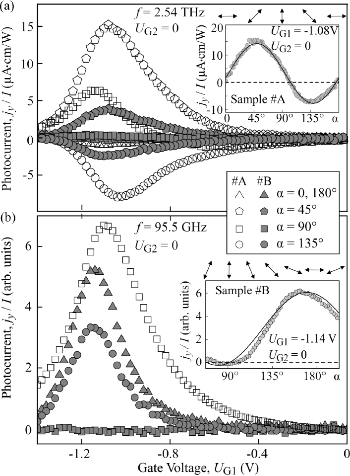
To support the conclusion that and photocurrent contribution are caused by the linear polarized light component we carried out additional measurements applying linearly polarized light. The gate dependence of the normalized photocurrent measured for samples #A and #B for several azimuth angles are shown in Fig. 4(a). The inset in this figure presents the dependence of on the electric field orientation. The polarization dependence is well described by the Eq. (1) taking into account that for linearly polarized light the last term vanishes and the Stokes parameters are given by
Here defines the orientation of the polarization plane and is the angle between the initial polarization plane and the optical axis of the half-wave plate. The magnitudes and signs of the coefficients , , and used for the fit coincide with that applied for fitting of -dependencies obtained at the same gate voltages. These results demonstrate that photocurrents and measured in set-up applying quarter-wave plate are indeed controlled by the degree of linear polarization of elliptically polarized radiation.
The polarization sensitive photocurrent has been observed in all studied devices of similar design and arbitrary relation between second and first gate potentials. The photocurrent can always be well described by Eq. (1). Figure 3(b) summarizes the data on the helicity driven photocurrent detected in three HEMT structures upon change of and for . In all samples we detected similar dependencies of the photocurrent characterized by close maximum positions but different signal magnitudes. The data of Fig. 3(b) as well as circles in its inset are obtained in the close circuit configuration applying 50 load resistance. The non-monotonic behavior of the photosignal measured in this geometry is caused by the interplay of the potential asymmetry, increasing with raising second gate voltage, and raising of the sample resistance for large gate voltages. For the open circuit geometry (signal is fed to the high input impedance of lock-in amplifier) the maximum of the signal is detected for gate voltages being equal to the threshold voltage, , see squares in the inset in Fig. 3(b). Following Ref. Watanabe we estimate from the voltages measured in open circuit geometry the voltage responsivities for the signals corresponding to the photocurrents and as V/W and 0.15 V/W, respectively. Here the total power of the source at the detector plane, radiation beam spot area, and m2 transistor area. The voltage responsivities, being rather low as compared to that typically obtained for plasmonic FET detectors, indicates the necessity of further optimization of the structure design. Finally, we note that measurements applying microwave radiation show that for lower frequencies the polarization behavior changes qualitatively. Instead of the sign-alternating dependencies discussed above the signal now varies after , see inset in Fig. 4(b). This observation is in a good agreement with the Dyakonov-Shur theory Dyakonov and was reported for many conventional plasmonic FET detectors, see e.g. knaprev2013 ; knaptredicuccirev2013 . The gate voltage dependence of the response shown in Fig. 4 also reproduces well the results previously obtained for similar structures Watanabe ; Coquillat2014 . Even the fact that the maximum of the signal in various structures has been obtained for different directions of the electric field vector in respect to -direction (source-drain) has already been reported for these transistors and attributed to the antenna coupling of MW radiation to transistor, see Ref. Coquillat2014 .
IV IV. Discussion
The observation of the circular photocurrent and the sign-alternating linear photocurrent reveals that a microscopic process actuating these photocurrents goes beyond the plasmonic Dyakonov-Shur model typically applied to discuss operation of FETs THz detectors. Indeed, as addressed above, the latter implies an oscillating electric field along source-drain direction (-direction) yielding sign conserving variation upon rotation of polarization plane, footnote2 . As recently shown in Ref. 117 ; 118 , the Dyakonov-Shur model in fact may result in the circular photocurrent but only due to interference effects of two different channels and two interacting antennas in small size special design FETs - the model which can hardly be applied to the large DGG samples used in our experiments. At the same time, the observed polarization behavior is characteristic for the electronic ratchet effects excited in asymmetric periodic structures 28 ; 30 ; 29 ; 33Roj and linear/circular plasmonic ratchet effects 35 ; 36 . The ratchet currents arise due to the phase shift between the periodic potential and the periodic light electric field resulting from near field diffraction in a system with broken symmetry. Microscopic theory developed in Ref. 29 shows that the helicity dependent photocurrent appear because the carriers in the laterally modulated quantum wells move in two directions and are subjected to the action of the two-component electric field. Symmetry analysis of the photocurrent shows that in our DDG structures described by C1 point group symmetry footnote3 it varies with radiation polarization after Eq. (1), being in agreement with experimental observation shown in Figs. 2, 3 and 4(a). Moreover, as the ratchet photocurrents are proportional to the degree of the in-plane asymmetry, they reverse the sign upon inversion of static potential asymmetry. Exactly this behavior has been observed in experiment, see Fig. 2 (a) and (b). The proportionality to the degree of lateral asymmetry also explain the increase of the signal with raising voltage applied to one gate at constant voltage by the other. The interplay of the degree of lateral asymmetry and periodic modulation of THz electric field results in the complex gate-voltage dependence, in particular, for . As the different individual contributions to the total current effect might imply different microscopic mechanisms of the photocurrent formation, their behavior upon change of external parameters can distinct from each other. This would result in a sign-alternating gate-voltage behavior, in particular for the range of comparable and , like it is observed in experiment, see Fig. 2 (c). While all qualitative features of the observed phenomena can be rather good described in terms of ratchet effects we would like to address another possible effect, which might trigger the helicity-driven photocurrent. It could be the differential plasmonic drag effect in the two-dimensional structure with an asymmetric double-grating gate considered in Refs. 35 ; Popov2015 . As shown in Ref. 35 for a periodic AlAs/InGaAs/InAlAs/InP structure and linearly polarized THz radiation, photon drag effect can be comparable in strength with the plasmonic ratchet effect at THz frequencies. As the circular photon drag effect has been observed in different low dimensional materials karch2010 ; Shalygin2006 we can expect that modification of the theory developed in 35 can also yield helicity driven plasmonic drag current compatible with the ratchet one.
Finally, we note that the ratchet effects (either electronic or plasmonic) can be greatly increased due to the resonant enhancement of the near-field in two-dimensional electron system at the plasmon resonance excitation as it was shown for the plasmonic ratchet in Refs. 31Roj ; 36 . The resonant plasmon condition , see Ref. Dyakonov can be well satisfied in our structure ( at 2.54 THz). As shown in Ref. 31Roj , the fundamental plasmon resonance is excited in a similar structure at frequency around 2 THz. Therefore, the plasmon resonance excitation can contribute to the observed ratchet effects independently of particular microscopic mechanisms of the ratchet photocurrent formation. The measurements in a broader THz frequency range could elucidate the role of the plasmonic resonance excitation in the ratchet photocurrent enhancement.
V V. Summary
To summarize, our measurements demonstrate that dual-grating-gate InAlAs/InGaAs/InAlAs/InP excited by terahertz radiation can yield a helicity sensitive photocurrent response at THz frequencies. We show, that HEMTs with asymmetric lateral superlattice of gate fingers with unequal widths and spacing can be applied for generation of a photocurrent defined by linearly and circularly radiation polarization components. Moreover, one can obtain photoresponse being proportional to one of the Stokes parameters simply by variation of voltages applied to the individual gates. The photocurrent formations can be well described in terms of ratchet effects excited by terahertz radiation. By that the lateral grating induces a periodical lateral potential acting on the 2D electron gas in QW. This grating also modulates the incident radiation in the near field and hence in the plane of the 2DES, resulting in circular, linear and polarization-independent ratchet effects. While the responsivity of the polarization dependent response is lower than that reported for FET transistors it can be substantially improved by optimization of the structure design leading the resonant enhancement of the ratchet effects the plasmon resonance excitation.
Acknowledgements.
We thank V. Popov for helpful discussions. The financial support from the DFG (SFB 689) is gratefully acknowledged.References
- (1) W. Knap and M. Dyakonov, Plasma wave THz detectors and emitters in Handbook of Terahertz Technology edited by D. Saeedkia (Woodhead Publishing, Waterloo, Canada, 2013), pp. 121-155.
- (2) W. Knap, , S. Rumyantsev, M. S Pea Vitiello, D. Coquillat, S. Blin, N. Dyakonova, M. Shur, F. Teppe, A. Tredicucci, T. Nagatsuma, Nanotechnology 24, 214002 (2013).
- (3) S. Boppel, A. Lisauskas, A. Max, V. Krozer, and H. G. Roskos, Opt. Lett. 37, 536 (2012).
- (4) V. M. Muravev and I. V. Kukushkin, Appl. Phys. Lett. 100, 082102 (2012).
- (5) M. Tonouchi, Nature Photon. 1, 97 (2007).
- (6) F. Schuster, D. Coquillat, H. Videlier, M. Sakowicz, F. Teppe, L. Dussopt, B. Giffard, T. Skotnicki, and W. Knap, Opt. Express 19, 7827 (2011).
- (7) G. C. Dyer, S. Preu, G. R. Aizin, J. Mikalopas, A. D. Grine, J. L. Reno, J. M. Hensley, N. Q. Vinh, A. C. Gossard, M. S. Sherwin, S. J. Allen, and E. A. Shaner, Appl. Phys. Lett. 100, 083506 (2012).
- (8) S. Preu, M. Mittendorff, S. Winnerl, H. Lu, A. C. Gossard, and H. B. Weber, Opt. Express 21, 17941 (2013).
- (9) T. Watanabe, S. A. Boubanga-Tombet, Y. Tanimoto, D. Fateev, V. Popov, D. Coquillat, W. Knap, Y. M. Meziani, Y. Wang, H. Minamide, H. Ito, and T. Otsuji, IEEE Sensors Journal 13, 89 (2013).
- (10) D. B. But, C. Drexler, M. V. Sakhno, N. Dyakonova , O. Drachenko, F. F. Sizov, A. Gutin, S. D. Ganichev, W. Knap, J. Appl. Phys. 115, 164514 (2014).
- (11) W. Knap, D. B. But, N. Dyakonova, D. Coquillat, A. Gutin, O. Klimenko, S. Blin, F. Teppe, M.S. Shur, T. Nagatsuma, S.D. Ganichev, and T. Otsuji, Recent Results on Broadband Nanotransistor Based THz Detectors in NATO Science for Peace and Security Series B, Physics and Biophysics: THz and Security Applications, edited by C. Corsi, F. Sizov, (Springer, Dordrecht, Netherlands, 2014) pp.189 - 210.
- (12) M. Dyakonov and M. S. Shur, IEEE-Trans-ED 43(3), 380 (1996).
- (13) W. Knap, Y. Deng, S. Rumyantsev, J.-Q. Lu, M. S. Shur, C. A. Saylor and L. C. Brunel, Appl. Phys. Lett. 80, 3433 (2002).
- (14) W. Knap, V. Kachorovskii, Y. Deng, S. Rumyantsev, J.-Q. Lu, R. Gaska, M. S. Shur, G. Simin, X. Hu, M. Asif Khan, C. A. Saylor, and L. C. Brunel, J. Appl. Phys. 91, 9346 (2002).
- (15) T. Otsuji, M. Hanabe, T. Nishimura, and E. Sano, Opt. Exp. 14, 4815 (2006).
- (16) S. Sassine, Yu. Krupko, J.-C. Portal, Z. D. Kvon, R. Murali, K. P. Martin, G. Hill, and A. D. Wieck, Phys. Rev. B 78, 045431 (2008).
- (17) D. Coquillat , S. Nadar, F. Teppe, N. Dyakonova, S. Boubanga-Tombet, W. Knap, T. Nishimura, T. Otsuji, Y. M. Meziani, G. M. Tsymbalov, and V. V. Popov, Opt. Exp. 18, 6024 (2010).
- (18) V. V. Popov, J. Infr. Millim. THz Waves 32, 1178 (2011).
- (19) G. C. Dyer, G. R. Aizin, J. L. Reno, E. A. Shaner, and S. J. Allen, IEEE J. Sel. Topics Quantum Electron. 17, 85 (2011).
- (20) V. V. Popov, D. V. Fateev, T. Otsuji, Y. M. Meziani, D. Coquillat, and W. Knap, Appl. Phys. Lett. 99, 243504 (2011).
- (21) E. S. Kannan, I. Bisotto, J.-C. Portal, T. J. Beck, and L. Jalabert, Appl. Phys. Lett. 101, 143504 (2012).
- (22) V. V. Popov, Appl. Phys. Lett. 102, 253504 (2013).
- (23) V.V. Popov, D.V. Fateev, T. Otsuji, Y.M. Meziani, D. Coquillat, and W. Knap, Appl. Phys. Lett. 99, 243504 (2011).
- (24) P. Olbrich, E.L. Ivchenko, T. Feil, R. Ravash, S.D. Danilov, J.Allerdings, D. Weiss, and S. D. Ganichev, Phys. Rev. Lett 103, 090603 (2009).
- (25) E. L. Ivchenko and S. D. Ganichev, JETP Lett. 93, 752 (2011).
- (26) P. Olbrich, J. Karch, E. L. Ivchenko, J. Kamann, B. Maerz, M. Fehrenbacher, D. Weiss, and S. D. Ganichev, Phys. Rev. B 83, 165320 (2011).
- (27) A. V. Nalitov, L. E. Golub, E. L. Ivchenko, Phys. Rev. B 86, 115301 (2012).
- (28) I. V. Rozhansky, V. Yu. Kachorovskii, and M. S. Shur, Phys. Rev. Lett. 114, 246601 (2015).
- (29) B. E. A. Saleh, M. C. Teich, Fundamentals of Photonics (John Wiley & Sons, New York, 2003).
- (30) S. N. Danilov, B. Wittmann, P. Olbrich, W. Eder, W. Prettl, L. E. Golub, E. V. Beregulin, Z. D. Kvon, N. N. Mikhailov, S. A. Dvoretsky, V. A. Shalygin, N. Q. Vinh, A. F. G. van der Meer, B. Murdin, and S. D. Ganichev, J. Appl. Physics 105, 013106 (2009).
- (31) S. D. Ganichev, J. Kiermaier, W. Weber, S. N. Danilov, D. Schuh, Ch. Gerl, W. Wegscheider, D. Bougeard, G. Abstreiter, and W. Prettl, Appl. Phys. Lett. 91, 091101 (2007).
- (32) S. D. Ganichev, W. Weber, J. Kiermaier, S. N. Danilov, D. Schuh, W. Wegscheider, Ch. Gerl, D. Bougeard, G. Abstreiter and W. Prettl, J. Appl. Physics 103, 114504 (2008).
- (33) S.D. Ganichev, S.A. Tarasenko, V.V. Bel’kov, P. Olbrich, W. Eder,D.R. Yakovlev, V. Kolkovsky, W. Zaleszczyk, G. Karczewski, T. Wojtowicz, and D. Weiss, Phys. Rev. Lett. 102, 156602 (2009).
- (34) J. Karch, P. Olbrich, M. Schmalzbauer, C. Zoth, C. Brinsteiner, M. Fehrenbacher, U. Wurstbauer, M. M. Glazov, S. A. Tarasenko, E. L. Ivchenko, D. Weiss, J. Eroms, R. Yakimova, S. Lara-Avila, S. Kubatkin, S. D. Ganichev, Phys. Rev. Lett. 105, 227402 (2010).
- (35) J. Karch, C. Drexler, P. Olbrich, M. Fehrenbacher, M. Hirmer, M. M. Glazov, S. A. Tarasenko, E. L. Ivchenko, B. Birkner, J. Eroms, D. Weiss, R. Yakimova, S. Lara-Avila, S. Kubatkin, M. Ostler, T. Seyller, S. D. Ganichev, Phys. Rev. Lett. 107, 276601 (2011).
- (36) M.M. Glazov and S.D. Ganichev, Physics Reports 535, 101 (2014).
- (37) S. D. Ganichev and W. Prettl, Intense Terahertz Excitation of Semiconductors (Oxford University Press, Oxford, 2006).
- (38) While being detected in all reported measurements a polarization independent offset given by the coefficient will not be discussed in details. Instead, hereafter we focus on helicity sensitive photocurrent, , and currents driven by linearly polarized light, and .
- (39) M. Sakowicz, M. B. Lifshits, O. A. Klimenko, F. Schuster, D. Coquillat, F. Teppe, and W. Knap, J. Appl. Phys. 110, 054512 (2011).
- (40) D. Coquillat, V. Nodjiadjim, A. Konczykowska, M. Riet, N. Dyakonova, C. Consejo, F. Teppe, J. Godin, W. Knap, Didgest of Int. Conf. on Infrared, Millimeter, and Terahertz Waves, Tucson, USA, (2014).
- (41) Note that signal variation with polarization is, apart the offset, identical with that of , therefore this polarization dependence can also be used to describe the -related photocurrent behavior.
- (42) C. Drexler, N. Dyakonova, P. Olbrich, J. Karch, M. Schafberger, K. Karpierz, Yu. Mityagin, M. B. Lifshits, F. Teppe, O. Klimenko, Y. M. Meziani, W. Knap, and S. D. Ganichev, J. Appl. Physics 111, 124504 (2012).
- (43) K. S. Romanov and M. I. Dyakonov, Appl. Phys. Lett. 102, 153502 (2013).
- (44) All previous works aimed to the radiation induced ratchet effects discuss the case of unconnected parallel metal stripes: a system belonging to Cs point group symmetry consisting of the identity element and the reflection in the plane perpendicular to the stripes 28 ; 30 ; 29 ; 33Roj ; 35 ; 36 . For this symmetry circular photocurrent and the photocurrent can be generated along stripes only whereas polarization independent offset and and photocurrent are allowed in the perpendicular to that direction (source-drain). Design of our DDG structures with interconnected metal stripes in each of gates excludes reflection plane reducing the point group symmetry to C1. As a result the symmetry does not imply any restrictions and the photocurrent includes all four individual contributions (, , and ) which are allowed in any in-plain direction. More details on the symmetry analysis of photocurrents in quantum wells of C1 symmetry can be found in Wittmann ; Belkov2008 .
- (45) B. Wittmann, S.N. Danilov, V.V. Bel’kov, S.A. Tarasenko, E.G. Novik, H. Buhmann, C. Brüne, L.W. Molenkamp, E.L. Ivchenko, Z.D. Kvon, N.N. Mikhailov, S.A. Dvoretsky, N. Q. Vinh, A. F. G. van der Meer, B. Murdin, and S.D. Ganichev Semicond. Sci. and Technology 25, 095005 (2010).
- (46) V.V. Bel’kov, and S.D. Ganichev, Semicond. Sci. Technol. 23, 114003 (2008).
- (47) V.V. Popov, D.V. Fateev, E.L. Ivchenko, and S.D. Ganichev, Phys. Rev. B 91, 235436 (2015).
- (48) V.A. Shalygin, H. Diehl, Ch. Hoffmann, S.N. Danilov, T. Herrle, S.A. Tarasenko, D. Schuh, Ch. Gerl, W. Wegscheider, W. Prettl and S.D. Ganichev, JETP Lett. 84, 570 (2006).