Tight-binding theory of surface spin states on bismuth thin films
Abstract
The surface spin states for bismuth thin films are investigated using an tight-binding model. The model explains most experimental observations using angle-resolved photoemission spectroscopy, including the Fermi surface, the band structure with Rashba spin splitting, and the quantum confinement in the energy band gap of the surface states. A large out-of-plane spin component also appears. The surface states penetrate inside the film to within approximately a few bilayers near the Brillouin-zone center, whereas they reach the center of the film near the Brillouin-zone boundary.
I Introduction
The spin-orbit interaction (SOI) induces spin splitting in the absence of an external magnetic field on a two-dimensional (2D) system, i.e., Rashba spin splitting Bychkov and Rashba (1984), which has been an indispensable element of spintronic physics and devices Winkler (2003). The Rashba effect is expected on crystal surfaces due to their inversion asymmetry. For example, Rashba spin splitting has been observed on the Au(111) surface LaShell et al. (1996); Nicolay et al. (2001); Henk et al. (2004). Bismuth (Bi) is a group V semimetal with a large SOI due to the heavy mass of the Bi atom; therefore, the surface of Bi crystals is an ideal system to observe a strong Rashba effect Hofmann (2006).
Angle-resolved photoemission spectroscopy (APRES) experiments have been reported for the Bi surface accompanied with first-principles band calculations Ast and Höchst (2001); Koroteev et al. (2004); Kim et al. (2005); Hirahara et al. (2006, 2007a, 2007b, 2008); Kimura et al. (2010); Takayama et al. (2011); Ohtsubo et al. (2012); Takayama et al. (2012, 2014, 2015). The surface states have a hexagonal electron pocket around the point and six-fold hole pockets Ast and Höchst (2001); Kim et al. (2005); Hirahara et al. (2006); Ohtsubo et al. (2012); Takayama et al. (2015) First-principles band calculations showed that these two surface states are spin-split bands Koroteev et al. (2004); Hirahara et al. (2006), and this Rashba splitting has been confirmed experimentally Hirahara et al. (2007b, 2008); Kimura et al. (2010). In addition, the surface spin orientation has been elucidated, and in particular, a giant out-of-plane spin polarization was reported Takayama et al. (2011). The band structure is dependent on the film thickness because of the quantum confinement effect Hirahara et al. (2006, 2007b); Takayama et al. (2012).
In addition to the ARPES experiments, many interesting features have been studied in the electronic transport properties of Bi nanostructures. The conductivity of Bi films has been measured Hirahara et al. (2007); Jnawali et al. (2012); Aitani et al. (2014), and was determined to be dependent on both the surface and bulk states, and the coupling between them has a major influence on the conductivity Quantum confinement effects can significantly enhance thermoelectric properties in quantum well and quantum wire structures Hicks and Dresselhaus (1993a); *Hicks:1993ab. Bismuth is thus a prime candidate to achieve high performance thermoelectric conversion in its nanostructures Hicks et al. (1993); Murata et al. (2009). To understand the transport properties in Bi quantum confinement structures, it is necessary to simultaneously determine the electronic properties of both the surface and the bulk states.
Although first-principles band calculations have already revealed the Fermi surface and the energy band structure Koroteev et al. (2004); Hirahara et al. (2006, 2007b); Koroteev et al. (2008), no systematic analysis for comparison with the reported ARPES experimental results has been conducted to date. Here, we approach this issue using an tight-binding model that reproduces the band structure of bulk Bi proposed by Liu and Allen Liu and Allen (1995). This model has been applied to discuss the topological and non-topological phases of the surface states of pure Bi and Sb Fukui and Hatsugai (2007), and Bi1-xSbx Teo et al. (2008), as well as two-dimensional Bi Murakami (2006). Extra surface hopping terms Petersen and Hedegård (2000); Ast and Gierz (2012) are added that were originally proposed to explain the Au(111) surface states. This model will enable confirmation of whether the ARPES results originate from the surface effect. In addition, it is straightforward to see the effects of quantum confinement because the film thickness can be easily changed and the electronic states both inside the film and at the surface can be analyzed, which is important to investigate the electronic transport properties. We can thus give a systematic survey of the ARPES experimental results by taking advantage of these points.
II Model Hamiltonian
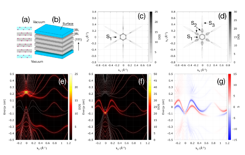
Bismuth has a rhombohedral Bravais lattice with two atoms per unit cell, forming a bilayer (BL) structure, as shown in Fig. 1(a). A Bi thin film is obtained by stacking the BLs along the (111) direction, such as the -axis depicted in Fig. 1(b). The surface is thus parallel to the plane. The uppermost and lowermost BLs are in contact with a vacuum.
We first construct a model Hamiltonian for the Bi thin film. For this purpose, the tight-binding model proposed for the bulk Bi crystal Liu and Allen (1995) is adapted to the Bi thin film. There are -, -, -, and -orbitals with spin index on each atom. The hopping terms among the atomic orbitals are decomposed into inter- and intra-BL hopping terms. The inter-BL hopping term consists of the nearest-neighbor hopping term in the bulk Bi Hamiltonian, whereas the intra-BL hopping term consists of two parts, and , with the third and second nearest-neighbor hopping terms in the bulk model, respectively. The Fermi energy is set to zero.
There is a surface potential gradient on the surface BL along the -axis between the surface Bi atoms and the vacuum. The surface Rashba effect is induced by the contribution of this potential gradient Petersen and Hedegård (2000); Ast and Gierz (2012). In terms of the tight-binding model, this is described by the following spin independent hopping terms between the nearest-neighbors sites, and Petersen and Hedegård (2000); Ast and Gierz (2012):
| (1) |
where is the azimuthal angle between and the -axis, and and are the hopping matrix elements of the Hamiltonian. Note that those hopping terms are zero in the bulk Bi crystal model because of the inversion symmetry. It is assumed that the surface hopping terms (1) appear only on the uppermost atomic layer, the first atomic layer of the uppermost BL, and the lowermost atomic layer with , because the surface field points in the opposite direction at the lowermost layer. The values of and remain to be determined at this stage.
The total Hamiltonian of the thin film is therefore represented by the following matrix form:
| (2) |
where is the Hamiltonian for the uppermost atomic layer, which includes the surface hopping terms (1) in addition to , while is the Hamiltonian that includes the surface hopping terms (1) with . The size of the matrix is thus when the number of the BLs is . The Hamiltonian (2) is a function of the wave vectors and : .
III Calculation of DOS
The DOS and the band structure of the thin film is obtained from the retarded Green’s function matrix with energy defined by
| (3) |
with in the numerical calculations. The DOS in the th BL is defined by
| (4) |
where represents the trace over the orbitals and the spin only on the th BL ( for the uppermost BL). In a similar way, the spin-resolved DOS is given by
| (5) |
where is the Pauli spin matrix that acts on the four orbital states. The eigenvalues of are also calculated to show the entire band structure of the film.
IV Parameter fitting
In the following, and are treated as fitting parameters. To fix these values, we use a phenomenological approach: We first calculate the DOS on the surface BL and the band structure for various values of and then compare them with the ARPES experimental results Ast and Höchst (2001); Koroteev et al. (2004); Hirahara et al. (2006, 2007a); Ohtsubo et al. (2012); Takayama et al. (2015) to find the best selection. This scheme was successful and led to , and . The numerical results appear similar near these values. Note that these values are the same order of magnitude as the hopping matrix elements between the second and third nearest neighbors given in Ref. Liu and Allen (1995).
The presence of the surface terms (1) is essential to explain the observed Fermi surface. Figures 1(c) and (d), show the DOS on the surface BL at the Fermi energy for the 16 BL thin film without and with the surface hopping terms, respectively. In both cases, a hexagonal electron pocket appears around the point designated by . Qualitative differences arise outside of ; with the surface hopping term, there are six hole lobes and six extra electron lobes, designated by , and , respectively, while is missing without the surface hopping term. The ARPES experiments show the presence of , which confirms that the surface terms (1) play a central role in the formation of the Fermi surface.
V Band structure
Next, we discuss the energy band structure along the - line (). Figures 1(e) and (f) show for the middle () and surface () BLs, respectively. The eigenvalues of are also shown as white lines for comparison. On the middle BL, the plot covers most of the eigenvalues, while on the surface BL, the plot appears only in a small fraction of the eigenvalue curves and mostly on two curves near the Fermi energy. The upper curve forms the and structures, whereas the lower curve forms the structure.
The spin-resolved band structure illustrates the distinctive features of the surface states, as shown in Fig 1(g). The spin splitting appears near the point, which is similar to Rashba spin splitting, and it diminishes near . This is consistent with the experimental results and the first-principles band calculations Hirahara et al. (2007b); Kimura et al. (2010). Thus, the surface states on the Bi film are well described by the phenomenological tight-binding model.
VI Surface spin states
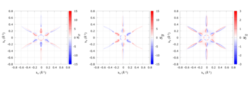
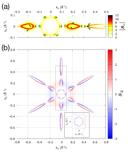
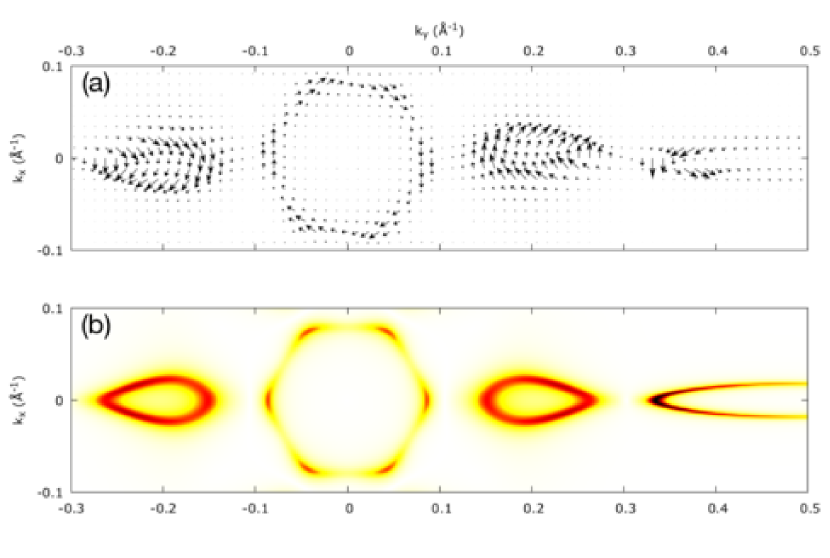
Next, we discuss the surface spin texture at the Fermi energy; . Figure 2(a) shows the in-plane spin distribution. On , lies along the pocket structure, while on , the direction of is opposite to that on . The in-plane spin rotations on and are broadly similar to those by the Rashba SOI. In addition, along the lobe on is almost constant. These observations are consistent with previous experimental results Kim et al. (2005); Hirahara et al. (2008); Takayama et al. (2011, 2014). However, the asymmetry of the along the axis on Takayama et al. (2011) is not observed in the present model. Instead of this asymmetry, on oscillates every 60∘. In addition, is not always perpendicular to on , which comes from the non-parabolic band structure. These indicate that the spin structure is not described by a simple Rashba SOI model.
The deviation from the simple Rashba model is clarified by the out-of-plane spin , as shown in Fig. 2(b). There is a relatively large over the – structures, where the maximum of is approximately 25 of the maximum of . Furthermore, changes its sign every 60∘. These results are consistent with recent experimental results Takayama et al. (2011), although larger values of are observed experimentally. In addition, the fine structure of is clarified, where the sign of also changes from to in the same manner as .
We further discuss the presence of the giant component. The first-principles calculations show similar results for with the topological phase of the Bi1-xSbx crystal Zhang et al. (2009), where is very small and around 1% of , which indicates the spin lies on the two-dimensional surface. Pure Bi () is in the trivial phase Fukui and Hatsugai (2007); Teo et al. (2008); Zhang et al. (2009); therefore, large values of may be direct evidence for clarification of the difference between the trivial and topological phases, besides the number of Fermi surface crossings from the zone center to the boundary. To support this point within the proposed model, without the surface hopping term near the point is shown in the inset of Fig. 2(b). Similar results are obtained both with and without the surface hopping terms. This indicates that the origin of is not from the surface effect, but from the bulk hopping terms and the atomic SOI of Bi itself, which determines the bulk band structure. Thus, the origin of for pure Bi is associated with the bulk band structure, which leads to a trivial phase.
VII BL number dependence
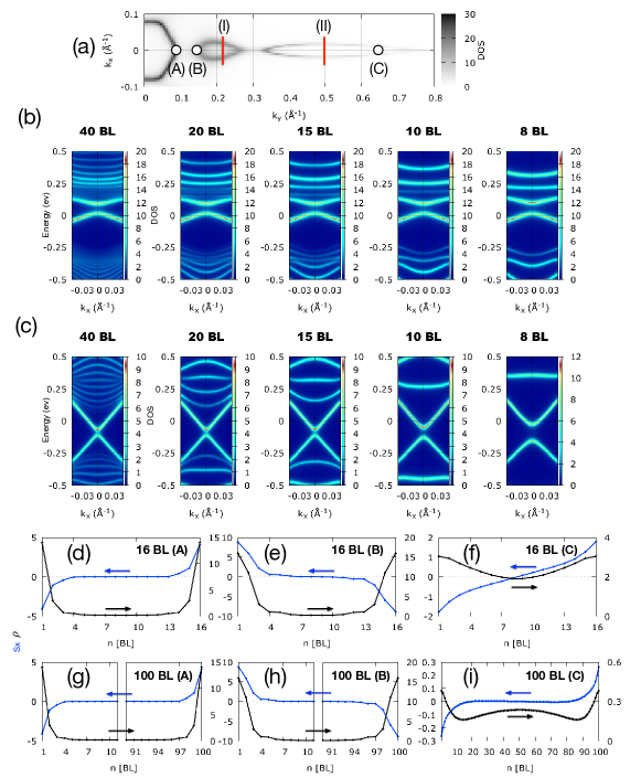
Figure 3(a) shows for a 40 BL film. Compared with that for the 16 BL film, both and structures are unchanged, while the structure is prolonged towards the point, which is consistent with the experimental results Hirahara et al. (2006, 2007a). To examine this difference in detail, we discuss the BL number dependence along the two lines and three points shown in Fig. 3(a).
Figure 3(b) shows in for various numbers of BLs along the line (I) shown in Fig. 3(a). The two surface states near the Fermi energy separated by a band gap are not affected by changing the BL number. However, the energy levels away from the Fermi level are under the strong influence of the BL number, which indicates the quantum confinement in the thin film. Figure 3(c) shows in along the line (II) shown in Fig. 3(a). Although the band structure near the Fermi level shows a linear dispersion similar to that for line (I), the band gap clearly decreases as the BL number increases. A similar observation is obtained experimentally Takayama et al. (2012). Hence, the surface states are under the strong influence of quantum confinement on , while they are not on .
Finally we discuss the surface state penetration inside the thin film. For this purpose, the layer-resolved DOS, and , are shown in Figs. 3(d-f) and (g-i) for the 16 BL and 100 BL films, respectively, at the three points indicated in Fig. 3(a). All the figures show that the spin on the uppermost and lowermost BLs are in opposite directions, as expected; The spin changes its sign at the middle of the film. The surface states on penetrate only a few BLs, and a similar result is obtained for the surface states on with a slightly longer penetration length. The penetration length is unchanged by the film thickness, which confirms they are genuine surface states. On other hand, at , and decay over 20 BLs, and is finite even at the middle of the film. Thus, the states are no longer simple “surface” states and are under the influence of the quantum confinement inside the film.
VIII Conclusions
We have shown that an tight-binding model with surface hopping terms can explain most of the experimental ARPES observations for bismuth thin films, including the Fermi surface, the spin-resolved band structure with Rashba spin splitting, and the quantum confinement effect in the energy band structure. The model also explains the large out-of-plane spin observed, which originates from the intrinsic Bi crystal structure rather than the surface effect. We have also clearly shown that the surface states penetrate inside the film to within approximately a few BLs near the Brillouin-zone center, whereas they reach the center of the film near the Brillouin-zone boundary.
The authors acknowledge A. Takayama for fruitful discussions and comments on the ARPES experimental results. We also thank J. Ieda for stimulating discussion. This work is partially supported by a Kakenhi Grant-in-Aid from the Ministry of Education, Culture, Sports, Science and Technology (MEXT) of Japan, and the Japan Science and Technology Agency (JST).
References
- Bychkov and Rashba (1984) Y. A. Bychkov and É. I. Rashba, JETP Lett. 39, 78 (1984).
- Winkler (2003) R. Winkler, Spin-orbit coupling effects in two-dimensional electron and hole systems, 191 (Springer Science & Business Media, 2003).
- LaShell et al. (1996) S. LaShell, B. A. McDougall, and E. Jensen, Phys. Rev. Lett. 77, 3419 (1996).
- Nicolay et al. (2001) G. Nicolay, F. Reinert, S. Hüfner, and P. Blaha, Phys. Rev. B 65, 033407 (2001).
- Henk et al. (2004) J. Henk, M. Hoesch, J. Osterwalder, A. Ernst, and P. Bruno, J. Phys. Condens. Matter 16, 7581 (2004).
- Hofmann (2006) P. Hofmann, Progress in Surface Science 81, 191 (2006).
- Ast and Höchst (2001) C. R. Ast and H. Höchst, Phys. Rev. Lett. 87, 177602 (2001).
- Koroteev et al. (2004) Y. M. Koroteev, G. Bihlmayer, J. E. Gayone, E. V. Chulkov, S. Blügel, P. M. Echenique, and P. Hofmann, Phys. Rev. Lett. 93, 046403 (2004).
- Kim et al. (2005) T. K. Kim, J. Wells, C. Kirkegaard, Z. Li, S. V. Hoffmann, J. E. Gayone, I. Fernandez-Torrente, P. Häberle, J. I. Pascual, K. T. Moore, A. J. Schwartz, H. He, J. C. H. Spence, K. H. Downing, S. Lazar, F. D. Tichelaar, S. V. Borisenko, M. Knupfer, and P. Hofmann, Phys. Rev. B 72, 085440 (2005).
- Hirahara et al. (2006) T. Hirahara, T. Nagao, I. Matsuda, G. Bihlmayer, E. V. Chulkov, Y. M. Koroteev, P. M. Echenique, M. Saito, and S. Hasegawa, Phys. Rev. Lett. 97, 146803 (2006).
- Hirahara et al. (2007a) T. Hirahara, T. Nagao, I. Matsuda, G. Bihlmayer, E. V. Chulkov, Y. M. Koroteev, and S. Hasegawa, Phys. Rev. B 75, 035422 (2007a).
- Hirahara et al. (2007b) T. Hirahara, K. Miyamoto, I. Matsuda, T. Kadono, A. Kimura, T. Nagao, G. Bihlmayer, E. V. Chulkov, S. Qiao, K. Shimada, H. Namatame, M. Taniguchi, and S. Hasegawa, Phys. Rev. B 76, 153305 (2007b).
- Hirahara et al. (2008) T. Hirahara, K. Miyamoto, A. Kimura, Y. Niinuma, G. Bihlmayer, E. V. Chulkov, T. Nagao, I. Matsuda, S. Qiao, K. Shimada, H. Namatame, M. Taniguchi, and S. Hasegawa, New Journal of Physics 10, 083038 (2008).
- Kimura et al. (2010) A. Kimura, E. E. Krasovskii, R. Nishimura, K. Miyamoto, T. Kadono, K. Kanomaru, E. V. Chulkov, G. Bihlmayer, K. Shimada, H. Namatame, and M. Taniguchi, Phys. Rev. Lett. 105, 076804 (2010).
- Takayama et al. (2011) A. Takayama, T. Sato, S. Souma, and T. Takahashi, Phys. Rev. Lett. 106, 166401 (2011).
- Ohtsubo et al. (2012) Y. Ohtsubo, J. Mauchain, J. Faure, E. Papalazarou, M. Marsi, P. Le Fèvre, F. Bertran, A. Taleb-Ibrahimi, and L. Perfetti, Phys. Rev. Lett. 109, 226404 (2012).
- Takayama et al. (2012) A. Takayama, T. Sato, S. Souma, T. Oguchi, and T. Takahashi, Nano Letters 12, 1776 (2012).
- Takayama et al. (2014) A. Takayama, T. Sato, S. Souma, and T. Takahashi, New J. Phys. 16, 055004 (2014).
- Takayama et al. (2015) A. Takayama, T. Sato, S. Souma, T. Oguchi, and T. Takahashi, Phys. Rev. Lett. 114, 066402 (2015).
- Hirahara et al. (2007) T. Hirahara, I. Matsuda, S. Yamazaki, N. Miyata, S. Hasegawa, and T. Nagao, Appl. Phys. Lett. 91, 202106 (2007).
- Jnawali et al. (2012) G. Jnawali, C. Klein, T. Wagner, H. Hattab, P. Zahl, D. P. Acharya, P. Sutter, A. Lorke, and M. Horn-von Hoegen, Phys. Rev. Lett. 108, 266804 (2012).
- Aitani et al. (2014) M. Aitani, T. Hirahara, S. Ichinokura, M. Hanaduka, D. Shin, and S. Hasegawa, Phys. Rev. Lett. 113, 206802 (2014).
- Hicks and Dresselhaus (1993a) L. D. Hicks and M. S. Dresselhaus, Phys. Rev. B 47, 12727 (1993a).
- Hicks and Dresselhaus (1993b) L. D. Hicks and M. S. Dresselhaus, Phys. Rev. B 47, 16631 (1993b).
- Hicks et al. (1993) L. D. Hicks, T. C. Harman, and M. S. Dresselhaus, Appl. Phys. Lett. 63, 3230 (1993).
- Murata et al. (2009) M. Murata, D. Nakamura, Y. Hasegawa, T. Komine, T. Taguchi, S. Nakamura, V. Jovovic, and J. P. Heremans, Appl. Phys. Lett. 94, 192104 (2009).
- Koroteev et al. (2008) Y. M. Koroteev, G. Bihlmayer, E. V. Chulkov, and S. Blügel, Phys. Rev. B 77, 045428 (2008).
- Liu and Allen (1995) Y. Liu and R. E. Allen, Phys. Rev. B 52, 1566 (1995).
- Fukui and Hatsugai (2007) T. Fukui and Y. Hatsugai, J. Phys. Soc. Jpn. 76, 053702 (2007).
- Teo et al. (2008) J. C. Y. Teo, L. Fu, and C. L. Kane, Phys. Rev. B 78, 045426 (2008).
- Murakami (2006) S. Murakami, Phys. Rev. Lett. 97, 236805 (2006).
- Petersen and Hedegård (2000) L. Petersen and P. Hedegård, Surface Science 459, 49 (2000).
- Ast and Gierz (2012) C. R. Ast and I. Gierz, Phys. Rev. B 86, 085105 (2012).
- (34) See Supplemental Material at http://link.aps.org/supplemental/ for the details of the magnitude and direction of the in-plane spin and surface spin DOS at the Fermi energy .
- Zhang et al. (2009) H.-J. Zhang, C.-X. Liu, X.-L. Qi, X.-Y. Deng, X. Dai, S.-C. Zhang, and Z. Fang, Phys. Rev. B 80, 085307 (2009).
Supplemental Material
Tight-binding theory of surface spin states on bismuth thin films
This supplemental material contains
-
•
Magnitude and direction of the in-plane spin,
-
•
Surface spin density of states (DOS) at the Fermi energy.
IX Magnitude and direction of the in-plane spin
Figure S1(a) shows the detailed magnitude and direction of and Fig. S1(b) shows a plot of for reference. The green arrows in Fig. 2(a) of the main text represent the directions of shown in Fig. S1(a) as representative points.
X Surface spin DOS at the Fermi energy
Figure S2 shows the surface spin DOS at the Fermi energy for all spin components.