Phosphorene and Transition Metal Dichalcogenide 2D Heterojunctions: Application in Excitonic Solar Cells
Abstract
Using the first-principles GW-Bethe-Salpeter equation method, here we study the excited-state properties, including quasi-particle band structures and optical spectra, of phosphorene, a two-dimensional (2D) atomic layer of black phosphorus. The quasi-particle band gap of monolayer phosphorene is 2.15 eV and its optical gap is 1.6 eV, which is suitable for excitonic thin film solar cell applications. Next, this potential application is analysed by considering type-II heterostructures with single layered phosphorene and transition metal dichalcogenides (TMDs). These heterojunctions have a potential maximum power conversion efficiency of up to 12%, which can be further enhanced to 20% by strain engineering. Our results show that phosphorene is not only a promising new material for use in nanoscale electronics, but also in optoelectronics.
I INTRODUCTION
The discovery of graphene in 2004 Novoselov et al. (2004) was a significant breakthrough in materials science and since then there has been sustained research interest in graphene and a rush to discover other stable two-dimensional (2D) materials. 2D materials have the thickness of one or a few atomic layers and have markedly different material properties than their bulk counterparts due to the quantum confinement effect. Since graphene, there have been several advances in the field of 2D materials such as the discovery of semiconducting monolayer transition metal dichalcogenides (TMDs) Mak et al. (2010); Wang et al. (2012). The growing number and variety of 2D materials has fuelled interest in the use of 2D materials in the development of novel nanoscale devices.
A recent development is the experimental isolation of a single layer of bulk black phosphorus, also known as phosphorene Brent et al. (2014); Buscema et al. (2014); Castellanos-Gomez et al. (2014); Li et al. (2014a); Liu et al. (2014); Qiao et al. (2014); Rodin et al. (2014); Zhu and Tománek (2014); Reich (2014); Churchill and Jarillo-Herrero (2014); Koenig et al. (2014); Fei and Yang (2014); Fei et al. (2015); Tran and Yang (2014); Tran et al. (2014); Guo et al. (2014); Peng et al. (2014); Peng and Wei (2014); Wang et al. (2015); Cai et al. (2014). Like graphene, phosphorene was first obtained by mechanical exfoliation Li et al. (2014a); Liu et al. (2014). Liquid exfoliation, which is a scalable process, has also been demonstrated as a possible alternative means of producing phosphorene Brent et al. (2014). Several experiments have demonstrated that phosphorene is a direct-gap semiconductor and also has a high hole mobilityLi et al. (2014a); Xia et al. (2014); Liu et al. (2014). These characteristics make phosphorene attractive for use in electronic and optoelectronic devices Xia et al. (2014). Field effect transistors (FET) based on few-layer phosphorene were shown to have high on/off ratios Li et al. (2014a). It also has the potential to be used as an anode material in lithium-ion batteries Li et al. (2015). Another potential application is in thin film excitonic solar cells as phosphorene has a predicted band gap in the visible region Dai and Zeng (2014). Excitonic solar cells (XSCs) based on some 2D materials, such as MoS2, WSe2, graphene, h-BN, SiC2 and bilayer phosphorene, are potentially seen as the new generation of thin film solar cellsTsai et al. (2014); Pospischil et al. (2014); Bernardi et al. (2012); Dai and Zeng (2014); Zhou et al. (2013); Britnell et al. (2013), and they might have higher efficiencies than existing XSCs which typically have less than 10% efficiency Green et al. (2015). Till now, despite the limitations of fabrication methodologies for such 2D solar cells, there has been some progress on the fabrication of few-layer heterostructures such as graphene-WS2Georgiou et al. (2012); Tan et al. (2014), graphene-MoS2Britnell et al. (2012) and phosphorene-MoS2Deng et al. (2014).
In this paper we study the excited-state properties of monolayer phosphorene, and evaluate the viability of monolayer phosphorene as one building block of of an excitonic solar cell heterostructure. For the other building-block material in the heterostructure, the semiconducting monolayer TMDs, which have been extensively researched, are chosen. The semiconducting TMDs considered here include semiconducting MoS2, MoSe2, MoTe2, WS2, WSe2, WTe2, TiS2 and ZrS2. This paper is organized as follows: In Sec. II, we first introduce the structures of geometrically optimized monolayer phosphorene and computational details. Sec. III is the main part of results and discussions, which includes three subsections: In SubSec. A, we show the excited-state properties of monolayer phosphorene, including in quasi-particle band structures and optical spectra. In SubSec. B, we calculate the excited-state properties of 8 semiconducting TMDs. In SubSec. C, the band alignment of phosphorene and TMDs is presented. Then the power conversion efficiencies (PCE) of the phosphorene-TMD heterostructures are discussed. In Sec. IV, we conclude our studies.
II Structures and COMPUTATIONAL DETAILS
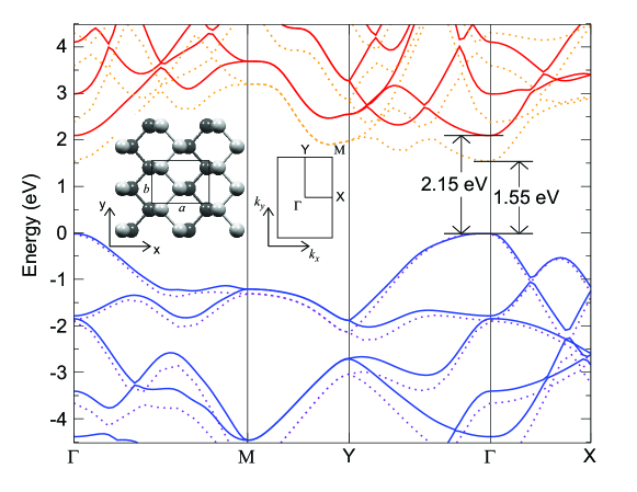
Phosphorene has a puckered honeycomb structure as shown in inset of Figure 1. The underlying lattice is rectangular which leads to anisotropy in the band structure and optical properties. The calculated lattice constants are Å and Å which are consistent with results in literature Liu et al. (2014). The calculations were performed using the Vienna Ab-initio Simulation Package (VASP) Kresse and Furthmüller (1996a, b); Kresse and Hafner (1993, 1994), and a projector augmented wave (PAW) basis set was used Blöchl (1994); Kresse and Joubert (1999). Geometry optimisation was done using density function theory (DFT) with the generalised gradient approximation (GGA) using the Perdew-Burke-Ernzerhof (PBE) exchange correlation functional. A -point grid was used for phosphorene while an -point grid was used for TMDs. The geometry was relaxed until the force acting on the atoms was less than 0.01 eV/atom. To ensure that the interlayer interaction is negligible, the out of plane lattice parameter, which is perpendicular to the plane of the material, was set as at least 15 Å. Band gaps and band structures were calculated using the GW method. The band gaps/structures were also calculated through the screened exchange hybrid density functional by Heyd, Scuseria, and Ernzerhof (HSE06) for reference. A high number of empty conductions bands is necessary for the convergence of the absolute band positionsLiang et al. (2013). A total of 1024 bands were used for phosphorene and 1536 bands were used for TMDs. Single shot GW calculations, , were performed on phosphorene to obtain the ground state band energies. For TMDs, one eigenvalue update is performed to obtain the expected direct band gap of trigonal prismatic TMDs Shi et al. (2013); Cheiwchanchamnangij and Lambrecht (2012); Ramasubramaniam (2012); Qiu et al. (2013). The band structure was then interpolated from Wannier functions rather than evaluated directly at discrete -points. This was done using the WANNIER90 library Mostofi et al. (2008) and the VASP2WANNIER interface. The optical gap was calculated by solving the Bethe-Salpeter equation (BSE). The GW method has more computational demands and the band gaps converge with a much smaller number of bandsLiang et al. (2013). Thus to streamline optical calculations, the calculation was run with 128 bands for phosphorene and 192 bands for TMDs before solving the BSE. This produced the frequency dependent dielectric tensor that was used to calculate the absorption spectrum. By solving the BSE, electron-hole interactions such as excitons are accounted for in the dielectric tensor. For phosphorene the - and -components of the dielectric tensor were treated separately because of the anisotropy but for TMDs, the average value of the - and -components was used due to crystal symmetry.
III RESULTS AND DISCUSSIONS
III.1 Excited-state properties of phosphorene
The calculated band structure of phosphorene is shown in Figure 1. The GW calculation predicts a band gap value of 2.15 eV and the gap is approximately located at the point, which is much higher than the DFT-calculated band gap of 0.91 eV Qiao et al. (2014). The conduction band minimum (CBM) and the valence band maximum (VBM) are not exactly aligned in the GW-calculated band structure, but they are sufficiently close to be considered as a direct band gap Tran et al. (2014). A similar computational approach by Tran et al. predicted a band gap of 2.0 eV and a comparable profile of the band structure Tran et al. (2014). The CBM position is around -4.25 eV with respect the the vacuum level. Besides the GW method, the hybrid density functional HSE06 was used to calculate the band structures and band gap for reference in Fig. 1. As can be seen, the HSE06-calculated band gap is 0.6 eV lower than the GW-calculated gap, which is in agreement with previous calculations Qiao et al. (2014).
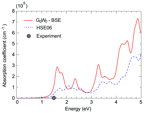
The optical gap of phosphorene is calculated using the GW-BSE approach and is determined to be 1.6 eV. This is the first optical peak of the absorption spectrum for light polarised along the armchair direction as seen in Fig. 2. This optical gap is slightly larger than the experimental photoluminescence measurement value of 1.45 eV of phosphorene Liu et al. (2014), but smaller than the HSE06-calculated value of 1.8 eV. The optical gap of 1.6 eV is much lower than the electronic band gap of 2.15 eV which suggests that significant excitonic effects are present in phosphorene. The exciton binding energy of 0.55 eV in monolayer phosphorene is quite huge. Both the self-energy corrected large electronic gap and small optical gap of phosphorene indicate significant many-electron effect in phosphorene.
III.2 Excited-state properties of TMDs
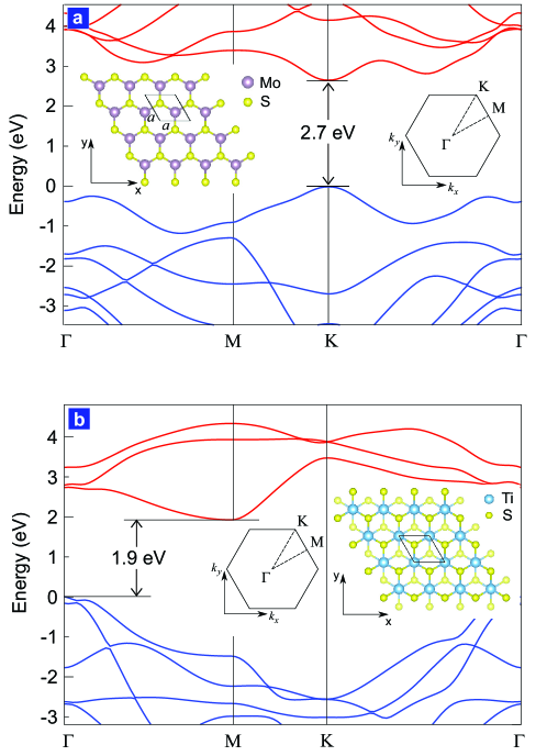
Using a similar approach to the above, the geometry, band positions and band structures of 8 semiconducting TMDs are calculated. A summary of the lattice constants, absolute positions of the valence band maximum (VBM) and conduction band minimum for the different materials is shown in Table 1. The TMDs are categorised into either trigonal prismatic or octahedral TMDs, both of which have a hexagonal lattice but different coordination of the atoms within the unit cell. The two different structures are shown in the inset of Fig. 3. For trigonal prismatic TMDs, the lattice constant is largely determined by the size chalcogen atom which increases with atomic number (sulphur to selenium to tellurium). Furthermore, as can be seen, phosphorene has a large exciton binding energy compared to TMDs because of its unique quasi 1D band dispersions.
| Material | Lattice | Structure | (Å) | (Å) | (eV) | (eV) | (eV) | (eV) |
|---|---|---|---|---|---|---|---|---|
| Phosphorene | Rectangular | - | 4.58 | 3.30 | 2.15 | -6.40 | -4.25 | 1.6 |
| MoS2 | Hexagonal | Trigonal Prismatic | 3.16 | - | 2.68 | -6.57 | -3.89 | 2.3 |
| MoSe2 | Hexagonal | Trigonal Prismatic | 3.29 | - | 2.39 | -5.97 | -3.58 | 2.2 |
| MoTe2 | Hexagonal | Trigonal Prismatic | 3.52 | - | 1.74 | -5.43 | -3.69 | 1.7 |
| WS2 | Hexagonal | Trigonal Prismatic | 3.16 | - | 2.94 | -6.47 | -3.53 | 2.5 |
| WSe2 | Hexagonal | Trigonal Prismatic | 3.26 | - | 2.70 | -5.84 | -3.14 | 2.6 |
| WTe2 | Hexagonal | Trigonal Prismatic | 3.52 | - | 1.98 | -5.35 | -3.37 | 1.9 |
| TiS2 | Hexagonal | Octahedral | 3.37 | - | 1.88 | -6.80 | -4.88 | - |
| ZrS2 | Hexagonal | Octahedral | 3.58 | - | 2.65 | -7.56 | -4.81 | - |
The trigonal prismatic TMDs have a direct band gap the the point [see Supplementary Materials]. They have the similar band structures. The band structure of MoS2 is shown in Fig. 3(a) as an example. For trigonal prismatic TMDs, the band gap decreases with increasing chalcogen atomic number. The CBM position also decreases with increasing chalcogen atomic number. These trends and the band gap values are consistent with other similar studies of these materials Gong et al. (2013); Liang et al. (2013); Kang et al. (2013); Ding et al. (2011); Shi et al. (2013). Octahedral TMDs have an indirect band gap between the and points [see Supplementary Materials]. This is also in agreement with band profiles calculated in previous studies. Liang et al. (2013); Gong et al. (2013); Ivanovskaya (2005); Li et al. (2014b); Kang et al. (2013); Jiang (2012). The band structure of TiS2 is shown in Figure 3(b).
III.3 Band offset and PCE of excitonic solar cells
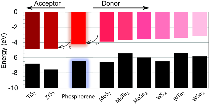
Note that many important properties and potential device applications of semiconductors are not determined entirely by the band gap only. The band alignment and corresponding band offsets (the relative band-edge energies) of two or more semiconductors are other fundamental/critical parameters in the design of heterojunction devices Wei and Zunger (1998); Zhang et al. (2000); Jiang (2012); Kang et al. (2013); Liang et al. (2013), for example, the 2D heterostructure devices for photocatalytic water splitting Jiang (2012); Kang et al. (2013); Liang et al. (2013), field effect transistors Gong et al. (2013) and p-n diodesDeng et al. (2014). Chemical trends of the band offesets provide a useful tool for predicting catalytic ability of TMDs-based heterojunctions. Figure 4 shows the band alignment (using the vacuum level as reference) of phosphorene with 8 semiconducting monolayer TMDs. It can be seen that the CBM of trigonal prismatic TMDs is higher than that of monolayer phosphorene, while the CBM of octahedral TMDs is lower than phosphorene. Thus, trigonal prismatic TMDs could function as the donor whereas octahedral TMDs would function as the acceptor in heterostructure with phosphorene. The optical gap of 8 TMDs is calculated, which is determined from the absorption spectrum. In most cases, the optical gap is slightly lower than the electronic band gap as shown in Table 1. Notice that because of strong many-electron effects in some 2D materials, such as phosphorene and MoS2, we might not get the accurate band offset parameters in some cases without considering the excited-state effect. For example, the HSE-calculated CBM band energy of monolayer MoS2 is -4.21 eV Guo et al. (2014) (-4.25 eV Kang et al. (2013)) and phosphorene is -3.94 eV Guo et al. (2014) (-3.92 eV Cai et al. (2014)). Thus, phoshporene (MoS2) is the donor (acceptor) in the phosphorene-MoS2 2D heterojunction Guo et al. (2014) and the predicted PCE is 17.5% Guo et al. (2014). However, if we consider many-electron effects, the GW-calculated CBM band energy of monolayer MoS2 is -3.89 eV (-3.74 eV Liang et al. (2013)) and phosphorene is -4.25 eV. Interestingly, phoshporene (MoS2) becomes the acceptor (donor) instead and the predicted PCE is reducing to 10%. Regarding to other 2D materials without strong many-electron effects, both HSE and GW can give similar band offset Liang et al. (2013); Kang et al. (2013).
A model developed by Scharber et al. for organic solar cells Scharber et al. (2006) and later adapted for exciton based 2D solar cells Bernardi et al. (2012); Dai and Zeng (2014) is used to predict the maximum PCE, , based on the fill-factor, , open circuit voltage, , and short circuit current, .
| (1) |
where is the total incident solar power per unit area based on the Air Mass (AM) 1.5 solar spectrum ASTM G173-03 (2012); Renewable Resource Data Centre (2014). The fill factor is the ratio of power output at the maximum power point to the product of the open circuit voltage and the short circuit current. The fill factor is estimated to be from literature. The , in units of V, and , in units of A/, are estimated in the limit of 100% external quantum efficiency as
| (2) | ||||
| (3) |
where is the elementary charge, is the donor optical gap, is the conduction band offset and is AM 1.5 solar spectrum. In equation 2, the constant 0.3 eV is an empirical parameter that estimates losses due to energy conversion kinetics.
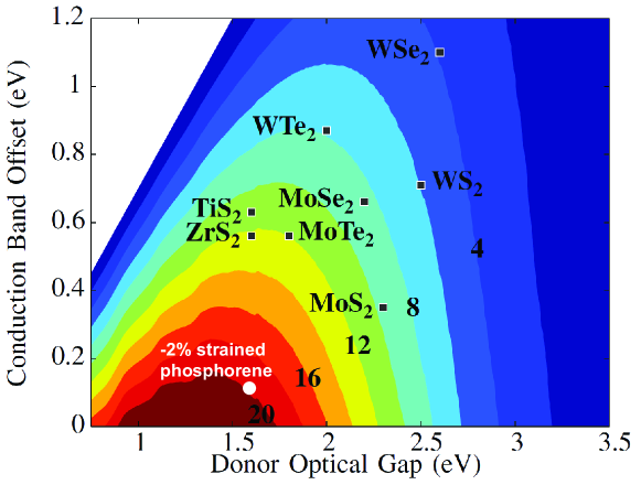
Using this model the TMDs are paired with phosphorene. The material with the lower CBM is the acceptor and the material with the higher CBM is the donor. Phosphorene is the donor when paired with both octahedral TMDs and the acceptor when paired with trigonal prismatic TMDs. The maximum PCE values for these eight heterostructures are marked on Fig. 5. Of the eight heterostructures, phosphorene-ZrS2 and MoTe2-phosphorene have the highest PCE value of 12%. This efficiency is higher than that achieved by existing excitonic solar cells, and comparable to the proposed 2D g-SiC2/GaN (14.2%), PCBM/CBN (10-20%)Bernardi et al. (2012), and bilayer-phosphorene/MoS2 (16-18%) solar cells.
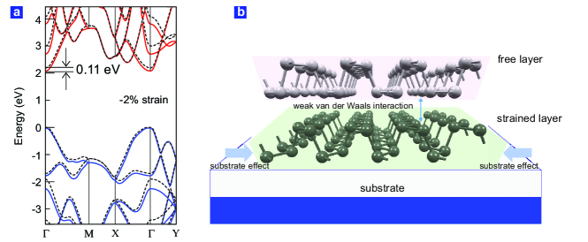
Actually, a further observation based on this model is that a solar cell with a phosphorene donor could have maximum PCE values of up to about 20% with an appropriate choice for the acceptor. The conduction band offset (CBO) between phosphorene and TiS2 is 0.63 eV while the CBO between phosphorene and ZrS2 is 0.56 eV for the two cases here where monolayer phosphorene is the donor. This translates to a significant drop in in the model which results in a lower PCE. In addition to looking out for new materials that have a better band alignment with phosphorene, means of tuning the properties of both the donor and acceptor can be considered. For example, strained phosphorene may be used as the acceptor material because the strain effect is a well-known method to tune the band structure of materials Fei and Yang (2014); Fei et al. (2015). The band structures of different strained monolayer phosphorene are shown in Supplementary Materials. Here, we choose the phosphorene with 2% compressed strain (along the armchair direction) as a donor. Its band structure is shown in Fig. 6. For comparison, the band structure of phosphorene without strain is also presented in the same figure. As can be seen, the position of CMB can be effectively tuned by the strain effect. 2% compressed armchair strain can shift the CBM down to the Fermi level around 0.11 eV because the compressed strain enhances the interaction of hybridized orbitals of P atoms, which contribute to the CBM. The calculated PCE value of -2% strained-phosphorene/phosphorene can be around 20% as shown by the white solid circle in Fig. 5. Based on the theoretical studies of mechanical properties of monolayer phosphorene, the mechanical stability of phosphorene can be up to under 30% strain Wei and Peng (2014); Peng et al. (2014). The 2% compressed strain of a monolayer phorphorene can be realized by the substrate effect in the experiment [see Fig. 6(b)]. Meanwhile, there is no strain on the second deposited monolayer phosphorene because of the weak van der Waals interaction between the two phosphorene layers. This can realize the strain/non-strain phosphorene heterostructure.
Alternatively multilayer structures of phosphorene or TMDs may also be considered to increase the overall power conversion per unit area. Our calculated optical gap of phosphorene is 1.6 eV which is at the edge of the infrared region. Therefore, heterostructures with a phosphorene donor may be considered for multijunction solar cells absorbing photons across the entire visible spectrum. Such cells incorporate several junctions that aim to absorb different portions of the solar spectrum so as to maximise total absorption [See Supplementary Materials]. Given the anisotropy of phosphorene, the stacking orientation in multilayer structures may be a significant factor Dai and Zeng (2014).
IV CONCLUSIONS
In conclusion, through GW calculations, the band structures and optical spectra of monolayer phosphorene have been calculated. The electronic gap of 2.15 eV and the optical gap of 1.6 eV are desirable for solar cell applications because of the strong exciton binding energy. When paired with ZrS2 or MoTe2 the power conversion efficiency of the excitonic solar cells can be as high as 12%. There is further potential to improve the PCE of phosphorene based solar cells substantially by tuning the materials, such as through the strain and multi-stacking effect, to achieve a better band alignment.
V ACKNOWLEDGEMENT
Authors thank Minggang Zeng for his helpful discussion. This project was supported by the Computational Condensed Matter Physics Laboratory, NUS. Computational resources were provided by Centre for Advanced 2D Materials, NUS.
References
- Novoselov et al. (2004) K. S. Novoselov, A. K. Geim, S. V. Morozov, D. Jian, Y. Zhang, S. V. Dubonos, I. V. Grigorieva, and A. A. Firsov, Science 306, 666 (2004).
- Mak et al. (2010) K. F. Mak, C. Lee, J. Hone, J. Shan, and T. F. Heinz, Phys. Rev. Lett. 105, 136805 (2010).
- Wang et al. (2012) Q. H. Wang, K. Kalantar-Zadeh, A. Kis, J. N. Coleman, and M. S. Strano, Nat. Nanotech. 7, 699 (2012).
- Brent et al. (2014) J. R. Brent, N. Savjani, E. A. Lewis, S. J. Haigh, D. J. Lewis, and P. O’Brien, Chem. Commun. 50, 13338 (2014).
- Buscema et al. (2014) M. Buscema, D. J. Groenendijk, G. A. Steele, H. S. van der Zant, and A. Castellanos-Gomez, Nat. Commun. 5, 4651 (2014).
- Castellanos-Gomez et al. (2014) A. Castellanos-Gomez, L. Vicarelli, E. Prada, J. O. Island, K. L. Narasimha-Acharya, S. I. Blanter, D. J. Groenendijk, M. Buscema, G. A. Steele, J. V. Alvarez, H. W. Zandbergen, J. J. Palacios, and H. S. J. van der Zant, 2D Mater. 1, 025001 (2014).
- Li et al. (2014a) L. Li, Y. Yu, G. J. Ye, Q. Ge, X. Ou, H. Wu, D. Feng, X. H. Chen, and Y. Zhang, Nat. Nanotechnol. 9, 372 (2014a).
- Liu et al. (2014) H. Liu, A. T. Neal, Z. Zhu, Z. Luo, X. Xu, D. Tománek, and P. D. Ye, Acs Nano 8, 4033 (2014).
- Qiao et al. (2014) J. Qiao, X. Kong, Z.-X. Hu, F. Yang, and W. Ji, Nat. Commun. 5, 4475 (2014).
- Rodin et al. (2014) A. S. Rodin, A. Carvalho, and A. H. Castro Neto, Phys. Rev. Lett. 112, 176801 (2014).
- Zhu and Tománek (2014) Z. Zhu and D. Tománek, Phys. Rev. Lett. 112, 176802 (2014).
- Reich (2014) E. S. Reich, Nature 506, 19 (2014).
- Churchill and Jarillo-Herrero (2014) H. O. Churchill and P. Jarillo-Herrero, Nat. Nanotechnol. 9, 330 (2014).
- Koenig et al. (2014) S. P. Koenig, R. A. Doganov, H. Schmidt, A. H. Castro Neto, and B. Oezyilmaz, Appl. Phys. Lett. 104, 103106 (2014).
- Fei and Yang (2014) R. Fei and L. Yang, Nano. Lett. 14, 2884 (2014).
- Fei et al. (2015) R. Fei, V. Tran, and L. Yang, Phys. Rev. B 91, 195319 (2015).
- Tran and Yang (2014) V. Tran and L. Yang, Phys. Rev. B 89, 245407 (2014).
- Tran et al. (2014) V. Tran, R. Soklaski, Y. Liang, and L. Yang, Phys. Rev. B 89, 235319 (2014).
- Guo et al. (2014) H. Guo, N. Lu, J. Dai, X. Wu, and X. C. Zeng, J. Phys. Chem. C 118, 14051 (2014).
- Peng et al. (2014) X. Peng, Q. Wei, and A. Copple, Phys. Rev. B 90, 085402 (2014).
- Peng and Wei (2014) X. Peng and Q. Wei, Mater. Res. Express 1, 045041 (2014).
- Wang et al. (2015) V. Wang, Y. Kawazoe, and W. Geng, Phys. Rev. B 91, 045433 (2015).
- Cai et al. (2014) Y. Cai, G. Zhang, and Y.-W. Zhang, Sci. Rep. 4, 6677 (2014).
- Xia et al. (2014) F. Xia, H. Wang, and Y. Jia, Nat. Commun. 5, 5458 (2014).
- Li et al. (2015) W. Li, Y. Yang, G. Zhang, and Y.-W. Zhang, Nano Lett. 15, 1691 (2015).
- Dai and Zeng (2014) J. Dai and X. C. Zeng, J. Phys. Chem. Lett. 5, 1289 (2014).
- Tsai et al. (2014) M.-L. Tsai, S.-H. Su, J.-K. Chang, D.-S. Tsai, C.-H. Chen, C.-I. Wu, L.-J. Li, L.-J. Chen, and J.-H. He, ACS Nano 8, 8317 (2014).
- Pospischil et al. (2014) A. Pospischil, M. M. Furchi, and T. Mueller, Nat. Nanotech. 9, 257 (2014).
- Bernardi et al. (2012) M. Bernardi, M. Palummo, and J. C. Grossman, ACS Nano 6, 10082 (2012).
- Zhou et al. (2013) L.-J. Zhou, Y.-F. Zhang, and L.-M. Wu, Nano letters 13, 5431 (2013).
- Britnell et al. (2013) L. Britnell, R. Ribeiro, A. Eckmann, R. Jalil, B. Belle, A. Mishchenko, Y.-J. Kim, R. Gorbachev, T. Georgiou, S. Morozov, A. Grigorenko, A. Geim, C. Casiraghi, A. H. Castro Neto, and K. Novoselov, Science 340, 1311 (2013).
- Green et al. (2015) M. A. Green, K. Emery, Y. Hishikawa, W. Warta, and E. D. Dunlop, Progress in Photovoltaics: Research and Applications 23, 1 (2015).
- Georgiou et al. (2012) T. Georgiou, R. Jalil, B. D. Belle, L. Britnell, R. V. Gorbachev, S. V. Morozov, Y.-J. Kim, A. Gholinia, S. J. Haigh, O. Makarovsky, L. Eaves, L. A. Ponomarenko, A. K. Geim, K. S. Novoselov, and A. Mishchenko, Nat. Nanotech. 8, 100 (2012).
- Tan et al. (2014) J. Y. Tan, A. Avsar, J. Balakrishnan, G. K. W. Koon, T. Taychatanapat, E. C. T. O’Farrell, K. Watanabe, T. Taniguchi, G. Eda, and A. H. Castro Neto, Appl. Phys. Lett. 104, 183504 (2014).
- Britnell et al. (2012) L. Britnell, R. Gorbachev, R. Jalil, B. Belle, F. Schedin, A. Mishchenko, T. Georgiou, M. Katsnelson, L. Eaves, S. Morozov, A. Grigorenko, A. Geim, C. Casiraghi, A. Neto, and K. Novoselov, Science 335, 947 (2012).
- Deng et al. (2014) Y. Deng, Z. Luo, N. J. Conrad, H. Liu, Y. Gong, S. Najmaei, P. M. Ajayan, J. Lou, X. Xu, and P. D. Ye, ACS Nano 8, 8292 (2014).
- Kresse and Furthmüller (1996a) G. Kresse and J. Furthmüller, Phys. Rev. B 54, 11169 (1996a).
- Kresse and Furthmüller (1996b) G. Kresse and J. Furthmüller, Comp. Mater. Sci. 6, 15 (1996b).
- Kresse and Hafner (1993) G. Kresse and J. Hafner, Phys. Rev. B 47, 558 (1993).
- Kresse and Hafner (1994) G. Kresse and J. Hafner, Phys. Rev. B 49, 14251 (1994).
- Blöchl (1994) P. E. Blöchl, Phys. Rev. B 50, 17953 (1994).
- Kresse and Joubert (1999) G. Kresse and D. Joubert, Phys. Rev. B 59, 1758 (1999).
- Liang et al. (2013) Y. Liang, S. Huang, R. Soklaski, and L. Yang, Appl. Phys. Lett. 103, 042106 (2013).
- Shi et al. (2013) H. Shi, H. Pan, Y.-W. Zhang, and B. I. Yakobson, Phys. Rev. B 87, 155304 (2013).
- Cheiwchanchamnangij and Lambrecht (2012) T. Cheiwchanchamnangij and W. R. Lambrecht, Phys. Rev. B 85, 205302 (2012).
- Ramasubramaniam (2012) A. Ramasubramaniam, Phys. Rev. B 86, 115409 (2012).
- Qiu et al. (2013) D. Y. Qiu, H. Felipe, and S. G. Louie, Phys. Rev. Lett. 111, 216805 (2013).
- Mostofi et al. (2008) A. A. Mostofi, J. R. Yates, Y.-S. Lee, I. Souza, D. Vanderbilt, and N. Marzari, Comp. Phys. Commun. 178, 685 (2008).
- Gong et al. (2013) C. Gong, H. Zhang, W. Wang, L. Colombo, R. M. Wallace, and K. Cho, Appl. Phys. Lett. 103, 053513 (2013).
- Kang et al. (2013) J. Kang, S. Tongay, J. Zhou, J. Li, and J. Wu, Appl. Phys. Lett. 102, 012111 (2013).
- Ding et al. (2011) Y. Ding, Y. Wang, J. Ni, L. Shi, S. Shi, and W. Tang, Phys. B: Cond. Matt. 406, 2254 (2011).
- Ivanovskaya (2005) V. V. Ivanovskaya, Semiconductors 39, 1058 (2005).
- Li et al. (2014b) Y. Li, J. Kang, and J. Li, RSC Advances 4, 7396 (2014b).
- Jiang (2012) H. Jiang, J. Phys. Chem. C 116, 7664 (2012).
- Wei and Zunger (1998) S.-H. Wei and A. Zunger, Appl. Phys. Lett. 72, 2011 (1998).
- Zhang et al. (2000) S. Zhang, S.-H. Wei, and A. Zunger, Phys. Rev. Lett. 84, 1232 (2000).
- Scharber et al. (2006) M. C. Scharber, D. Mühlbacher, M. Koppe, P. Denk, C. Waldauf, A. J. Heeger, and C. J. Brabec, Adv. Mater. 18, 789 (2006).
- ASTM G173-03 (2012) ASTM G173-03, “Standard tables for reference solar spectral irradiances: Direct normal and hemispherical on 37∘ tilted surface,” (2012).
- Renewable Resource Data Centre (2014) Renewable Resource Data Centre, “Solar spectral irradiance: Air mass 1.5,” (2014).
- Wei and Peng (2014) Q. Wei and X. Peng, Appl. Phys. Lett. 104, 251915 (2014).