Light Emission in Silicon from Carbon Nanotubes
Abstract
The use of optics in microelectronic circuits to overcome the limitation of metallic interconnects is more and more considered as a viable solution. Among future silicon compatible materials, carbon nanotubes are promising candidates thanks to their ability to emit, modulate and detect light in the wavelength range of silicon transparency. We report the first integration of carbon nanotubes with silicon waveguides, successfully coupling their emission and absorption properties. A complete study of this coupling between carbon nanotubes and silicon waveguides was carried out, which led to the demonstration of the temperature-independent emission from carbon nanotubes in silicon at a wavelength of 1.3 m. This represents the first milestone in the development of photonics based on carbon nanotubes on silicon.
Keywords: nanotube, photonics, silicon, photoluminescence
keywords:
nanotube, photonics, silicon, photoluminescenceCurrent address: Martel group, Univ. Montréal, Montréal, Canada
Enhancing microprocessor performances is becoming increasingly more complex. This complexity stems from the rising transistor count and the transistor’s shrinking size in the quest to follow Moore’s Law1. As a consequence, power consumption in microprocessor increases, and the on-chip communication between differents components becomes more and more difficult, and is even now a key-point for future multi-core generations2. To overcome these problems, one of the most promising solutions is the use of optical interconnects, which combine high data rate transmission, low power consumption, synchronization and crosstalk3, 4. In recent years, silicon photonics was extensively studied for the realisation of high-speed optical links5, 6, 7. Nowadays, compact photonic structures are achieved due to the strong refractive index contrast between silicon and silica and low loss optical propagation in the wavelengths range from 1.25 m to 1.65 m. In particular, various passive devices for wavelength multiplexing or light distribution (90∘ bends…) are easily feasible with silicon photonics technology8, 9.
Nevertheless, silicon is an indirect bandgap material, and its optoelectronic properties are insufficient to generate light and not sensitive enough to detect the flux of photons transmitted in an optical link. Other materials, such as III-V semiconductors, are good alternatives for light emission10, 11, while germanium could realize high speed photodetectors12, 13. Silicon is still used for efficient and high speed optical modulators14. The integration of all these materials on silicon is technically possible, but as different and sometimes non-compatible process are used, the resulting scheme is not cost-effective, and consequently reduce the use of silicon photonics for a broad application domain. A monolithic integration of laser source, optical modulator, and photodetector with a common material would be much more favorable for emergence of photonics.
We envision the use of carbon nanotubes for all active optoelectronic devices in silicon in order to avoid these non compatible processes. Carbon nanotubes (SWNT) are a very versatile material, presenting at the same time very good electronic properties15, and also optical properties16, 17, 18. They display strong photo- and electro-luminescence, in the 1-2 m wavelength range19, 20, 21, 22, and the emission could be tuned by selecting a precise nanotube diameter and chirality23. The possibility to use electrical pumping for luminescence generation is extremely interesting for the realization of electrically pumped optical laser24, 25. Recent works revealed that SWNT displays electroabsorption properties, which could be used to achieve optical modulation26, 27. Finally, nanotubes present various absorption bands in the 1-2 m range, allowing realization of photodetectors28, 29. Therefore, carbon nanotubes are very good candidates to solve integration issues in silicon photonics, and make cost-effective and reliable photonics. Moreover, a side advantage of the use of nanotubes for photonics is that the current research on the use of nanotube for nanoelectronics30 will facilitate the integration between photonics and electronics.
In this paper, we propose a way to integrate nanotubes with silicon photonics technology, which is a key-point for future realisation of carbon nanotube based photonic devices. This work looks into the difficulties of coupling the optical properties of a 1D nanomaterial (SWNT) to a bulk 3D material like silicon. In this context, we report the first integration of nanotubes’ absorption and emission properties in silicon waveguides at telecommunication wavelengths around 1.3 m.
1 Results and discussions
1.1 Integration scheme design
The integration scheme considered is based on the insertion of an interacting zone in an input/output silicon waveguide. It is constituted of a sub-micron silicon waveguide embedded in a carbon nanotubes composite, as schematically presented in Fig. 1. The input and output waveguides have both a width of 450 nm. For such geometry, the optical mode is strongly confined into the waveguide (Fig. 1A) due to the high refractive index contrast between silicon (optical index 3.45) and its top and bottom cladding layers where the index is near 1.45. This confinement prevents strong interactions with the surrounding media, allowing high transmission of optical signal. On the other hand, the waveguide in the interaction region with carbon nanotubes has a width below the critical minimum confinement width , which is the limit under a significant fraction of the optical mode starts to leak outside the silicon waveguide. At 1.3 m, is around 400 nm. A judicious shrinkage of the waveguide width allows both deconfining a controlled fraction of the optical mode and preserving the propagation of the optical wave along the waveguide. Fig. 1B illustrates the mode confinement calculated for a of 275 nm and shows the optical mode spreading outside the waveguide silicon core. As a significant fraction of the energy is propagating outside the waveguide, the guided mode will have a strong interaction with the active SWNT based polymer top cladding layer. To minimize optical losses in the transition between the input/output waveguide ( = 450 nm) and the interaction region waveguide ( = 275 nm), adiabatic tapers are required (typically 300 m long).
1.2 Technology
The substrate is a silicon-on-insulator (SOI) with a 220 nm thick silicon layer on top of a 1 m thick buried silica layer. Although details of the technological steps are given in supporting information, briefly, silicon waveguides were made using e-beam lithography patterning followed by reactive ion plasma etching (RIE). A 500 nm thick silicon dioxide (\ceSiO2) protection layer was deposited onto the silicon wafer using a plasma-enhanced chemical vapor deposition (PECVD) technique. A silica recess of length corresponding to the interaction region was etched down to the buried silicon oxide layer in order to expose the vicinity of the waveguide allowing interactions with the surrounding medium, and in particular SWNT. (1C).
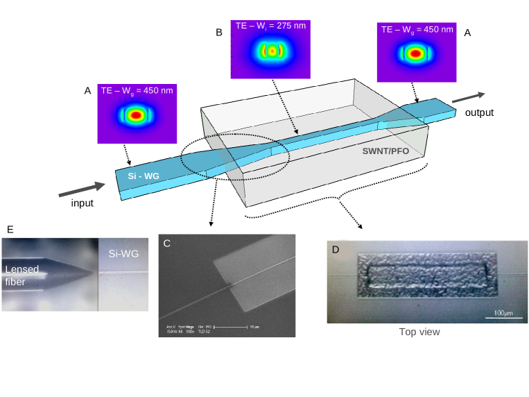
The single-wall carbon nanotube (SWNT) film was prepared as follow: as-prepared HiPCO SWNT powder (Unydim Inc.) were mixed with poly-9,9-di-n-octyl-fluorenyl-2,7-diyl (PFO) in toluene at a ratio of SWNT (5 mg): PFO (5 mg): toluene (30 ml). This mixture was homogenized by sonication (for 1 h using a water-bath sonicator and 15 min using a tip sonicator) and was centrifuged for 5-60 min using a desktop centrifuge (angle rotor type, 10,000 g). Solution was then drop casted directly into the previously defined silica recess to form a 1 m thick layer. Samples were further annealed at 180∘C for 15 min to improve optical quality of the SWNT/PFO film19, 31. This layer was then delimited around the interaction region by another \ceO2-based RIE to remove the SWNT/PFO film on the undesired areas (1D).

The evolution of the optical mode fraction confined in the SWNT/PFO layer (filling factor ) was determined as a function of the waveguide width by mode-solving numerical simulations using an home-made simulation code, and are displayed in 2A. The multimode/singlemode limit is found to be around 500 nm. As narrows down, the filling factor (i.e. the amount of energy in the SWNT/PFO layer) increases, thus strengthening optical mode interaction with carbon nanotubes. Ideally, the waveguide width should be reduced down to 150 nm and even less to optimize light interaction with SWNT. However, silicon waveguides are on top of a 1 m thick \ceSiO2 layer. If the optical mode transmitted into the waveguide is too deconfined, it will start to leak throught the \ceSiO2 layer towards the silicon substrate, resulting in huge losses. 2B displays experimental transmission results performed on optical waveguide of the same length with several width . As is reduced, the optical transmission throught the waveguide exponentially decreases.
There is an optimum for a waveguide width to fullfill both high transmission and strong interactions with SWNT/PFO layer. This optimum could be determined thanks to the convolution of the experimental transmission and the simulated filling factor. The obtained result is displayed in 2C. The optimum waveguide width was found to be between 250 and 330 nm. Consequently, a waveguide width of 275 nm was used for the interaction region.
1.3 Absorption coupling
The integration of SWNT in silicon and the coupling of their optical properties was first demonstrated by measuring the absorption of the upper SWNT/PFO layer across the waveguide. A laser beam from a tunable fibered laser source with an emission wavelength centered at 1.3 m was used at TE polarization (i.e. electric field parallel to the substrate). Input light was injected into the cleaved waveguide facet using a lensed fiber (1E). A liquid nitrogen cooled InGaAs monocanal detector recorded the output beam through a monochromator.

3A reports the absorption spectrum of the carbon nanotubes through the silicon waveguide. In this case, the waveguide width and length in the interaction region were 275 nm and 400 m respectively. Several absorption peaks could be observed, each one corresponding to the specific absorption of one kind of nanotubes with specific (,) index. In the considered wavelength range (1.25-1.4 m), three differents SWNT are clearly identified, corresponding to (,), (,) and (,) indexes.
The influence of the interaction length was studied from the absorption contrast of the (,) SWNT defined as:
| (1) |
where, and are respectively the maximum and minimum absorption of the (,) absorption peak, as defined on 3A.
Both the absorption contrast and the output intensity level were determined for several waveguide interaction lengths , increasing the ranging from 100 to 500 m. Results are displayed in 3B and 3C, respectively. For the same waveguide width of 275 nm, the absorption contrast increase when increase. On the same time, we found out that the waveguide transmission at 1353 nm (corresponding to the absorption peak of the (,) nanotube) is decreasing when increase. Both results follow a Beer-Lambert type exponential law, indicating that the nature of the interaction between the optical mode propagated throught the waveguide and carbon nanotubes is, indeed, optical absorption and not diffusive in nature. This result is the first signature of an effective coupling between SWNT absorption and the optical mode transmitted by the silicon waveguide.
Considering integration of carbon nanotubes with future photonic devices, there is a trade-off between the interaction with nanotubes (absorption contrast) and the waveguides transmission level. Several figures of merit could be proposed depending on the relative weight between absorption contrast and the global transmission of the device, however, an optimum interaction length would be in the range 400 to 500 m, leading to very compact and low loss SWNT based photonic devices.
1.4 Light emission
In order to investigate whether or not the proposed integration scheme is promising for carbon nanotube based optical sources, the light emission from SWNT into silicon waveguides was studied. A laser diode emitting at a wavelength of 802 nm was used to optically pump SWNT, in particular the (9,7) nanotube population. The incident laser beam arrived from the top of the silicon die, and was focused on the silica recess, where carbon nanotubes could interacts with the silicon waveguide. The light outgoing from the output waveguide facet, placed few millimeters away from the interaction region, was collected using a 20X microscope objective with 0.35 numerical aperture. The spectrum is displayed in 4A.
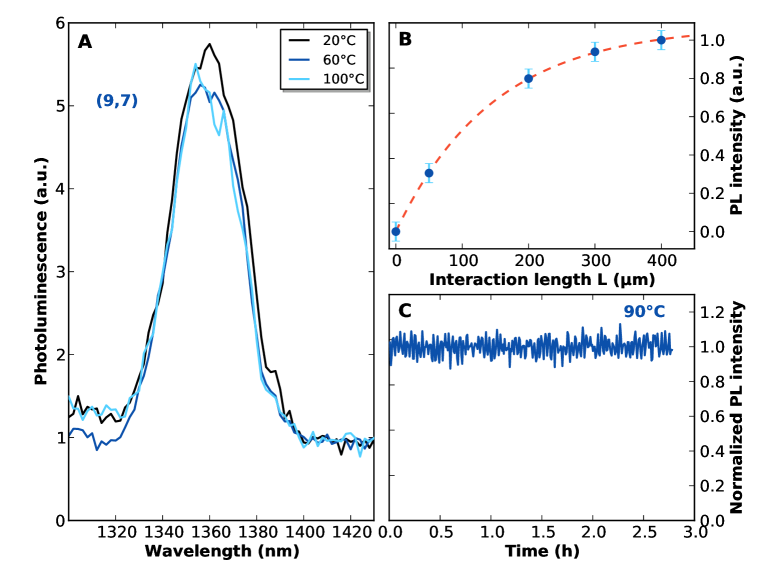
This (9,7) SWNT presents a strong photoluminescence (PL) peak, at a wavelength around 1.35 m, which is identical to the one reported in a thin PFO layer19. The influence of the interaction length on the photoluminescence was also studied for several lengths between 50 m and 400 m. Results are displayed on 4B. For clarity, a point with an interaction length 0 m and PL intensity of 0 was added to results. We noticed that the increase in PL intensity when the interaction length increase is not linear. Indeed, its intensity increase until it reaches a maximum at around 400 m. This evolution could be described by a Beer-Lambert type exponential law, meaning that the observed limitation in photoluminescence intensity is due to the SWNT/PFO layer secondary absorption. These results are consistent with previously obtained results for the absorption coupling and suggest that the optimal interaction length for SWNT/PFO based photonic devices, relying on SWNT absorption or emission properties, would be around 400 m.
In order to furthermore determine the strength of carbon nanotubes for silicon photonic applications, we determined the SWNT emission stability with temperature. That is a major requirement for the achievement of most applications. Evolution of the (9,7) nanotubes emission through the silicon waveguide is presented in 4A for a given interaction length of 400 m. We notice that SWNT PL peak did not shift in wavelength and keep the same intensity level for temperature ranging from 10∘C to 100∘C, which is typically the operating temperature of photonic and microelectronic systems. In order to assess thermal stability over time, PL intensity of (,) SWNT was recorded for 3 hours at 90∘C, and is displayed in 4C. The emission through the waveguide remained constant, and no thermal degradation or intensity decrease was observed.
One important point in the coupling of the photoluminescence of a 1D material such as SWNT into the optical mode of a bulk 3D material like a silicon waveguide, is the coupling efficiency , which is the number of photon effectively transmitted through the waveguide over the total number of photon emitted by carbon nanotubes. That is:
| (2) |
However, this is a very difficult task to undertake in this case. Indeed, is related to SWNT quantum yield , where:
| (3) |
Unfortunately, is not a well-known parameter in carbon nanotubes, and it may vary greatly, in the range to , depending of SWNT diameter, surrounding or length32, 33. In particular, is not yet determined for PFO embedded SWNT.
In any case, it it possible to determine the external effective coupling factor , where:
| (4) |
Knowing the input and output power, the SWNT/PFO thin layer absorbance and the collecting setup transmission, was estimated to be .
If we estimate that carbon nanotubes quantum yield is low (e.g. ), this means that coupling efficiency is of the order of . In the future, the use of photonic cristals or slot waveguides might increase the coupling between carbon nanotubes and silicon waveguides.
In light of the results obtained so far, one could state that carbon nanotubes is a promising material for development of new compact and temperature independent photonics devices on silicon.
2 Conclusions
In conclusion, the integration of carbon nanotubes properties (absorption and photoluminescence) in silicon waveguides was studied using an integration scheme based on evanescent waveguides. The coupling of carbon nanotubes photoluminescence into silicon waveguides has been demonstrated over a wide temperature range. The external effective coupling factor was estimated about . In the future, improved integration schemes based on photonic cristals or slot waveguides will be considered to further increase carbon nanotubes coupling with photonic waveguides in order to fully exploit their extraordinary optical properties to achieve efficient optoelectronic devices in silicon.
3 Materials and Methods
3.1 Carbon nanotubes
Single-wall nanotube powder was purchassed from Unydim Inc. These nanotube were fabricated using the HiPCO process, and were not purified. poly-9,9-di-n-octyl-fluorenyl-2,7-diyl (PFO) was purchassed from Sigma Aldricht. SWNT (5 mg) and PFO (5 mg) were mixed in toluene (30 ml). The mixture was homogeneized, first using a water-bath sonicator for 1h, second, using a tip sonicator at 20 % power for 15 min. In order to remove a part of metallic catalyst particles from the HiPCO process and other impurities, this mixture was then centrifugated using a desktop centrifuge (typically 5-60 min at 10.000 g). The supernatant is then collected and could be drop casted directly onto the photonics devices. The thin film are annealed at 180∘ for 15 min to improve their optical quality.
3.2 Waveguide fabrication
Silicon-on-insulator (SOI) substrate were purchassed from Soitec, with a top silicon layer of 220 nm, and a buried \ceSiO2 layer of 1 m. The technological steps for waveguide fabrication are as follow (see also Supplementary Materials S1):
-
•
Step 1: SOI substrate preparation: Cleaning with acetone under sonication, followed by \ceO2 plasma cleaning.
-
•
Step 2: Waveguides definition into the e-beam resist. Deposition of 300 nm thick MaN negative resist. E-beam patterning at 20 keV, 30 s resist developing in MIF 726.
-
•
Step 3: Pattern transfert: Etching of silicon by RIE down to 6 nm thick silicon layer. RIE: \ceSF6 (20 sccm) and \ceO2 (5 sccm) at 30 W for 70 s.
-
•
Step 4: Waveguide protection by \ceSiO2: 500 nm thick \ceSiO2 layer is deposited on top of silicon waveguides at 300∘C.
-
•
Step 5: Interaction zone definition into the e-beam resist. Deposition of 300 nm thick positive ZEP resist. E-beam patterning at 20 kEV. Developing: 30 s ZED50 / 30 s MIBK / 30 s IPA.
-
•
Step 6: Interaction zone opening: Wet etching with diluted HF of silica down to silicon stopping layer. \ceO2 plasma for resist removal.
-
•
Step 7: SWNT/PFO deposition: 1 m thick SWNT/PFO layer is deposited on the full die followed by a thermal annealing at 180∘C.
-
•
Step 8: SWNT/PFO protection with \ceSiO2: 200 nm thick \ceSiO2 layer is deposited on top of the SWNT/PFO layer at low temperature (150∘C) to prevent layer damage.
-
•
Step 9: Definition of protected zone into the e-beam resist. MaN resist and e-beam patterning, developing.
-
•
Step 10: \ceSiO2 etching using RIE : \ceCHF3 (50 sccm) and \ceO2 (3 sccm) at 325 W (12 mTorr) for 190 s.
-
•
Step 11: Removal of SWNT/PFO outside defined zone by RIE etching. 50 % Ar and 50% \ceO2 at 300 W for 15 min.
3.3 Simulations
Optical simulations were performed using an home-made 2D mode solver based on the full-vectorial finite-difference method34 and focused on anisotropic dielectric waveguides.
The filling factor , measure of the fraction of the mode power flux in the SWNT/PFO layer, is defined by :
where is the SWNT/PFO layer and is the mode power flux.
3.4 Determining
Incoming power density on the silica recess was estimated to be Wm2. A simple assumption is made considering the area around the waveguide whether a nanotube could interact or not. As the profile of the evanescent field is gaussian, it is considered that the whole energy of the optical mode is confined within of the gaussian. That is, a nanotube inside may interact with the waveguide, while a nanotube outside will not interact with the waveguide. Consequently, only the SWNT/PFO thin layer surface inside this limit will be considered. For a waveguide width of 275 nm, the limit is: 360 nm (cf. Supplementary Materials S2). That is, the surface area of the SWNT/PFO layer is = m2. The incident pump power on carbon nanotubes which could couple into the waveguide is W. Absorption of a 1 m thick SWNT/PFO layer at 805 nm is (cf. Supplementary Materials S3). Absorbed power in carbon nanotubes W.
On the other hand, power of the collected photoluminescence from the waveguide was W. The collecting setup losses were estimated to be 2 dB. So the transmitted power was W.
The external effective coupling factor could be determined by:
where is the energy, the frequency and the wavelength of the transmitted and absorbed photons.
Finally, .
Authors would like to thank N. Tang from Univ. Montréal for her proofreading of the manuscript, and D. Marris-Morini and E. Cassan from Univ. Paris Sud for fruitfull discussions.
Detailled technological process of the waveguide fabrication (S1), evanescent mode profile of a 275 nm with waveguide (S2), and absorption spectra of a 1 m thick SWNT/PFO thin layer on silica (S3). This material is available free of charge via the internet at http://pubs.acs.org
References
- Ahmed and Schuegraf 2011 Ahmed, K.; Schuegraf, K. Transistor Wars. IEEE Spectrum 2011, 48, 50–66
- Meindl 2003 Meindl, J. Beyond Moore’s Law: the interconnect era. IEEE Comput. Sci. Eng. 2003, 5, 20–24
- Assefa et al. 2010 Assefa, S.; Xia, F.; Green, W.; Schow, C.; Rylyakov, A.; Vlasov, Y. CMOS-Integrated Optical Receivers for On-Chip Interconnects. IEEE J. Quantum Electron. 2010, 16, 1376–1385
- Zalevsky 2007 Zalevsky, Z. Integrated Micro- and Nanophotonic Dynamic Devices: a Review. J. Nanophoton. 2007, 1, 012504
- Lipson 2005 Lipson, M. Guiding, Modulating, and Emitting Light on Silicon: Challenges and Opportunities. J. Lightw. Tech. 2005, 23, 4222–4238
- Barwicz et al. 2007 Barwicz, T.; Byun, H.; Gan, F.; Holzwarth, C.; Popovic, M.; Rakich, P.; Watts, M.; Ippen, E.; Kärtner, F.; Smith, H. et al., Silicon Photonics for Compact, Energy-Efficient Interconnects. J. Opt. Netw. 2007, 6, 63–73
- Jalali 2008 Jalali, B. Can Silicon Change Photonics? Phys. Stat. Sol. (a) 2008, 205, 213–224
- Liu et al. 2010 Liu, A.; Liao, L.; Chetrit, Y.; Basak, J.; Nguyen, H.; Rubin, D.; Paniccia, M. Wavelength Division Multiplexing Based Photonic Integrated Circuits on Silicon-On-Insulator Platform. IEEE J. Quantum Electron. 2010, 16, 23–32
- Lardenois et al. 2003 Lardenois, S.; Pascal, D.; Vivien, L.; Cassan, E.; Laval, S.; Orobtchouk, R.; Heitzmann, M.; Bouzaida, N.; Mollard, L. Low-Loss Submicrometer Silicon-On-Insulator Rib Waveguides and Corner Mirrors. Opt. Lett. 2003, 28, 1150–1152
- Fang et al. 2007 Fang, A.; Park, H.; Kuo, Y.-H.; Jones, R.; Cohen, O.; Liang, D.; Raday, O.; Sysak, M.; Paniccia, M.; Bowers, J. Hybrid Silicon Evanescent Devices. Mater. Today 2007, 10, 28 – 35
- Ben Bakir et al. 2011 Ben Bakir, B.; Descos, A.; Olivier, N.; Bordel, D.; Grosse, P.; Augendre, E.; Fulbert, L.; Fedeli, J. Electrically Driven Hybrid Si/III-V Fabry-Pérot Lasers Based on Adiabatic Mode Transformers. Opt. Exp. 2011, 19, 10317–10325
- Jurgen et al. 2010 Jurgen, M.; Jifeng, L.; Kimerling, L. High-Performance Ge-On-Si Photodetector. Nature Photon. 2010, 4, 527–534
- Vivien et al. 2009 Vivien, L.; Osmond, J.; Fedeli, J.; Marris-Morini, D.; Crozat, P.; Damlencourt, J.; Cassan, E.; Lecunff, Y.; Laval, S. 42 GHz p.i.n Germanium Photodetector Integrated in a Silicon-On-Insulator Waveguide. Opt. Exp. 2009, 17, 6252–6257
- Reed et al. 2010 Reed, G.; Mashanovich, G.; Gardes, F.; Thomson, D. Silicon Optical Modulators. Nature Photon. 2010, 4, 518–526
- Bachtold et al. 2001 Bachtold, A.; Hadley, P.; T., N.; C., D. Logic Circuits With Carbon Nanotube Transistors. Science 2001, 294, 1317–1320
- O’Connell et al. 2002 O’Connell, M.; Bachilo, S.; Huffmann, C.; Moore, V.; Strano, M.; Haroz, E.; Rialon, K.; Boul, P.; Noon, W.; Kittrell, C. et al., Band Gap Fluorescence from Individual Single-Walled Carbon Nanotubes. Science 2002, 297, 593–596
- Bachilo et al. 2002 Bachilo, S.; Strano, M.; Kittrell, C.; Hauge, R.; Smalley, R.; Weisman, R. Structure-Assigned Optical Spectra of Single-Walled Carbon Nanotubes. Science 2002, 298, 2361–2366
- Nguyen et al. 2011 Nguyen, D.; Roussignol, P.; Roquelet, C.; Lauret, J.; Cassabois, G. Elastic Exciton-Exciton Scattering in Photoexcited Carbon Nanotubes. Phys. Rev. Lett. 2011, 107, 127401
- Gaufrès et al. 2009 Gaufrès, E.; Izard, N.; Vivien, L.; Kazaoui, S.; Marris-Morini, D.; Cassan, E. Enhancement of Semiconducting Single-Wall Carbon-Nanotube Photoluminescence. Opt. Lett. 2009, 34, 3845–3847
- Misewich et al. 2003 Misewich, J.; Martel, R.; Avouris, P.; Tsang, J.; Heinze, S.; Tersoff, J. Electrically Induced Optical Emission from a Carbon Nanotube FET. Science 2003, 300, 783–786
- Marty et al. 2006 Marty, L.; Adam, E.; Albert, L.; Doyon, R.; Ménard, D.; Martel, R. Exciton Formation and Annihilation During 1D Impact Excitation of Carbon Nanotubes. Phys. Rev. Lett. 2006, 96, 136803
- Adam et al. 2008 Adam, E.; Aguirre, C.; Marty, L.; St-Antoine, B.; Meunier, F.; Desjardins, P.; Ménard, D.; Martel, R. Electroluminescence from Single-Wall Carbon Nanotube Network Transistors. Nano Lett. 2008, 8, 2351–2355
- Weisman and Bachilo 2003 Weisman, R.; Bachilo, S. Dependence of Optical Transition Energies on Structure for Single-Walled Carbon Nanotubes in Aqueous Suspension: an Empirical Kataura Plot. Nano Lett. 2003, 3, 1235–1238
- Mueller et al. 2009 Mueller, T.; Kinoshita, M.; Steiner, M.; Perebeinos, V.; Bol, A.; Farmer, D.; Avouris, P. Eficient Narrow-Band Light Emission from a Single Carbon Nanotube p-n Diode. Nature Nanotech. 2009, 5, 27–31
- Gaufrès et al. 2010 Gaufrès, E.; Izard, N.; Le Roux, X.; Marris-Morini, D.; Kazaoui, S.; Cassan, E.; Vivien, L. Optical Gain in Carbon Nanotubes. Appl. Phys. Lett. 2010, 96, 231105
- Kishida et al. 2008 Kishida, H.; Nagasawa, Y.; Imamura, S.; Nakamura, A. Direct Observation of Dark Excitons in Micelle-Wrapped Single-Wall Carbon Nanotubes. Phys. Rev. Lett. 2008, 100, 097401
- Izard et al. 2011 Izard, N.; Gaufrès, E.; Le Roux, X.; Kazaoui, S.; Murakami, Y.; Marris-Morini, D.; Cassan, E.; Maruyama, S.; Vivien, L. Electroabsorption Study of Index-Defined Semiconducting Carbon Nanotubes. Eur. Phys. J. Appl. Phys. 2011, 55, 20401
- Freitag et al. 2003 Freitag, M.; Martin, Y.; Misewich, J.; Martel, R.; Avouris, P. Photoconductivity of Single Carbon Nanotubes. Nano Lett. 2003, 3, 1067–1071
- St-Antoine et al. 2011 St-Antoine, B.; Ménard, D.; Martel, R. Single-Walled Carbon Nanotube Thermopile for Broadband Light Detection. Nano Lett. 2011, 11, 609–613
- 30 International Technology Roadmap for Semiconductors, 2009 ed., \urlhttp://www.itrs.net
- Gaufrès et al. 2010 Gaufrès, E.; Izard, N.; Le Roux, X.; Kazaoui, S.; Marris-Morini, D.; Cassan, E.; Vivien, L. Optical Microcavity With Semiconducting Single-Wall Carbon Nanotubes. Opt. Exp. 2010, 18, 5740–5745
- Berciaud et al. 2008 Berciaud, S.; Cognet, L.; Lounis, B. Luminescence Decay and the Absorption Cross Section of Individual Single-Walled Carbon Nanotubes. Phys. Rev. Lett. 2008, 101, 077402
- Hertel et al. 2010 Hertel, T.; Himmelein, S.; Ackermann, T.; Stich, D.; Crochet, J. Diffusion Limited Photoluminescence Quantum Yields in 1-D Semiconductors: Single-Wall Carbon Nanotubes. ACS Nano 2010, 4, 7161–7168
- Fallahkhair et al. 2008 Fallahkhair, A.; Li, K.; Murphy, T. Vector Finite Difference Modesolver for Anisotropic Dielectric Waveguides. J. Lightw. Technol. 2008, 26, 1423–1431