Surface plasmon polaritons scattering by subwavelength silicon wires
Abstract
Surface plasmon polaritons scattering from 2D subwavelength silicon wires is investigated using finite difference time domain method. It is shown that coupling an incident surface plasmon polariton to inter-cavity modes of the particle can dramatically changes transmitted fields and plasmon-induced forces. In particular, both transmission and optical forces are highly sensitive to the particle size that is related to the excitation of whispering gallery modes or standing-wave modes depending on the particle shape and size. This features might have potential sensing applications.
I Introduction
Surface plasmon polaritons (SPP’s) are evanescently confined modes that propagate at the interface between a dielectric and a conductor. This confinement leads to an enhancement of electromagnetic fields at the interface which is very sensitive to the surface defects Polanco et al. (2013); Brucoli and Martín-Moreno (2011). The unique properties of the SPPs give them two dimensional nature and opens an opportunity for scaling down optical devices to nanometric dimensions Maier (2007); Gramotnev and Bozhevolnyi (2010). In order to understand basic behaviors of such devices the interaction of SPPs with small particles and defects is a problem of fundamental importance. While, scattering by surface defects in all-metal structures has been studied in many works Polanco et al. (2013); Brucoli and Martín-Moreno (2011); Pincemin et al. (1994); Nikitin et al. (2007), scattering by dielectric objects placed near a metallic surface has been explored less so far. The study of the latter structure might be particularly useful in the plasmonic optical tweezers in which a small object is trapped near a metallic surface Min et al. (2013); Zhang et al. (2014); Wang et al. (2009); Righini et al. (2008). SPP scattering by finite-size gold nanocubes placed in the vicinity of a metal surface has been analyzed in Ref. Evlyukhin et al. (2007), and scattering by 2D rectangular dielectric particles has also been analyzed Pincemin et al. (1994).
While silicon is widely used in conventional photonic devices, it also provides an important material for the design of silicon plasmonic devices with advanced functionalities. Resonant light interactions of high-refractive index dielectric nanoparticles have already been analyzed in details Evlyukhin et al. (2014); Van de Groep and Polman (2013). Here, we consider their interactions with surface plasmon polaritons. It is well-known from Mie theory that for dielectric particles with higher refractive indexes, the light scattering efficiency increases. Due to these properties, high index dielectric material offer great practical advantages in many plasmonic structures such as low loss propagation and strong field confinement in the hybrid plasmonic waveguides Oulton et al. (2008); Yang et al. (2011); Chen et al. (2012) and enhanced light transmission and enhanced trapping forces in the plasmonic nanoaperture traps Garcia de Abajo (2002); Aporvari et al. (2015).
Dielectric microcavities can support whispering gallery modes (WGMs) which have been intensively applied to many devices such as optical sensors He et al. (2011), narrowband filters Savchenkov et al. (2009), and microlasers Polman et al. (2004). Most research on WGM cavities are restricted to large cavities with sizes much larger than light wavelength. However, to develop advance nanophotonic elements, it is of great importance to consider nanosize resonators with sizes smaller than the considered light wavelength. In this regime there are few research on WGMs (see, for instance Nobis et al. (2004); Cole et al. (2006)). In this paper we consider subwavelength silicon wires and investigate the excitation of WGMs with small mode numbers.
From the theoretical perspective, the scattering of surface plasmon polaritons by surface defects has been studied by several techniques such as the Green’s Function method Paulus and Martin (2001); Pincemin et al. (1994) and Rayleigh expansion method Nikitin et al. (2007); Polanco et al. (2013); Zayats et al. (2005). On the other hand, the finite difference time domain (FDTD) method is a powerful and well known technique to determine electromagnetic fields around nanostructures of complex and arbitrary geometries Taflove and Hagness (2005); Oubre and Nordlander (2005); Kuttge et al. (2009); Okamoto and Kawata (1999). In this paper, we use two-dimensional FDTD method (a home-made code) for analyzing SPPs scattering from subwavelength silicon wires with different cross sections. We also use the Maxwell stress tensor (MST) technique to investigate the optical forces on the particles. We show that SPP scattering parameters and optical forces on a subwavelength wire are non-trivial and strongly depend on its cross section shape and size. Indeed, our calculations show that the excitation of intercavity modes such as WGMs and standing wave modes, is responsible for this behavior. It is important to note that the high refractive index plays a key role here and for sufficiently high refractive index material such as silicon, the subwavelength wire would exhibit WGMs (with small mode numbers) even if its size is smaller than the vacuum wavelength of the light. Although they are less investigated, such low order modes in subwavelength regime could be of great importance for nanophotonics and nanosized devices Nobis et al. (2004).
II Calculation of Optical Forces
To excite SPPs in the FDTD simulations we use the total-field/scatter-field technique (Taflove and Hagness, 2005). A small grid size (less than ) is chosen in order to account for all plasmonic near-field behaviors. We bound the simulation domain with a convolutional perfectly matched layer (CPML) Taflove and Hagness (2005). For the dielectric constant of the metallic region, we use the Drude model with parameters that fitted to the experimental data of the complex dielectric constant for silver Johnson and Christy (1972).
Once the electromagnetic fields have been calculated using FDTD method, we can calculate the optical forces acting on the particle using the Maxwell stress tensor (MST) method Novotny and Hecht (2012). The time-averaged force acting on the center of mass of the particle is
| (1) |
where is a surface enclosing the particle, is the unit vector perpendicular to the surface, and is the time-averaged Maxwell stress tensor for harmonic fields, i.e.,
| (2) |
where E is the electric field, H is the magnetic field, and and are the permittivity and permeability of the surrounding medium.
We notice that for small particles or small entities in the structure (like small gaps) and for low refractive index discrepancy between dielectric particle and surrounding, the force calculations using the Maxwell stress tensor need a lot of care. In order to ensure the correctness of our results we verified the numerical convergence of our algorithms. In our simulations we considered a uniform two-dimensional square-cell space lattice with . For each configuration we performed a convergence analysis to ensure that the mesh size is chosen properly (i.e. it is small enough) to reduce numerical errors. As a result of this analysis we decided to employ a mesh size between 2 nm and 3 nm.
III Comparison of FDTD Computations and Rayleigh Expansion Approximation
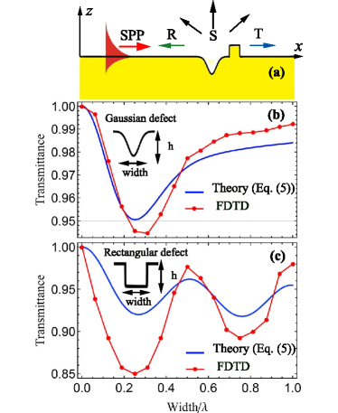
It is instructive to first compare FDTD computations with a theoretical model. We consider the scattering of SPPs by small defects on a metal-vacuum interface. As shown in Fig. 1 a SPP of frequency propagates along the x axis. Suppose that the metal-vacuum interface is describe by the following function:
| (3) |
This form represents a one-dimensional defect in a single interface all-metal structure. For small defects, the magnetic field in the vacuum half-space can be written as a sum of the incident field and scattered field according to the conventional Rayleigh expansion Tsang et al. (2004):
| (4) |
where , are the wave number of a surface plasmon polariton at a flat metal-vacuum interface and the inverse decay length of the fields perpendicular to the interface, respectively. Also, is the dielectric function of the metallic half space, , and is defined by , Re.
In order to find scattered coefficients, , assuming that , one can apply the surface impedance boundary condition (SIBC) to the tangential components of the fields at metal surface Nikitin et al. (2007). As a result, the reflected and transmitted SPP fields may be written in the following form
| (5) | |||
| (6) |
where and are parameters to be calculated using the boundary conditions Nikitin et al. (2007). Therefore, the transmission and reflection coefficients are
| (7) |
Also, the energy conservation law leads to scattering coefficient from .
Figure 1 illustrates the results for two defect of rectangular (b) and Gaussian (c) profiles in a silver surface (at a wavelength of 600 nm). We also perform two-dimensional FDTD method to compare the results. As seen in the figure, there is a noticeable discrepancy between the FDTD results and the theoretical prediction of Rayleigh approximation. This discrepancy might be attributed to the simplified boundary conditions and ignoring the propagation losses in (5). Furthermore, here the defect depths , , is relatively large. Note that, for rectangular defect there is much less agreement which could be attributed to the violation of the surface impedance boundary condition at the discontinuity points. However, for smooth and sufficiently shallow defects one would expect the Rayleigh approximation leads to more accurate results Nikitin et al. (2007).
IV Scattering by subwavelength particles
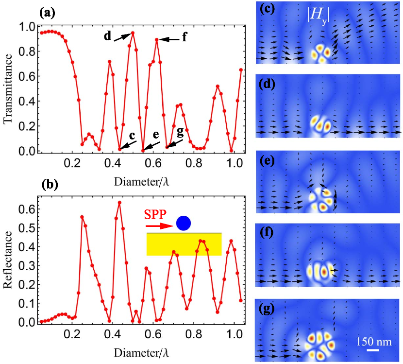
Let us now apply FDTD method to study the scattering of surface plasmon polaritons by subwavelength silicon wires. We first consider scattering of a SPP from a circular silicon cylinder placed near a flat silver surface. The surrounding medium in the half-space is water (refractive index ), and the refractive index of Si was taken from Ref. Palik (1998). We fixed the gap between the particles and metal surface as 12 nm. Figs. 2 (a) and (b) show transmittance and reflectance as a function of the particle diameter. As can be seen the particle behave in two different ways depending to its diameter. First, for very small particles () most incident SPP is transmitted, however larger particles transmit less power. Second, for larger particles () the transmittance and reflectance curves strongly fluctuates. In this case, the transmittance suddenly rises and falls and surprisingly, in some points it is very high and in some points it is approximately zero. To better understand these behaviors, the magnetic field distribution () and Poynting vector field are shown in Figs. 2 (c)-(g) for some particle of interest (depicted in Fig. 2 (a) with arrows). For instance, Fig. 2 (c) shows excitation of second-order (azimuthal) transverse magnetic (TM) polarized Whispering Gallery mode (WGM) by evanescent coupling of incident SPP (here, the radius of the wire is 130 nm, which corresponds to Diameter/wavelength=0.433). More precisely, the whispering gallery modes, , of a 2D cylindrical cavity of radius can be analytically found by solving Helmholtz equation using the separation variable technique Foreman et al. (2015). The solutions take the form,
| (8) |
where the function is Bessel function of first kind, , for and the Hankel function of the first kind, , for . Each mode is labeled as two mode numbers (N, m) which are the radial and azimuthal mode numbers. The mode numbers N and m are also related to the number of maxima in the field profile in the radial and azimuthal direction, respectively. Therefore, the field profile in Fig. 2 (c) corresponds to the mode (1, 2). From field intensity and Poynting vector distribution, we can conclude that the excitation of resonant particle modes lead to a negligible SPP transmission. In this case, the coupling of incident SPP to the WGMs of the particle is very similar to the critical coupling in the microcavity-waveguide systems, in which the directly transmitted field and the field coupled out of resonator into the output waveguide are out of phase and thus vanish each other Vahala (2004). We remark that, similar plasmonic transmission behavior has been reported in the SPPs scattering by deep narrow grooves structured into flat gold surfaces Kuttge et al. (2009), for which efficient coupling of incident SPPs to resonant cavity modes inside the grooves leads to high reflectivity. It is also clear from Poynting vector pattern in Fig. 2 (c) that most incident power scatters to the radiation fields into the forward direction.
In a simple geometric optics picture, modes of order m correspond to a plane wave with propagation constant of , undergo multiple total internal reflection upon the interior surface of the resonator. After one full circulation within the cavity ( in (8)) we can write:
| (9) |
where , is the feedback path and is the polarization-dependent phase shift that occurs during each total internal reflection Jackson and Jackson (1962). Note that, the ray optics approximation is more suitable for large cavities, i. e. , however it can also describe low-order WGMs Nobis et al. (2004). For a fixed wavelength we see from (9) that which show that higher mode number needs longer paths and therefore larger cavities. In fact, it is possible to excite higher order WGMs with increasing the particle diameter as demonstrated in Figs. 2 (e) and (g) (for (N,m)=(1, 3) and (1, 4)). The Poynting vector field also demonstrate how the field scattered in different directions for different particles. Figures 2 (d) and (f) illustrate the field patterns for nonresonant configurations where as can be seen most input power conveys to the transmitted surface plasmon polariton. So, the coupling of SPP mode to inter cavity modes of the particle leads dramatically changes in the transmission, reflection and scattering coefficients. This sensitivity of the transmitted SPPs to the particle size might be useful for single particle sensing down to subwavelength scales. In fact, the penetration of the evanescent near-field to the upper dielectric medium makes the SPPs sensitive to the refractive index changes in their local environment. The presence of the particle can be easily determined because coupling between the SPP and particle causes a strong transmission change. Here, all-optical excitation and detection is one of the most important advantages of SPP sensing.
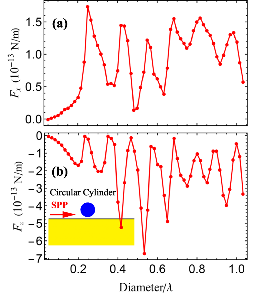
We now investigate the optical force on the particles near a metal surface. Large field enhancement near a metallic surface allows efficient optical trapping using evanescent plasmonic fields. Conventional optical traps have been widely used for manipulation of small dielectric particles and living cells, although the size of trapped objects are usually larger than the light wavelength. Plasmonic optical traps make it possible to effectively trap smaller subwavelength particles on a flat surface at low input power Aporvari et al. (2015). Also, the surface plasmon radiation pressure can be used for particle transport in a liquid environment Wang et al. (2013). Here, we show how the particle sizes strongly affect the scattering and gradient plasmonic forces.
The normal and lateral optical forces has been demonstrated in Fig. 3. Again, we have two separate regains: small particle region where both and magnitudes are increased with increasing particle size and fluctuating force region. However, for very small particles, due to strong field gradient of the SPP wave perpendicular to the surface the attractive normal force, is much larger than scattered lateral force, . In the fluctuating region we see the excitation of WG modes strongly affects the force magnitudes. We should note that similar behavior was reported from an incident plane wave on spherical dielectric particles Jia and Thomas (2009). However, for SPP incident wave the force fluctuations are much stronger compared to the plane wave incident.
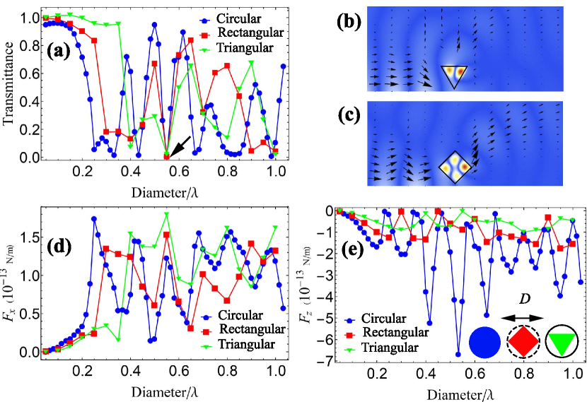
Next, we shortly explore the influence of particle shape to the transmittance and optical forces. The results are shown in Fig. 4. For comparison we again show the circular particle transmittance and forces. The size of square and equilateral triangle particle are define as the diameter of the circle circumscribing the particle. As can be seen, the particle shape has considerable influence on the transmittance. However, notice that, for some particle sizes (see, e.g., the arrow in Fig. 4 (a)), all three particles show a resonant behavior, but the excited modes are different. Their magnetic field patterns are illustrated in Fig. 2 (e) and Figs.4 (b)-(c). It is possible to excite a standing wave mode for square particles. In fact, careful monitoring of the instantaneous magnetic field over one period reveals that the mode profile of the particle of Fig. 4 (c) is a standing wave mode. The standing wave pattern can be given as , where and are coordinates in the directions of the square sides of length a. We can thus deduce that Fig. 4 (c) shows the excitation of the mode .
The induced optical forces are plotted in Figs. 4 (d)-(e) which again show high shape dependence. Particularly, is much bigger for circular particles compared to the square and triangular particles.
V conclusions
In conclusion, surface plasmons scattering by subwavelength defects and particles has been investigated using two dimensional finite difference time domain method. It is shown that even for small subwavelength particles the excitation of WG modes or standing wave modes strongly affects the transmittance and reflectance of SPPs, which might have potential sensing applications. It is also shown that this mode excitation strongly influences the optical forces acting on the particle. While in this work we consider the 2D scattering problem, it can be straightforwardly extended to more general structures, e.g., SPPs scattering by nanorods at oblique incidence.
References
- Polanco et al. (2013) J. Polanco, R. Fitzgerald, and A. Maradudin, Physical Review B 87, 155417 (2013).
- Brucoli and Martín-Moreno (2011) G. Brucoli and L. Martín-Moreno, Physical Review B 83, 045422 (2011).
- Maier (2007) S. A. Maier, Plasmonics: fundamentals and applications (Springer Science & Business Media, 2007).
- Gramotnev and Bozhevolnyi (2010) D. K. Gramotnev and S. I. Bozhevolnyi, Nature photonics 4, 83 (2010).
- Pincemin et al. (1994) F. Pincemin, A. Maradudin, A. Boardman, and J.-J. Greffet, Physical Review B 50, 15261 (1994).
- Nikitin et al. (2007) A. Y. Nikitin, F. López-Tejeira, and L. Martin-Moreno, Physical Review B 75, 035129 (2007).
- Min et al. (2013) C. Min, Z. Shen, J. Shen, Y. Zhang, H. Fang, G. Yuan, L. Du, S. Zhu, T. Lei, and X. Yuan, Nature communications 4 (2013).
- Zhang et al. (2014) Y. Zhang, J. Wang, J. Shen, Z. Man, W. Shi, C. Min, G. Yuan, S. Zhu, H. P. Urbach, and X. Yuan, Nano Lett. 14, 6430 (2014).
- Wang et al. (2009) K. Wang, E. Schonbrun, and K. B. Crozier, Nano letters 9, 2623 (2009).
- Righini et al. (2008) M. Righini, C. Girard, and R. Quidant, Journal of Optics A: Pure and Applied Optics 10, 093001 (2008).
- Evlyukhin et al. (2007) A. Evlyukhin, G. Brucoli, L. Martín-Moreno, S. Bozhevolnyi, and F. García-Vidal, Physical Review B 76, 075426 (2007).
- Evlyukhin et al. (2014) A. B. Evlyukhin, R. L. Eriksen, W. Cheng, J. Beermann, C. Reinhardt, A. Petrov, S. Prorok, M. Eich, B. N. Chichkov, and S. I. Bozhevolnyi, Scientific reports 4 (2014).
- Van de Groep and Polman (2013) J. Van de Groep and A. Polman, Optics express 21, 26285 (2013).
- Oulton et al. (2008) R. F. Oulton, V. J. Sorger, D. Genov, D. Pile, and X. Zhang, Nature Photonics 2, 496 (2008).
- Yang et al. (2011) X. Yang, Y. Liu, R. F. Oulton, X. Yin, and X. Zhang, nano Letters 11, 321 (2011).
- Chen et al. (2012) L. Chen, T. Zhang, X. Li, and W. Huang, Optics express 20, 20535 (2012).
- Garcia de Abajo (2002) F. Garcia de Abajo, Opt. Express 10, 1475 (2002).
- Aporvari et al. (2015) M. S. Aporvari, F. Kheirandish, and G. Volpe, Optics Letters 40, 4807 (2015).
- He et al. (2011) L. He, Ş. K. Özdemir, J. Zhu, W. Kim, and L. Yang, Nature nanotechnology 6, 428 (2011).
- Savchenkov et al. (2009) A. Savchenkov, W. Liang, A. Matsko, V. Ilchenko, D. Seidel, and L. Maleki, Optics letters 34, 1318 (2009).
- Polman et al. (2004) A. Polman, B. Min, J. Kalkman, T. Kippenberg, and K. Vahala, Applied Physics Letters 84, 1037 (2004).
- Nobis et al. (2004) T. Nobis, E. M. Kaidashev, A. Rahm, M. Lorenz, and M. Grundmann, Physical review letters 93, 103903 (2004).
- Cole et al. (2006) R. Cole, Y. Sugawara, J. Baumberg, S. Mahajan, M. Abdelsalam, and P. Bartlett, Physical review letters 97, 137401 (2006).
- Paulus and Martin (2001) M. Paulus and O. J. Martin, JOSA A 18, 854 (2001).
- Zayats et al. (2005) A. V. Zayats, I. I. Smolyaninov, and A. A. Maradudin, Physics reports 408, 131 (2005).
- Taflove and Hagness (2005) A. Taflove and S. C. Hagness, Computational electrodynamics (Artech House, 2005).
- Oubre and Nordlander (2005) C. Oubre and P. Nordlander, The Journal of Physical Chemistry B 109, 10042 (2005).
- Kuttge et al. (2009) M. Kuttge, F. J. García de Abajo, and A. Polman, Optics express 17, 10385 (2009).
- Okamoto and Kawata (1999) K. Okamoto and S. Kawata, Physical review letters 83, 4534 (1999).
- Johnson and Christy (1972) P. B. Johnson and R.-W. Christy, Phys. Rev. B 6, 4370 (1972).
- Novotny and Hecht (2012) L. Novotny and B. Hecht, Principles of nano-optics (Cambridge university press, 2012).
- Tsang et al. (2004) L. Tsang, J. A. Kong, and K.-H. Ding, Scattering of Electromagnetic Waves, Theories and Applications, Vol. 27 (John Wiley & Sons, 2004).
- Palik (1998) E. D. Palik, Handbook of optical constants of solids, Vol. 3 (Academic press, 1998).
- Foreman et al. (2015) M. R. Foreman, J. D. Swaim, and F. Vollmer, Advances in Optics and Photonics 7, 168 (2015).
- Vahala (2004) K. Vahala, Optical microcavities (World Scientific, 2004).
- Jackson and Jackson (1962) J. D. Jackson and J. D. Jackson, Classical electrodynamics, Vol. 3 (Wiley New York etc., 1962).
- Wang et al. (2013) X. Wang, K. Xiao, C. Min, Q. Zou, Y. Hua, and X.-C. Yuan, Plasmonics 8, 637 (2013).
- Jia and Thomas (2009) L. Jia and E. L. Thomas, JOSA B 26, 1882 (2009).