Terahertz pulsed photogenerated current in microdiodes at room temperature
Abstract
Space-charge modulation of the current in a vacuum diode under photoemission leads to the formation of beamlets with time periodicity corresponding to THz frequencies. We investigate the effect of the emitter temperature and internal space-charge forces on the formation and persistence of the beamlets. We find that temperature effects are most important for beam degradation at low values of the applied electric field, whereas at higher fields intra-beamlet space-charge forces are dominant. The current modulation is most robust when there is only one beamlet present in the diode gap at a time, corresponding to a macroscopic version of the Coulomb blockade. It is shown that a vacuum microdiode can operate quite well as a tunable THz oscillator at room temperature with an applied electric field above 10 MV/m and a diode gap of the order of 100 nanometers.
pacs:
52.59.Rz, 73.23.Hk, 29.20.Introduction. Space-charge limited flow in a diode has been a subject of investigation for over a century Child (1911); Langmuir (1913); Birdsall (1966). Nonetheless, this field of research remains quite fertile in terms of interesting results. The past fifteen years have seen considerable work on extending the classical Child-Langmuir law Luginsland et al. (2002), e.g. for very small structures Ang et al. (2006, 2003); Zhu and Ang (2011), finite emitter area and pulse length Valfells et al. (2002a); Lau (2001); Ang and Zhang (2007), space-charge limited field emission Feng and Verboncoeur (2006); Rokhlenko et al. (2010); Torfason et al. (2015), as well as development of novel scaling laws and investigations into the nature of space-charge limited flow Akimov et al. (2001); Caflisch and Rosin (2012); Griswold et al. (2010); Zhu et al. (2013).
Recent research has been on the formation of regular electron bunches under space-charge limited conditions in microdiodes Pedersen et al. (2010). Simulations and analysis indicate that in diodes with gap spacing from hundreds of nm to a couple of microns, and applied potential of the order of Volts, space-charge effects can lead to the formation of well defined electron bunches at the cathode, that lead to a regularly varying anode current, Fig. 1. The frequency of this current is in the THz band and can be tuned by simply varying the applied electric field inside the diode Jonsson et al. (2013). Furthermore, it appears that higher power can be extracted from the diode if the cathode is covered with an array of nanoscale emitting „dots“ each emitting a stream of beamlets that is synchronized with the beamlets from neighboring emitters Ilkov et al. (2015). A recent paper that presents a study on the maximal charge allowed for stable injection of electron bunches into a diode with a regular interval Liu et al. (2015b) has some interesting parallels to our previous work, although the geometry and operating parameters are not directly comparable.
Although this is an interesting idea for THz generation and applications Siegel et al. (2002); Booske et al. (2011); Jepsen et al. (2011); Tonouchi (2007), there is still a fundamental issue that needs to be addressed. Under what circumstances can one expect to still see the time dependent structure intact? Two particular candidate causes for degradation of the beamlets are: velocity spread (or emittance); and Coulomb forces causing beamlets to expand and merge. In this paper we will investigate the issue by looking in detail at how diode gap spacing, applied potential and velocity spread of electrons emitted from the cathode influence pulse formation and degradation.
Physical and simulation setup. The system under study is an infinite parallel plate vacuum diode, with gap spacing , sketched in Fig. 1. Emission from the cathode is restricted to a circular area of radius R = 150 nm. A voltage is applied across the diode gap, , and it is kept constant throughout one simulation. The vacuum field for a diode without any electrons in the gap is .
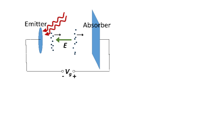
Emission is not source limited, so we assume unlimited supply of electrons. This creates in turn, space-charge limited current in the diode gap. The flow of current is as follows: Once the device is turned on, a bunch starts to form in front of the emitter. To extract an electron from a particular emitter location, the surface field must point towards the emitter, i.e. that spot must be favorable for emission. If so, emission is permitted and the emitted electron can probably be accelerated towards the absorber. We say probably because, the electrons already in the gap may position themselves in such a way that, later on, they can push this electron back into the emitter. After this, a new, random spot is checked on the cathode. If the new spot is favorable, as before, an electron is placed 1 nm above the surface of the cathode. This is done to ensure that the normal component of the electric field on the cathode due to the newly placed electron is nonzero. In reality such emitters will have surface irregularities which will be larger than 1 nm which permits us to choose such distance for electron placement. The numerical results are not sensitive to the exact height of placement as long as it is much smaller than the gap spacing Jonsson et al. (2013). If an unfavorable spot is found, a new one is randomly picked and tested. If in hundred consecutive checks, no favorable spot is found, the cathode is deemed unfavorable for emission and the code continues to the next step which is the advancement of the electrons.
Now, the forces between all electrons in the diode gap are calculated together with the forces due to the applied vacuum field. These forces, coupled with the basic Verlet method Grubmüller et al. (1991); Hairer et al. (2003); Marx and Hutter (2009), advance the electrons for the duration of one time step, s. After that, it is checked whether electrons have entered the anode, or if due to Coulomb forces they are pushed back into the cathode by the electrons ahead. If they did, the time and place of absorption is noted and the electrons are taken out of the system. In this moment one time step is finished, and a new time step begins with the emission process all over again. The complete explanation and setup of the system is given in detail in previous work, but only for initial velocities of electrons equal to zero Jonsson et al. (2013); Pedersen et al. (2010). In this present paper we consider non-zero initial velocities.
For the photoemission process Jensen and Montgomery (2009); Jensen et al. (2007) we will divide the emission region into two separate regions: metal and vacuum. The energy of electrons inside the metal corresponds to the free electron gas and it is governed by the Fermi-Dirac statistics. The energy of the vacuum state is , where is the Fermi energy and
| (1) |
is the work function, is the Schottky work function, and is the height of the photoemission potential barrier. The energy after emission is equal to . If the laser used for photoemission can be tuned such that , then the electron energy will be distributed by the Maxwell-Boltzmann statistics Dowell and Schmerge (2009); Neppl (2012); Jensen et al. (2010, 2012, 2014). The fact that the Fermi-Dirac distribution is virtually identical to the Maxwell-Boltzmann distribution for energies higher than at room temperature justifies using Maxwell-Boltzmann for the electron density of states Jensen et al. (2010). A mismatch between the laser energy and the work function is allowable as long as it is much smaller that the thermal energy , being the Boltzmann constant and the temperature. Also, the electrons available for emission come only from the highest energy states. The aim of this paper is to try to model a room temperature device, therefore the interest is in the high temperature tail of the distributions. We consider the Maxwell-Boltzmann distribution of electron velocities at the emitter surface, in the spatial direction ,
| (2) |
being the mass of the electron. The velocities in the propagation direction , i. e. from left to right in Fig. 1, can only have positive values, whereas those in the perpendicular directions and can take any value.
Results and analysis. We will now show the results in parameter space. The temperatures tested are K. They are shown on the horizontal axes in the following figures. The gap spacing, i.e. the distance between emitter and absorber, has values nm, shown on the vertical axes. Each figure is made with a fixed value of the electric field, MV/m.
For each combination of parameters we run six simulations. The total simulated time for each case was s. For the systems with lowest frequencies ( THz) we get 300 bunching events and for the highest frequencies ( THz) about 800 bunching events in total.
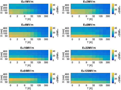
Averaged signal-to-noise ratio (SNR). The averaged SNR is a good measure of the quality of the beam modulation. It is calculated using the peak amplitude of the Fourier spectrum of the diode current and the average amplitude of the noise , as . The computational algorithm uses unfiltered Fourier transform and searches for the highest peak in a predetermined region. This region can be found through the parameterization given in Jonsson et al. (2013) where is the frequency measured in Hz (with the applied vacuum field in units of V/m). The parameters and depend on the size of the emitter, i.e. the radius of the disk. Table 1 shows values of these parameters for three emitter radii.
| Emitter radius [nm] | A | |||
|---|---|---|---|---|
| 50 | 0.539 | |||
| 100 | 0.580 | |||
| 250 | 0.575 |
If the spectrum contains higher harmonics, as it often does, the algorithm chooses only the first harmonic for the analysis. Although higher harmonics can carry a significant portion of the energy, keeping with the conservative nature of this research, only the first, and always highest, peak is chosen.
From Fig. 2 it can be seen that the transition from the parameter space where the SNR is high to that where it is low is more dependent on temperature (an almost vertical boundary) for low values of the applied field and becomes more dependant on the gap spacing (an almost horizontal boundary) as field strength increases. The reason for this is that the number of electrons per bunch increases with applied electric field, which leads to greater intra-beam space-charge forces, which in turn come to dominate thermal effects as the cause of degradation. Although the definition of what constitutes a good signal-to-noise ratio is somewhat arbitrary and application dependant, we consider the SNR to be good if it is above 20 dB.
We notice that the highest SNR for MV/m occurs at nm instead of 50 nm as for other fields. This is because the degradation of the beamlets is a complex process. A long transit time allows beamlets to spread, but so does a greater number of electrons per bunch. However, since such an effect is not apparent at room temperature a detailed investigation is beyond the purpose of the present work.
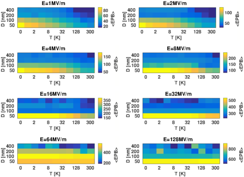
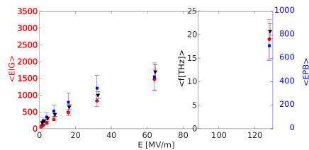
Average number of electrons per bunch (EPB). The number of EPB increases with increasing electric field due to the fact that more electrons per bunch are needed to create field reversal at the emitter surface Pedersen et al. (2010). The total number of electrons in the gap is proportional to the applied field (see Eq. (4) of Valfells et al. (2002a) and Eq. (7) of Jonsson et al. (2013)). For a constant field the total number of electrons is nearly constant, but a larger gap can accomodate more bunches, leading to fewer EPB. The number of EPB also increases with decreasing the temperature, since the bunches have more definitive structure and less smearing, Fig. 3. This creates robust and solid bunches which block the cathode for a long time before another bunch is formed. As the temperature is increased bunch destruction begins much faster after formation. Because no real blockade on the cathode is created another bunch forms much sooner than it would happen at lower temperatures. This might mean more bunches in the gap with increasing temperature, as can be seen in Fig. 4, but each bunch has fewer electrons and the current begins to resemble a continuous stream.
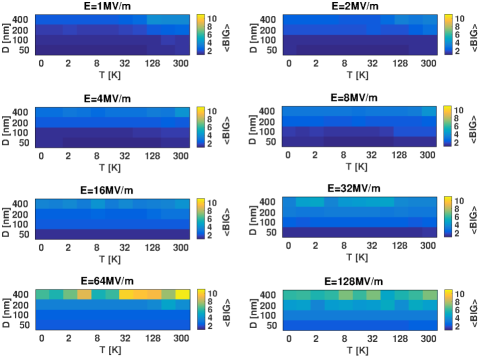
Average number of bunches in the gap (BIG). The number of BIG increases with increasing vacuum field, gap spacing, and more subtly with temperature. As the vacuum field increases, the total number of electrons in the gap also grows and this means more bunches in the gap. This comes from the simple Child-Langmuir law Langmuir (1913). Similarly, increasing gap spacing means more space and more bunches can be accommodated into it. As the temperature increases, the initial velocity of the electrons increases as well. This lowers the blocking potential from the charge already present in the gap, the emission is facilitated, and the virtual cathode from the electrons already present in the gap can be more easily overcome. If the temperature is low, all electrons exit the emitter with similar velocities and the bunch is more narrow in the direction of propagation. The (average number per bunch) shows that the signal quality decreases with increasing this number. Which means that THz signal is the strongest at .
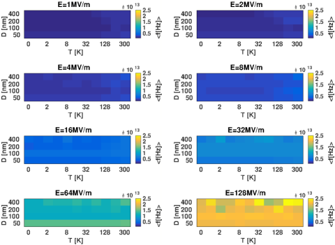
Frequency. It has been shown Jonsson et al. (2013) that the current frequency depends only on the electric field for zero emission velocity. That is why all the plots of Fig. 5 show roughly homogeneous color; the frequency doesn’t change with changing temperature, nor gap spacing. Apparent variations in peak frequency with increased temperature and gap spacing are numerical artefacts due to the fact that in the parameter regions where the bunches are poorly defined, the exact value of the peak frequency is hard to define. The average number of electrons in the diode gap (EIG) obtained for all temperatures and gap spacings, but at a fixed electric field, is shown in Fig. 6. This number increases simply due to the increasing space-charge limited current density given by the classical Child-Langmuir law Langmuir (1913). On the same figure we can see the average EPB. This was done as a way to cross check our work with previous work Valfells et al. (2002a).
Conclusion. THz radiation with microdiodes where several bunches are present in the gap can be maintained only at temperatures below 10 K. Although such temperatures are attainable they are impractical for real world operation. In this paper we showed that if the number of bunches in the system can be controlled to be close to one, the SNR significantly improves. Such systems can have a high SNR ( dB) even at room temperature.
This work was funded by the Icelandic Research Fund grant 120009021. AM acknowledges additional support from COST Action MP1204. We are thankful to Samuel Perkin from Reykjavik University and Kevin Jensen from the US Naval Research Laboratory for useful comments.
References
- Child (1911) C. Child, Phys. Rev. (Series I) 32, 492 (1911).
- Langmuir (1913) I. Langmuir, Phys. Rev. 2, 450 (1913).
- Birdsall (1966) C. K. Birdsall and W. B. Bridges, Electron dynamics of diode regions (New York: Academic Press, 1966).
- Luginsland et al. (2002) J. Luginsland, Y. Lau, R. Umstattd, and J. Watrous, Physics of Plasmas 9, 2371 (2002).
- Ang et al. (2006) L. K. Ang, W. Koh, Y. Lau, and T. Kwan, Physics of Plasmas 13, 056701 (2006).
- Ang et al. (2003) L. Ang, T. Kwan, and Y. Lau, Phys. Rev. Lett. 91, 208303 (2003).
- Zhu and Ang (2011) Y. Zhu and L. Ang, Appl. Phys. Lett. 98, 051502 (2011).
- Valfells et al. (2002a) A. Valfells, D. Feldman, M. Virgo, P. O’shea, and Y. Lau, Physics of Plasmas 9, 2377 (2002a).
- Lau (2001) Y. Lau, Phys. Rev. Lett. 87, 278301 (2001).
- Ang and Zhang (2007) L. Ang and P. Zhang, Phys. Rev. Lett. 98, 164802 (2007).
- Feng and Verboncoeur (2006) Y. Feng and J. Verboncoeur, Physics of Plasmas 13, 073105 (2006).
- Rokhlenko et al. (2010) A. Rokhlenko, K. L. Jensen, and J. L. Lebowitz, J. Appl. Phys. 107, 014904 (2010).
- Torfason et al. (2015) K. Torfason, A. Valfells, and A. Manolescu, Physics of Plasmas 22, 033109 (2015).
- Akimov et al. (2001) P. Akimov, H. Schamel, H. Kolinsky, A. Y. Ender, and V. Kuznetsov, Physics of Plasmas 8, 3788 (2001).
- Caflisch and Rosin (2012) R. Caflisch and M. Rosin, Phys. Rev. E 85, 056408 (2012).
- Griswold et al. (2010) M. Griswold, N. Fisch, and J. Wurtele, Physics of Plasmas 17, 114503 (2010).
- Zhu et al. (2013) Y. Zhu, P. Zhang, A. Valfells, L. Ang, and Y. Lau, Phys. Rev. Lett. 110, 265007 (2013).
- Pedersen et al. (2010) A. Pedersen, A. Manolescu, and A. Valfells, Phys. Rev. Lett 104, 175002 (2010).
- Jonsson et al. (2013) P. Jonsson, M. Ilkov, A. Manolescu, A. Pedersen, and A. Valfells, Physics of Plasmas 20, 023107 (2013).
- Ilkov et al. (2015) M. Ilkov, K. Torfason, A. Manolescu, and Á. Valfells, IEEE Transactions on Electron Devices 62, 200 (2015).
- Liu et al. (2015b) Y.L. Liu, P. Zhang, S.H. Chen, and L.K. Ang, Physics of Plasmas 22, 084504 (2015b).
- Siegel et al. (2002) P. H. Siegel, IEEE Transactions on Microwave Theory and Techniques 50, 910 (2002).
- Booske et al. (2011) J. H. Booske, R. J. Dobbs, C. D. Joye, C. L. Kory, G. R. Neil, G-S. Park, J. Park, and R. J. Temkin, IEEE Transactions on Terahertz Science and Technology 1, 54 (2011).
- Jepsen et al. (2011) P. U. Jepsen, D. G. Cooke, and M. Koch, Laser & Photonics Reviews 5, 124 (2011).
- Tonouchi (2007) M. Tonouchi, Nature Photonics 1, 97 (2007).
- Grubmüller et al. (1991) H. Grubmüller, H. Heller, A. Windemuth, and K. Schulten, Molecular Simulation 6, 121 (1991).
- Hairer et al. (2003) E. Hairer, C. Lubich, and G. Wanner, Acta Numerica 12, 399 (2003).
- Marx and Hutter (2009) D. Marx and J. Hutter, Ab initio molecular dynamics: basic theory and advanced methods (Cambridge University Press, 2009).
- Jensen and Montgomery (2009) K. L. Jensen and E. J. Montgomery, Journal of Computational and Theoretical Nanoscience 6, 1754 (2009).
- Jensen et al. (2007) K. L. Jensen, N. Moody, D. Feldman, E. Montgomery, and P. O’Shea, J. Appl. Phys. 102, 074902 (2007).
- Dowell and Schmerge (2009) D. H. Dowell and J. F. Schmerge, Phys. Rev. Special Topics-Accelerators and Beams 12, 074201 (2009).
- Neppl (2012) S. Neppl, Attosecond time-resolved photoemission from surfaces and interfaces, Ph.D. thesis, Universität München (2012).
- Jensen et al. (2010) K. L. Jensen, P. O’Shea, and D. Feldman, Phys. Rev. Special Topics-Accelerators and Beams 13, 080704 (2010).
- Jensen et al. (2012) K. L. Jensen, J. Lebowitz, Y. Lau, and J. Luginsland, J. Appl. Phys. 111, 054917 (2012).
- Jensen et al. (2014) K. L. Jensen, D. A. Shiffler, J. J. Petillo, Z. Pan, and J. W. Luginsland, Phys. Rev. Special Topics-Accelerators and Beams 17, 043402 (2014).