Role of hexagonal boron nitride in protecting ferromagnetic nanostructures from oxidation
Abstract
Ferromagnetic contacts are widely used to inject spin polarized currents into non-magnetic materials such as semiconductors or 2-dimensional materials like graphene. In these systems, oxidation of the ferromagnetic materials poses an intrinsic limitation on device performance. Here we investigate the role of ex-situ transferred chemical vapour deposited hexagonal boron nitride (hBN) as an oxidation barrier for nanostructured cobalt and permalloy electrodes. The chemical state of the ferromagnets was investigated using X-ray photoemission electron microscopy owing to its high sensitivity and lateral resolution. We have compared the oxide thickness formed on ferromagnetic nanostructures covered by hBN to uncovered reference structures. Our results show that hBN reduces the oxidation rate of ferromagnetic nanostructures suggesting that it could be used as an ultra-thin protection layer in future spintronic devices.
Keywords: ferromagnets, oxidation, hexagonal boron nitride, X-ray photoemission electron microscopy, spintronics, permalloy, cobalt
I Introduction
Spintronics is a growing field where the injection, detection, active control and manipulation of spins give the basis of solid-state electronic circuits 2004_Zutic . Therefore, the creation of spin polarized currents in a non-magnetic material, which is most commonly achieved by connecting ferromagnetic contacts to it, is the cornerstone for any study on the spin properties of the host material. It has been recently found that 2D-materials offer a new platform for spintronics devices, owing to their wealth of unusual physical phenomena and great diversity 2014_Han . Graphene is a promising candidate for a spin channel material since it has a low spin orbit interaction and nearly no nuclear spins, resulting in long spin relaxation times 2014_Han ; 2012_Seneor . Other 2D materials, with higher spin-orbit coupling, or their combination with graphene could be used for spin manipulations.
Oxide layers are commonly used in modern spintronics devices as tunnel barriers. In magnetic tunnel junctions, which probably are the most widely used spintronics devices, the oxide layer is the key ingredient for achieving large signals 1995_Miyazaki ; 1995_Moodera , whereas in spin-valves they are used for circumventing the conductivity mismatch in spin injection from metallic structure into semiconductors or graphene 2000_Schmidt . However, high quality oxide tunnel barriers are hard to grow on 2D materials (e.g. graphene) 2008_Wang ; 2008_Wang_a . It has only been recently that hexagonal boron nitride (hBN) with a band gap of 2004_Watanabe has been used as a crystalline pin-hole free tunnel barrier 2011_Lee ; 2012_Britnell ; 2012_Amet ; 2015_Chandni . Spin injection into graphene with exfoliated hBN 2013_Yamaguchi as well as with chemical vapour deposited (CVD) hBN 2014_Fu ; 2014_Kamalakar tunnel barriers was also established. Furthermore, ferromagnetic / hBN heterojunctions were predicted to exhibit 2009_Yazyev and have shown 2015_Dankert large magnetoresistance.
Oxidation of ferromagnetic material is a challenging problem in spintronics. In commercial devices, the ferromagnetic layers are always protected from oxidation by a layer of a noble metal (e.g. Ru). It has been shown that even a single layer of graphene is enough to protect a Ni electrode from oxidation 2015_Martin . However, an insulating coating would have the advantage that it could act as a tunnel barrier for spin injection and as an oxidation barrier at the same time. Recent experiments indicate that hBN could serve as an atomically thin oxidation barrier for nanostructured metallic contacts since it was already successfully shown for larger areas (macroscopic) and multiple hBN layers 2013_Liu ; 2014_Li . Combined with advantages for spin injection, as mentioned above, hBN seems to be the perfect candidate to fulfill this dual role.
In this study we investigate the ability of hBN to act as an oxidation barrier for ferromagnetic nanostructures that could be used for electrical spin injection. Our measurements show that hBN can be used as a protective coating for metallic ferromagnetic materials. As a characterisation tool, X-ray photoemission electron microscopy (XPEEM) was chosen. XPEEM allows to investigate the chemical state (especially the oxidation) as well as the magnetic properties of the ferromagnetic material. In contrast to spatially integrated X-ray photoelectron spectroscopy or X-ray absorption spectra (XAS) methods, XPEEM offers the advantage of high lateral resolution of about 2012_Cheng . Previously, XPEEM was succesfully used to determine the oxide thickness of ferromagnetic materials 2001_Regan ; 2014_Vaz .
II Methods
A schematic sketch of the samples investigated in this study is shown in Fig. 1 a). Nanostructured ferromagnetic strips were fabricated by standard e-beam lithography on a Si substrate. After metallisation, half of the strips were covered with a bilayer (BL) of hBN, which was obtained from Graphene Supermarket. In b) we show a scanning electron micrograph (SEM) of permalloy (Py = Ni80Fe20) strips covered with hBN. Having both hBN covered and uncovered regions of ferromagnetic strips on the same sample allowed for direct comparison. Further details on the fabrication procedure can be found in the supporting information.
XAS were recorded at the SIM beamline at the Swiss Light Source. Linearly polarized photons with polarization axis perpendicular to the strip axis in grazing incidence were used for symmetric XAS in order to exclude any magnetic contrast. Circularly polarized photons were used for magnetic contrast imaging, probing the magnetization along the strip axis (easy axis of the nanomagnets) by taking advantage of the x-ray magnetic circular dichroism (XMCD) effect. The spectra were recorded by measuring the local intensity of photoemitted secondary electrons using XPEEM.
PEEM images were recorded as a function of photon energy. XAS can then be extracted at any point in these images. An example of a PEEM image is shown in Fig. 1 c), where the Fe containing Py strips appear much brighter than the surrounding background. This image was recorded at the L3 edge of iron (E ). Here, the XAS of the ferromagnetic strips were extracted by averaging over a region on the strips (see black rectangle in Fig. 1 c)). The spectrum is then normalised by dividing the signal from the ferromagnet by the background signal (white rectangle in Fig. 1 c)) for every energy in order to compare the XAS from different samples. Furthermore, the spectra is then rescaled such that it is zero at the pre-edge ( , no absorption) and one at the post-edge ( , finite non resonant absorption), see also Fig. 1 d). This normalization procedure makes the XAS from different samples directly comparable.
For each sample two independent regions were investigated (several hundred apart from each other). Four different regions on three different strips were used to extract the XAS signal (as in Fig. 1 c)) and the average of these four spectra was then used to extract the oxide thickness.
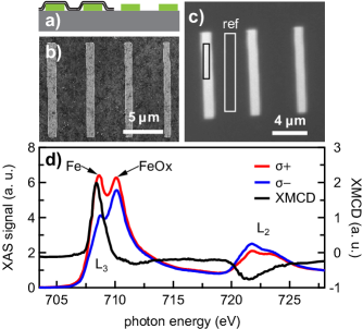
In Fig. 1 d) XAS at the Fe edge are shown for and polarized light in red and blue respectively. There are two main peaks corresponding to the spin-orbit splitting of the 2p core level, the L3 edge (E ) and L2 edge (E ). The two circularly polarized photons probe different transition probabilities into the spin-split 3d band and give rise to a magnetic contrast, which is given by the difference of the two XAS and is called XMCD: . The XMCD signal (black line) is positive at the L3 edge and negative at the L2 edge as expected since the average spin of the probing electron is inverted at the L2 edge compared to the L3 edge 1995_Stoehr . Two sub peaks at the L3 edge are observed in the as well as in the XAS signal. A large magnetic contrast is observed for the left peak, whereas the right peak only shows very weak magnetic contrast. Metallic iron gives rise to a strong magnetic contrast due to its ferromagnetic nature and therefore we ascribe the left peak to the Fe peak (E ). Iron can form many different oxides, FeO, Fe3O4, -Fe2O3 and -Fe2O3 for example. FeO and -Fe2O3 are antiferromagnetic and will not show any magnetic contrast. Fe3O4 as well as -Fe2O3 are ferrimagnetic and can contribute to a magnetic contrast, depending on the coupling to the ferromagnet below. Since -Fe2O3 has a spectral signature similar to Fe3O4 2011_Jimenez-Villacorta it is difficult to distinguish from the latter. Therefore, we do not discriminate between the two here. Furthermore, the XMCD signal in Fig. 1 d) shows a different line shape than expected for Fe3O4 and -Fe2O3 2004_Huang ; 2006_Kim . We conclude that the left peak can be ascribed to metallic Fe and the right peak (E ) can be ascribed to the iron oxides and therefore we will call the right peak the iron oxide peak.
III Results
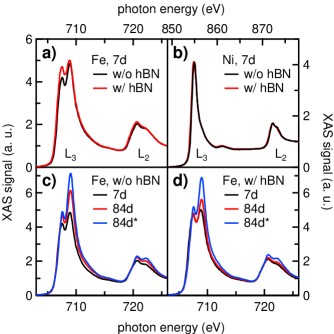
In order to investigate hBN as an oxidation barrier for ferromagnetic nano structures, the XAS of Py strips at the Fe and Ni edge were recorded after in ambient conditions (7d), after in ambient conditions (84d) and after an additional on a hotplate at in ambient conditions (84d*).
A direct comparison of the XAS of a covered (w/ hBN) and an uncovered (w/o hBN) Py strip at the Fe edge is shown in Fig. 2 a). The smaller iron peak at the L3 edge for the uncovered region indicates that there is a thicker oxide layer on top of the uncovered region (black curve) compared to the hBN covered (red). A similar, but smaller effect is also observed at the L2 edge of the iron. At the Ni edge, there is no noticeable difference between the two different regions and no sign of oxidation, see Fig. 2 b). Altogether, it is clear that there is a significant difference in iron oxidation in Py strips between hBN covered and uncovered regions.
The evolution of the XAS at the Fe edge with time is shown in Fig. 2 c) for an uncovered region and in d) for a hBN covered region. It is clear that in both cases the oxide peak grows with longer oxygen exposure time. Furthermore, the L2 resonance of Fe starts to split into two peaks as well, indicating further oxidation. However, it is also clear that the oxide peak of the hBN covered region grows slower, especially for the XAS at 84d.
To quantify the amount of oxidation for the different samples we modelled the XAS signal and fitted the measured spectra. For that we assumed that the metallic ferromagnet is covered with a layer of oxide on top. In the case of Py, we treated the iron and the nickel individually. This is justified by the relatively small Fe content of the Py that favours individual oxidation of the elements as supported by our data. In short, oxidised Fe is found to co-exist with metallic Ni in agreement with the higher oxygen affinity of Fe compared to Ni 1971_Reed .
In the case of iron, a layer of Fe2O3 with a thickness atop a layer of Fe3O4 with a thickness of atop a Fe layer of infinite thickness was assumed. FeO was neglected since it is only stable under conditions of limited oxygen availability (2001_Regan, ; 2014_Vaz, ). Since Fe2O3 is the higher oxidised state of iron, we assume that the best model structure is given in Fig. 3 c) where Fe2O3 is the topmost layer. Details about the fitting procedure can be found in the supporting information. We were unable to reasonably fit the measured data with a single oxide layer only. In Fig. 3 a) we show a fit to a measured XAS, showing excellent agreement. By fitting the XAS for all different conditions we are able to extract the individual oxide thicknesses, which are shown in Fig. 3 b). The error bars correspond to the standard deviations obtained from least square fits. The statistical error (variance between different regions) is smaller than the error obtained from the fitting and therefore the statistical contribution was neglected.
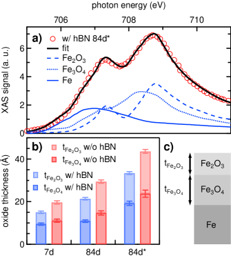
Our results show that the oxide is always significantly thinner for the hBN covered regions compared to uncovered regions, see Fig. 3 b). It is also obvious that both oxide layers increase in thickness with longer oxygen exposure time. This is the case for hBN covered and uncovered regions, but more significant for the uncovered regions. Whereas is similar for hBN covered and uncovered regions, the Fe2O3 layer is much thicker for the uncovered regions at . As the Py strips are further exposed to air (84 d), mainly increases with moderate changes in . The oxidation is promoted by putting the sample on a hotplate at as indicated by the increase in the oxide layer thickness and by a modification in the relative weight of the two oxides.
Similar to the Fe edge, the Ni L3 edge was used to extract the thickness of the NiO. Higher oxidation states of nickel were neglected since they only form at higher temperatures 2013_Liu . In Fig. 4 a) we show a fit to a measured XAS after in ambient conditions, showing also excellent agreement. The individual components are also shown in blue. The metallic Ni is dominating, indicating a thin NiO layer. By fitting the XAS for all different conditions, we were able to extract the individual oxide thicknesses, which are shown in Fig. 4 b).
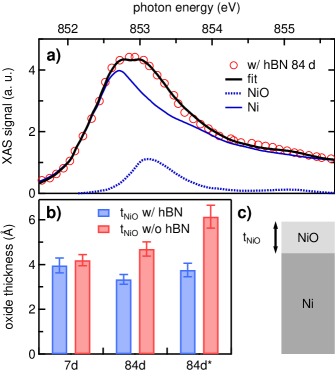
Initially, one finds no difference between hBN covered and uncovered regions in the oxidation of Ni, see Fig. 4 b) at . Upon further oxygen exposure, the thickness of the NiO stays the same within the error bars for hBN covered regions. In contrast to that, Ni oxidises further in the the case of uncovered Py strips and increases by to .
We have done a similar analysis for hBN covered and uncovered cobalt strips, where we extracted the thickness of the CoO (). Higher oxidation states of cobalt were neglected as in the Ni case. In Fig. 5 a) we show a fit to a measured XAS after in ambient conditions, showing excellent agreement. By fitting the XAS for all different conditions we are able to extract the individual oxide thicknesses, which are shown in Fig. 5 b).
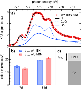
Although it is not obvious on first sight that Co strips covered with hBN oxidise more slowly, the absolute increase of is significantly smaller than the increase of for the uncovered region. It is important to note that markers on the samples allowed us to look at the same location in different measurements (e.g. 7d and 84d).
Table 1 and 2 show an overview of the extracted oxide thicknesses for the different elements and samples. The difference () is calculated by subtracting the oxide thickness with hBN from the oxide thickness without hBN.
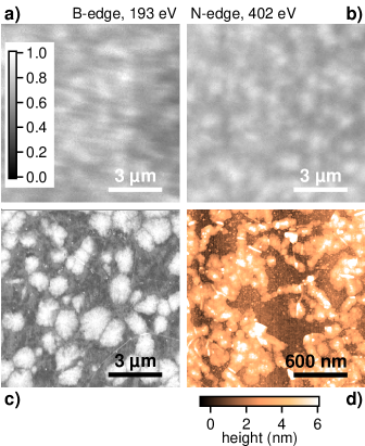
Since the hBN is a crucial part of this study, we characterised the hBN with several techniques, including PEEM, SEM and atomic force microscopy (AFM). PEEM images of hBN transferred on top of ferromagnetic strips are shown in Fig. 6 recorded at the boron K-edge (a)) and at the nitrogen K-edge (b)). Both images are edge / pre edge images where the image at the edge is divided by an image at the pre edge. This corrects for unwanted contributions from the detectors stage and it also corrects for surface effects such that the observed contrast is a pure material contrast. Furthermore, the intensity has been normalized. In both images, spatial intensity variations are clearly visible indicating an inhomogeneous hBN layer, largely varying in thickness. Similar structures are also observed in the SEM image (see Fig. 6 c)). This SEM image was taken on the as-received hBN on copper foil and therefore we conclude that this inhomogenities are not introduced by the transfer, but are rather a sign of a low quality hBN layer. AFM characterisation of an hBN layer transferred to a Si/SiO2 wafer shown in d) reveal height variations of around which are far from the thickness of a single layer (). From the observations, we conclude that the hBN layers have not only multilayer patches but may also have holes and cracks.
| () | () | |||||
|---|---|---|---|---|---|---|
| w/o hBN | w/ hBN | w/o hBN | w/ hBN | |||
| 7d | ||||||
| 84d | ||||||
| 84d* |
| () | () | |||||
|---|---|---|---|---|---|---|
| w/o hBN | w/ hBN | w/o hBN | w/ hBN | |||
| 7d | ||||||
| 84d | ||||||
| 84d* |
IV Discussion
Summarizing the data presented above, we can clearly say that there is a difference in oxidation of Fe and Ni for hBN covered and uncovered strips, namely that the hBN covered strips are less oxidised. This is most obvious when comparing the increase in oxide thickness from to oxygen exposure time.
Ni in close proximity to Fe clearly oxidises slowly and only a very thin oxide layer forms at the top. This can easily be explained by the fact that Fe oxidises first as it has a higher oxygen affinity than the Ni 1971_Reed . Ni will then only start to oxidise if all iron in close proximity is fully oxidised.
The thin oxide layer already present at for all samples is partially due to the fabrication process used here. After evaporation in vacuum, the strips are brought to ambient conditions for around for lift-off. This is already enough for the ferromagnetic materials to oxidise to a certain depth.
Treating the Py as pure Fe for the fitting of the Fe L3 edge probably underestimates the thicknesses of the oxides since only of the atoms in the Py are iron atoms. This might lead to extracted values that are smaller than in reality, but the change over time is still captured well. At the absorption edge of Ni, no Fe related features in absorption are expected, nor vice versa, since the energies of the photons are very different. Furthermore, the electron escape depth is similar for Fe ( = ) and Ni ( = ).
In the case of the Co strips, the protection of the hBN against oxidation is not obvious. The behaviour observed is attributed to the low quality of the hBN layers.
During the heat treatment at in ambient conditions, the relative weight of the two iron oxides is most probably changed due to different activation energy in their formation. The ratio of decreased with the heat treatment indicating a shift towards Fe3O4. In addition, an increased temperature also leads to a faster oxygen diffusion within the Py strip. This might be the reason why there is more Fe3O4 after the hotplate treatment.
We have also seen an increase in the oxide thickness for the Fe and Co in the hBN covered regions, although it is less pronounced. A defective layer of hBN with some holes or cracks would surely allow for some oxygen diffusion through the layer. In addition, grain boundaries could also allow oxygen diffusion through the layer. These two issues are related to the quality of the hBN and could be minimized by a higher quality hBN (e.g. more homogeneous layer and larger crystals). The mechanical transfer of the hBN on top of the ferromagnetic strips could also lead to cracks along the edges of the strips. This is possible since the height of the strips () greatly exceeds the hBN thickness and therefore the hBN could rupture along this step edge. Heating the sample to elevated temperature could even promote this rupturing since the different materials involved have different thermal expansion coefficients. Moreover, oxygen diffusion along the hBN / SiO2 interface is possible, even though long distances have to be overcome. A defective hBN layer would facilitate the diffusion along the interface since the distances can be orders of magnitude smaller.
To sum up, the quality and the ex-situ transfer of hBN on top of the ferromagnetic material limits the effective protection of the hBN. This could possibly be solved by an in-situ transfer of high quality hBN onto pre-patterned and pre-cleaned ferromagnetic electrodes (e.g. transfer in an UHV system with sputter cleaned ferromagnets). Even more attractive is the direct CVD growth of hBN on predefined ferromagnetic strips. Recently, large single crystal CVD growth of hBN on a Fe catalyst has been achieved 2015_Caneva , paving the way for hBN protected iron strips.
V Conclusion
We conclude that the hBN slows down the oxidation of permalloy nanostructures. However, the ex-situ transfer of hBN has its limitations as the ferromagnetic materials are shortly exposed to air which is enough to oxides ferromagnetic surfaces several atomic layers deep. These mostly antiferromagnetic oxide layers might substantially decrease the spin-polarization of the electrons in electrical spin injection experiments. Most probably, in-situ grown hBN on ferromagnetic contacts could be a better solution for spin injectors into non-magnetic materials such as graphene as it most probably would protect the ferromagnetic material from oxidation. In addition this hBN coating could serve as a perfect tunnel barrier for electrical spin injection. Further investigations with higher quality hBN layers need to be done to clarify the performance of hBN as a potential oxidation barrier for ferromagnetic nanostructures.
VI Acknowledgements
The authors gratefully thank Gulibusitan Abulizi for the atomic force microscopy picture of the hBN. We also thank Armin Kleibert and Frithjof Nolting for fruitful discussions. Part of this work was performed at the Surface/Interface: Microscopy (SIM) beam line of the Swiss Light Source, Paul Scherrer Institut, Villigen, Switzerland. This work was further funded by the Swiss National Science Foundation, the Swiss Nanoscience Institute, the Swiss NCCR QSIT, the ERC Advanced Investigator Grant QUEST and the EU Flagship project graphene.
References
- [1] Igor Žutić, Jaroslav Fabian, and S. Das Sarma. Spintronics: Fundamentals and applications. Rev. Mod. Phys., 76:323–410, Apr 2004.
- [2] Wei Han, Roland K. Kawakami, Martin Gmitra, and Jaroslav Fabian. Graphene spintronics. Nat Nano, 9(10):794–807, October 2014.
- [3] P. Seneor, B. Dlubak, M.-B. Martin, A. Anane, H. Jaffres, and A. Fert. Spintronics with graphene. MRS Bulletin, 37:1245–1254, 12 2012.
- [4] T. Miyazaki and N. Tezuka. Giant magnetic tunneling effect in Fe/Al2O3/Fe junction. Journal of Magnetism and Magnetic Materials, 139(3):L231 – L234, 1995.
- [5] J. S. Moodera, Lisa R. Kinder, Terrilyn M. Wong, and R. Meservey. Large Magnetoresistance at Room Temperature in Ferromagnetic Thin Film Tunnel Junctions. Phys. Rev. Lett., 74:3273–3276, Apr 1995.
- [6] G. Schmidt, D. Ferrand, L. W. Molenkamp, A. T. Filip, and B. J. van Wees. Fundamental obstacle for electrical spin injection from a ferromagnetic metal into a diffusive semiconductor. Phys. Rev. B, 62:R4790–R4793, Aug 2000.
- [7] Xinran Wang, Scott M. Tabakman, and Hongjie Dai. Atomic Layer Deposition of Metal Oxides on Pristine and Functionalized Graphene. Journal of the American Chemical Society, 130(26):8152–8153, 2008. PMID: 18529002.
- [8] W. H. Wang, W Han, K Pi, K. M. McCreary, F. Miao, W. Bao, C. N. Lau, and R. K. Kawakami. Growth of atomically smooth MgO films on graphene by molecular beam epitaxy. Applied Physics Letters, 93:183107, 2008.
- [9] Kenji Watanabe, Takashi Taniguchi, and Hisao Kanda. Direct-bandgap properties and evidence for ultraviolet lasing of hexagonal boron nitride single crystal. Nat Mater, 3(6):404–409, June 2004.
- [10] Gwan-Hyoung Lee, Young-Jun Yu, Changgu Lee, Cory Dean, Kenneth L. Shepard, Philip Kim, and James Hone. Electron tunneling through atomically flat and ultrathin hexagonal boron nitride. Applied Physics Letters, 99(24):243114, 2011.
- [11] Liam Britnell, Roman V. Gorbachev, Rashid Jalil, Branson D. Belle, Fred Schedin, Mikhail I. Katsnelson, Laurence Eaves, Sergey V. Morozov, Alexander S. Mayorov, Nuno M. R. Peres, Antonio H. Castro Neto, Jon Leist, Andre K. Geim, Leonid A. Ponomarenko, and Kostya S. Novoselov. Electron Tunneling through Ultrathin Boron Nitride Crystalline Barriers. Nano Letters, 12(3):1707–1710, 2012.
- [12] F. Amet, J. R. Williams, A. G. F. Garcia, M. Yankowitz, K. Watanabe, T. Taniguchi, and D. Goldhaber-Gordon. Tunneling spectroscopy of graphene-boron-nitride heterostructures. Phys. Rev. B, 85:073405, Feb 2012.
- [13] U. Chandni, K. Watanabe, T. Taniguchi, and J. P. Eisenstein. Evidence for Defect-Mediated Tunneling in Hexagonal Boron Nitride-Based Junctions. Nano Letters, 15(11):7329–7333, 2015. PMID: 26509431.
- [14] Takehiro Yamaguchi, Yoshihisa Inoue, Satoru Masubuchi, Sei Morikawa, Masahiro Onuki, Kenji Watanabe, Takashi Taniguchi, Rai Moriya, and Tomoki Machida. Electrical Spin Injection into Graphene through Monolayer Hexagonal Boron Nitride. Applied Physics Express, 6(7):073001, 2013.
- [15] Wangyang Fu, Péter Makk, Romain Maurand, Matthias Bräuninger, and Christian Schönenberger. Large-scale fabrication of BN tunnel barriers for graphene spintronics. Journal of Applied Physics, 116(7):074306, 2014.
- [16] M. Venkata Kamalakar, André Dankert, Johan Bergsten, Tommy Ive, and Saroj P. Dash. Enhanced Tunnel Spin Injection into Graphene using Chemical Vapor Deposited Hexagonal Boron Nitride. Sci. Rep., 4, August 2014.
- [17] Oleg V. Yazyev and Alfredo Pasquarello. Magnetoresistive junctions based on epitaxial graphene and hexagonal boron nitride. Phys. Rev. B, 80:035408, Jul 2009.
- [18] André Dankert, M. Venkata Kamalakar, Abdul Wajid, R.S. Patel, and Saroj P. Dash. Tunnel magnetoresistance with atomically thin two-dimensional hexagonal boron nitride barriers. Nano Research, 8(4):1357–1364, 2015.
- [19] M.-B. Martin, B. Dlubak, R. S. Weatherup, M. Piquemal-Banci, H. Yang, R. Blume, R. Schloegl, S. Collin, F. Petroff, S. Hofmann, J. Robertson, A. Anane, A. Fert, and P. Seneor. Protecting nickel with graphene spin-filtering membranes: A single layer is enough. Applied Physics Letters, 107(1):012408, 2015.
- [20] Zheng Liu, Yongji Gong, Wu Zhou, Lulu Ma, Jingjiang Yu, Juan Carlos Idrobo, Jeil Jung, Allan H. MacDonald, Robert Vajtai, Jun Lou, and Pulickel M. Ajayan. Ultrathin high-temperature oxidation-resistant coatings of hexagonal boron nitride. Nat Commun, 4, October 2013.
- [21] Xuemei Li, Jun Yin, Jianxin Zhou, and Wanlin Guo. Large area hexagonal boron nitride monolayer as efficient atomically thick insulating coating against friction and oxidation. Nanotechnology, 25(10):105701, 2014.
- [22] X M Cheng and D J Keavney. Studies of nanomagnetism using synchrotron-based x-ray photoemission electron microscopy (X-PEEM). Reports on Progress in Physics, 75(2):026501, 2012.
- [23] T. J. Regan, H. Ohldag, C. Stamm, F. Nolting, J. Lüning, J. Stöhr, and R. L. White. Chemical effects at metal/oxide interfaces studied by x-ray-absorption spectroscopy. Phys. Rev. B, 64:214422, Nov 2001.
- [24] C. A. F. Vaz, A. Balan, F. Nolting, and A. Kleibert. In situ magnetic and electronic investigation of the early stage oxidation of Fe nanoparticles using X-ray photo-emission electron microscopy. Phys. Chem. Chem. Phys., 16:26624–26630, 2014.
- [25] J. Stöhr. X-ray magnetic circular dichroism spectroscopy of transition metal thin films. Journal of Electron Spectroscopy and Related Phenomena, 75:253 – 272, 1995.
- [26] F. Jiménez-Villacorta, C. Prieto, Y. Huttel, N. D. Telling, and G. van der Laan. X-ray magnetic circular dichroism study of the blocking process in nanostructured iron-iron oxide core-shell systems. Phys. Rev. B, 84:172404, Nov 2011.
- [27] D. J. Huang, C. F. Chang, H.-T. Jeng, G. Y. Guo, H.-J. Lin, W. B. Wu, H. C. Ku, A. Fujimori, Y. Takahashi, and C. T. Chen. Spin and Orbital Magnetic Moments of Fe3O4. Phys. Rev. Lett., 93:077204, Aug 2004.
- [28] J.-Y. Kim, T. Y. Koo, and J.-H. Park. Orbital and Bonding Anisotropy in a Half-Filled Magnetoelectric Ferrimagnet. Phys. Rev. Lett., 96:047205, Jan 2006.
- [29] T. B. Reed. Free Energy of Formation of Binary Compounds. The MIT Press, Cambridge, MA, 1971.
- [30] Sabina Caneva, Robert S. Weatherup, Bernhard C. Bayer, Barry Brennan, Steve J. Spencer, Ken Mingard, Andrea Cabrero-Vilatela, Carsten Baehtz, Andrew J. Pollard, and Stephan Hofmann. Nucleation Control for Large, Single Crystalline Domains of Monolayer Hexagonal Boron Nitride via Si-Doped Fe Catalysts. Nano Letters, 15(3):1867–1875, 2015. PMID: 25664483.