Compound structure one-dimensional photonic crystal
Abstract
In this paper, we have proposed a new compound structure one-dimensional photonic crystal, which include series connection, parallel connection and positive and negative feedback compound structure photonic crystal. We have studied their transmission characteristics and obtained some new results, which should be help to design new type optical devices, such as optical amplifier, photonic crystal laser and so on.
PACS: 41.20.Jb, 42.70.Qs, 78.20.Ci
Keywords: photonic crystals; transmissivity; series connection;
parallel connection; positive and negative feedback
1. Introduction In 1987, E. Yablonovitch and S. John had pointed out that the behavior of photons can be changed when propagating in the material with periodical dielectric constant, and termed such material Photonic Crystal [1, 2]. Photonic crystal important characteristics are: Photon Band Gap, defect states, Light Localization and so on. These characteristics make it able to control photons, so it may be used to manufacture some high performance devices which have completely new principles or can not be manufactured before, such as high-efficiency semiconductor lasers, right emitting diodes, wave guides, optical filters, high-Q resonators, antennas, frequency-selective surface, optical wave guides and sharp bends [3, 4], WDM-devices [5, 6], splitters and combiners [7, 8]. optical limiters and amplifiers [9, 10]. The research on photonic crystals will promote its application and development on integrated photoelectron devices and optical communication. To investigate the structure and characteristics of band gap, there are many methods to analyze Photonic crystals including the plane-wave expansion method [11], Green s function method, finite-difference time-domain method [12-14] and transfer matrix method [15-17].
In the paper, we have proposed a new compound structure one-dimensional photonic crystal, which include series connection, parallel connection and positive and negative feedback compound structure photonic crystal. We have given their transmission coefficients and transmissivities, studied their transmission characteristics and obtained some new results: (1) The forbidden band width of series connection photonic crystal becomes more wider, and it is the union of corresponding forbidden band of part photonic crystal, which is similar as the series connection ohm law in circuit. (2) We can obtain the more wider forbidden band by photonic crystal series connection. (3) With the number of series connection photonic crystal increasing, the total width of forbidden band increase. (4) The total forbidden band width of parallel connection photonic crystal is adjusted by superposition coefficient. (5) For the positive and negative feedback, the transmissivity are larger than , which can achieve light amplification in the positive and negative feedback photonic crystal. All these results should be help to design new type optical devices, such as optical amplifier, photonic crystal laser and so on.
2. Transfer matrix and transmissivity of one-dimensional photonic crystal
For one-dimensional conventional PCs, the calculations are performed using the transfer matrix method [18], which is the most effective technique to analyze the transmission properties of PCs. For the medium layer , the transfer matrices for wave is given by [18]:
| (3) |
where , is speed of light in vacuum, is the ray angle inside the layer with refractive index , , , in which is the refractive index of the environment wherein the incidence wave tends to enter the structure, and is the incident angle.
The total transfer matrix for an period structure is given by:
| (8) | |||||
| (15) |
where
| (18) |
with the total transfer matrix , we can obtain the transmissivity , it is
| (19) |
Where . By the Eqs. (1) and (4), we can calculate the transmissivity of one-dimensional photonic crystal.
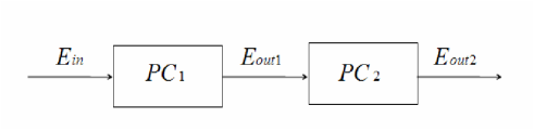
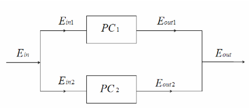
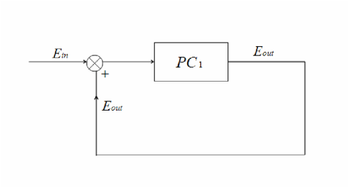
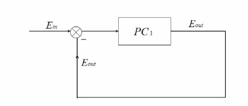
3. Series connection, parallel connection and feedback one-dimensional photonic crystal transmissivity Two or multiple one-dimensional photonic crystal can be connected by optical fiber, which can be designed series connection, parallel connection and feedback compound structure one-dimensional photonic crystal. The FIGs. 1, 2, 3 and 4 are series connection, parallel connection, positive feedback and negative feedback one-dimensional photonic crystal structures, respectively. The and are two kinds one-dimensional photonic crystal, is the input electric field intensity, and and are the output electric field intensity of and .
(1) The total transmission coefficient and transmissivity of series connection one-dimensional photonic crystal are
| (20) |
| (21) |
where and for the transmission coefficients of photonic crystals and .
Similarly, the total transmission coefficient for photonic crystals , , , series connection is
| (22) |


(2) The total transmission coefficient and transmissivity of parallel connection one-dimensional photonic crystal are
| (23) |
when and phase are the same (opposite), the numerator of Eq. (8) takes ().
when , there are
| (24) |
where and .
when , there is
| (25) |
Similarly, the total transmission coefficient of photonic crystals , , , parallel connection is
| (26) | |||||
(3) We can calculate the total transmission coefficient and transmissivity of positive feedback one-dimensional photonic crystal.
The output of first times positive feedback is
| (27) |
the output of second times positive feedback is
| (28) |
the transmission coefficient of second times positive feedback is
| (29) |
the output of third times positive feedback is
| (30) |
the transmission coefficient of third times positive feedback is
| (31) |
similarly, the transmission coefficient of times positive feedback is
| (32) |
finally, we can obtain the limit transmission coefficient of positive feedback, it is
| (33) |
(4) We can calculate the total transmission coefficient and transmissivity of negative feedback one-dimensional photonic crystal.
The output of first times negative feedback is
| (34) |
the output of second times negative feedback is
| (35) |
the transmission coefficient of second times negative feedback is
| (36) |
the output of third times negative feedback is
| (37) |
the transmission coefficient of third times negative feedback is
| (38) |
similarly, the transmission coefficient of times negative feedback is
| (39) |
finally, we can obtain the limit transmission coefficient of negative feedback, it is
| (40) |


4. Numerical result
In this section, we report our numerical results of compound structure one-dimensional photonic crystal, the two kinds of photonic crystal and , their structures are and , respectively. The main parameters are: The center angle wavelength , the medium refractive indices , thickness , the medium refractive indices , thickness , the medium refractive indices , thickness , the medium refractive indices , thickness . Firstly, we study the series connection structure photonic crystal, which is constituted by and , it is shown in FIG. 1. The series connection structure is referred to as . From Eqs. (5) and (6), we can calculate the series connection structure transmissivity. The FIG. 5 (a), (b) and (c) are the transmissivity corresponding to the structure , and . From FIG. 5 (a), (b) and (c), we can obtain some results: (1) The forbidden band width of series connection photonic crystal becomes more wider, and it is the union of corresponding forbidden band of part photonic crystal and , which is similar as the series connection ohm law in circuit. (2) We can obtain the more wider forbidden band by photonic crystal series connection. (3) With the number of series connection photonic crystal increasing, the total width of forbidden band increase. In FIG. 6, the photonic crystal with defect layer, its structure is , the defect medium parameters are: refractive indices , thickness . There is a defect model in FIG. 6 (a). When the and constitute series connection structure photonic crystal , its forbidden band width is the union of corresponding forbidden band of and , and the defect model disappears, since the defect model is in the forbidden band range of and . In FIG. 7, we change the thickness of , it is , the position of forbidden band red-shift. When the and constitute series connection structure photonic crystal , its forbidden band width is the union of corresponding forbidden band of and , the forbidden band width increases obviously. There is a defect model in series connection photonic crystal forbidden band, it is because there is a little conduction band overlap of and in forbidden band. Secondly, we study the parallel connection structure photonic crystal, which is constituted by and , it is shown in FIG. 2. The parallel connection structure is referred to as . By Eq. (10), we can calculate the parallel connection structure transmissivity . The FIG. 8 (a) and (b) are the transmissivity of and , and (c), (d) and (e) are the transmissivity of parallel connection corresponding coefficient is , and , respectively. We can obtain some results: (1) When coefficient the transmissivity of parallel connection (FIG. 8 (c)) is close to the transmissivity of (FIG. 8 (b)). (2) When coefficient the transmissivity of parallel connection (FIG. 8 (d)) is close to the transmissivity of (FIG. 8 (a)). (3) When coefficient the forbidden band of parallel connection (FIG. 8 (e)) is the intersection of corresponding forbidden band of and . Finally, we study the positive and negative feedback structure photonic crystal, which is constituted by , it is shown in FIGs. 3 and 4. The positive and negative feedback structure is referred to as and , respectively. From Eqs. (12) to (18), we can calculate the positive feedback structure transmissivity. The FIG. 9 (a) is the transmissivity of , (b), (c), (d) and (e) are the transmissivity of the first time, the second time, the third time and the limit positive feedback, respectively. We can obtain some results: (1) There are the same forbidden band width for the first time, the second time, the third time and the limit positive feedback. (2) From the first times positive feedback, the transmissivity is larger than , which can achieve light amplification in positive feedback. (3) With the increasing of feedback times, the amplitude of transmissivity increases. From Eqs. (19) to (25), we can calculate the negative feedback structure transmissivity. The FIG. 10 (a) is the transmissivity of , (b), (c), (d) and (e) are the transmissivity of the first time, the second time, the third time and the limit negative feedback, respectively. We can obtain some results: (1) There are the same forbidden band width for the first time, the second time, the third time and the limit negative feedback. (2) From the first times negative feedback, the transmissivity is larger than , which can achieve light amplification in negative feedback. (3) With the increasing of feedback times, the amplitude of transmissivity increases. The FIGs. 11 and 12 are the positive and negative limit feedback maximum transmissivity. We can obtain some results: (1) At , the positive limit feedback maximum transmissivity . At , the negative limit feedback maximum transmissivity , there are the extremely strong output light intensity, which can be designed into the photonic crystal laser. (2) The positive and negative feedback photonic crystal both can achieve the light amplification, which is different from the electronic positive and negative feedback system, only the electronic positive system can achieve the electrical signal amplification.
5. Conclusion
In summary, we have proposed a new compound structure one-dimensional photonic crystal, which include series connection, parallel connection and positive and negative feedback compound structure photonic crystal. We have calculated their transmission characteristics and obtained some new results: (1) The forbidden band width of series connection photonic crystal becomes more wider, and it is the union of corresponding forbidden band of part photonic crystal, which is similar as the series connection ohm law in circuit. (2) We can obtain the more wider forbidden band by photonic crystal series connection. (3) With the number of series connection photonic crystal increasing, the total width of forbidden band increase. (4) The total forbidden band width of parallel connection photonic crystal is adjusted by superposition coefficient. (5) For the positive and negative feedback, the transmissivity are larger than , which can achieve light amplification in the positive and negative feedback photonic crystal. (6) At , the positive limit feedback maximum transmissivity . At , the negative limit feedback maximum transmissivity , there are the extremely strong output light intensity, which can be designed into the photonic crystal laser. All these results should be help to design new type optical devices, such as optical amplifier, photonic crystal laser and so on.
6. Acknowledgment
This work is supported by Scientific and Technological Development Foundation of Jilin Province, Grant Number: 20130101031JC.
References
- (1) E. Yablonovitch, Phys. Rev. Lett. 58, 2059 (1987).
- (2) S. John, Phys. Rev. Lett. 58 2486 (1987).
- (3) A. Lavrinenko, P.I. Borel, L.H. Frandsen, M. Thorhauge, A. Harpth, M. Kristensen, T. Niemi, Opt. Express 12 234 (2004).
- (4) J. Pu, Y. Yomogida, K. K. Liu, L. J. Li, Y. Iwasa, and T. Takenobu, Nano Lett., 12 4013, (2012).
- (5) S. Fan, P.R. Villeneuve, J.D. Joannopoulos, H.A. Haus, Phys. Rev. Lett. 80 960 (1998).
- (6) A. Ferreira, N. M. R. Peres, R. M. Ribeiro and T. Stauber, Phys. Rev. B, 85 115438, (2012).
- (7) S. Kim, I. Park, H. Lim, Proc. Design of photonic crystal splitters/combiners SPIE 5597 129 (2004).
- (8) N. M. R. Peres and Yu. V. Bludov, EPL, 101 58002, (2013).
- (9) R. Martinez-Sala, J. Sancho, J. V. Sanchez, V. Gomez, J. Llinares and F. Meseguer, nature 378, 241 (1995).
- (10) T. Cai, R. Bose, G. S. Solomon, and E. Waks, Appl. Phys. Lett. 102 141118 (2013).
- (11) J. J. Joannopoulos, R. D. Meade, J. N. Winn, Photonic crystals: molding the flow of light (Princeton University Press, New Jersey, 1995).
- (12) M. Minkov and V. Savona, Phys. Rev. B 88 081303R (2013).
- (13) K. K. Yee, IEEE Trans. Antennas Propag. 14, 302 (1966).
- (14) K. S. Choi, H. Deng, J. Laurat, and H. J. Kimble, Nature 452, 67 (2006).
- (15) J. B. Pendry, Phys. Rev. Lett. 69, 2772 (1992).
- (16) M. Jachura, M. Karpinski, C. Radzewicz, and K. Banaszek, Opt. Express 22 8624 (2014).
- (17) D. A. Miller, Nature Photonics 4 3 (2010).
- (18) J. Zi, J. wan and C. Zhang, Appl. Phys. Lett, 73, 2084 (1998).