Near-field properties of plasmonic nanostructures with high aspect ratio
Y. Ould Agha1, O. Demichel1, C. Girard2 A. Bouhelier1 and G. Colas des Francs1
1Laboratoire Interdisciplinaire Carnot de Bourgogne (ICB)
UMR 6303 CNRS/Université de Bourgogne
9, Av. Savary, BP 47870, 21078 Dijon Cedex, France
2Centre d’Elaboration de Matériaux et d’Etudes Structurales (CEMES)
CNRS, 29 rue J. Marvig F-31055 Toulouse, France
Abstract— Using the Green’s dyad technique based on cuboidal meshing, we compute the electromagnetic field scattered by metal nanorods with high aspect ratio. We investigate the effect of the meshing shape on the numerical simulations. We observe that discretizing the object with cells with aspect ratios similar to the object’s aspect ratio improves the computations, without degrading the convergency. We also compare our numerical simulations to finite element method and discuss further possible improvements.
Keywords: Dyadic Green Method; Finite element method; Metallic nanoscatterer; Surface plasmon resonance;
1 Introduction
Plasmonic nanostructures concentrate light on subwavelength scales [1, 2], opening the way to promising applications such as nano-optical antennas [3, 4], or surface enhanced spectroscopies [5, 6]. In the last decade, important efforts have been done in modeling these structures [7]. Particularly, the electric field rapidly decays away from the metal surface so that dedicated methods have to be developed to correctly describe near-field optics properties of plasmonic systems. Additionnally, high aspect ratio shapes are often needed to tune resonance frequencies [8, 9]. Fast field decay and high aspect ratio lead to serious numerical difficulties for methods based on the discretization of the object volume, notably in term of memory cost and computational time.
We are specifically interested in the Green’s dyad technique (GDT) (also called volume integral method) [10] since it naturally satisfies boundary conditions both at the object surfaces and in the far-field. Moreover, it easily includes a substrate supporting nanoparticles without the need to discretize it [11]. In addition, as far as the Green’s dyadic is numerically computed in the source (nanostructures) region, all the electromagnetic properties of the system are easily obtained with practically almost no additionnal computing cost [12]. This concerns obviously the electric and magnetic fields in the very near-field of the object [13] but also scattering properties in the radiation zone [14, 15]. Last, the local density of optical states (LDOS), an intrinsic property of the nanostructure, is also easily deduced from this formalism [16].
Recent works were devoted to improve the GDT when applied to metallic nanostructures. The GDT relies on the discretization of the scatterers. Because of strongly varying fields, the key point is to correctly describe the fast variation of the Green’s tensor over an elementary cell. Let us mention the regularization scheme proposed by Kottmann and Martin developed for 2D-elements but also transposable to 3D-nanostructures [17]. Instead of regularizing the Green’s tensor, Chaumet and coworkers directly computed its integral over the volume of cubic meshes [18]. To this aim, they considered a Weyl expansion of the tensor and performed a numerical integration in the reciprocical k-space. In the present work, we first transform the volume integral to a surface integral over a cuboidal mesh [19] before a numerical evaluation in direct space. This avoids the singularity at the mesh center and convergence difficulties. Moreover, this permits to consider more complex meshing. Note finally that our method differs from surface integral method (also called boundary element method) where the object surface is discretized, including the substrate if necessary [20, 21, 22]. Surface integral method relies on the introduction of equivalent surface currents that depends on the excitation field. Differently, the volume integral method relies on a volume discretization of the object, excluding the substrate, but in the present work involves integration over the surface of the meshes. This leads to the evaluation of the Green’s dyad associated to the whole structure that is independent on the illumination conditions so that various problem can be treated by post-processing.
In the following, we define a benchmark configuration that consists of a silver nanorod. In order to assess the reliability of our results, we compare our numerical simulations to those obtained using a commercial software (COMSOL Multiphysics) based on the finite element method (FEM) [23]. The objective of this comparison is twofold. FEM efficiently considers complex shape but necessitates a careful design and positioning of a perfectly matched layer (PML) to avoid artefact reflexion at the boundaries of the computational window. As we will see, it becomes a very sensitive parameter in presence of a substrate. On the opposite, GDT easily considers nanostructures deposited on a substrate but is generally limited to simpler shapes. By comparing the two methods, we are able to estimate the error. Reciprocally, this validates the choice of the PML included in the FEM calculations.
2 Numerical methods
2.1 Green’s dyadic technique
We consider an object immersed in a homogeneous background medium. The addition of a substrate will be discussed later. The object and background are assumed nonmagnetic () with a relative permittivity, and , respectively. In the following, we assume an time harmonic dependence for the fields. The Green’s dyad represents the electromagnetic response to an elementary excitation. Physically, the electric field scattered at the position in presence of a point-like dipolar source located at follows
| (1) |
where is the free-space permittivity, the free-space wavenumber and is the Green’s tensor associated with the whole system. It is an intrinsic electromagnetic quantity of the object, independent on the excitation process. For instance the local density of mode is given by [24, 25]
| (2) |
In addition, if the object is excited by an incident electric field , the electric field can be expressed everywhere in the system by a 3D integral
| (3) |
with . Finally, the main numerical task is the evaluation of the tensor for every couple of points . The Green’s tensor can be computed by solving the self-consistent Dyson’s equation
| (4) |
where is the free-space Green’s dyad, that is analytical. In order to solve Dyson’s equation (4), the object is discretized into cells of volume ();
| (5) | |||
| (6) |
Depending on the object shape, different meshes can be used. In case of spherical cells, the integral of the Green’s tensor over a sphere of radius , centered at is analytical and writes [19]
| (7) | |||
| (8) |
is a geometrical factor that reduces to the sphere volume of subwavelength size (). In this case, the discretized Dyson’s equation 5 reduces to [7, 10]
| (9) |
However, when plasmonic objects with high aspect ratio are considered, it is preferable to use elongated cells. And the volume integral Eq. 6 has to be numerically evaluated. This is rather difficult because of the singularity of the Green’s tensor that occurs when the source and the observation points coincide () [26]. In a smilar context, Chaumet et al used a Weyl expansion of the Green’s tensor to performed the numerical integration of Eq. 6 in the reciprocical k-space [18]. More recently, Massa and cowokers derived an approximate analytical expression for the polarisability of a cuboidal cell [27].
In the present work, we first transform the volume integral to a surface integral over the (cuboidal) cell surface before a numerical evaluation in direct space. This avoids the singularity at the cell center and convergence difficulties.
In 2005, Gao et al demonstrated that this volume integral can be converted into a (flux) surface integral thanks to Ostrogradsky’s theorem [19]
| (10) |
where if the observation point is within the integration volume ) and is null elsewhere. For a rectangular parallelepiped mesh (), centered at the point , the surface integral term writes for instance
| (11) | |||
| (12) |
with and refers to either (plus sign) or (minus sign). Such surface integral is efficiently numerically computed using the Gauss-Kronrod method. The singularity of the Green’s dyad in the source region is properly taken into account in this approach. Another notable advantage of this approach is that it considerably reduces the memory cost for evaluating the Green’s dyadic. Finally, different mesh shapes can be considered by adapting the integral surface. And Dyson’s equation (Eq. 5) is numerically solved using standard matrix inversion techniques.
2.2 Finite element method
The finite element method is a common numerical tool to study problems related to electromagnetism. Its main advantage is that it can be applied to irregular geometries. Since a detailed description can be found in Ref. [28], only a brief introduction will be given here. In classical electromadynamics, FEM is typically used to solve problems governed by Maxwell’s equations that can be formulated as a vector wave equation for the electric field
| (13) |
The finite element method is based on the discretization of the whole geometry, including the surrounding medium, by simple elements (such as triangles in two dimensional problems, or tetrahedral elements in three dimensional problems). The system of equations to be solved can be assembled after obtaining the weak formulation of the partial differential equations.
However, one of the main difficulties in the finite element analysis of wave problems in open space is to truncate the unbounded domain. A common approach is to introduce a special layer of finite thickness surrounding the region of interest such that it is non-reflecting and completely absorbing for the waves entering this layer under any incidence. Such regions were introduced by Berenger and are called perfectly matched layers (PML) [29]. The most natural way is to consider PML as a geometrical transformation that leads to equivalent and (that are complex, anisotropic, and inhomogeneous even if the original ones were real, isotropic, and homogeneous) [30, 31] . This leads automatically to an equivalent medium with the same impedance than the one of the initial ambient medium since and are transformed in the same way. The equivalent and ensure that the interface with the layer is non-reflecting.
3 results and discussion
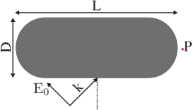
In the following, we consider a silver nanorod that consists of a cylinder rod capped with hemispherical ends (see Fig. 1). The diameter of the nanorod is and the total length is so that its aspect ratio is . In this part of our numerical model, the silver nanorod is immersed in air. We use the silver dielectric function tabulated by Johnson and Christy [32].
We first investigate the near field optical response of the silver nanorod using FEM. The PML parameters (thickness and position) were determined by benchmarking the calculation of a well-known object characterized by the exact generalized Mie theory [33] (not shown). Considering dimer test structures, we achieve an excellent agreement with thick spherical PML located at from the nanostructure. We then consider the silver nanorod presented in Fig. 1. A simple way to determine all the supported modes of the nanostructure is to excite it with an oblique incident plane wave . We characterize the optical near-field response by computing the electric field intensity at one extremity (point in Fig. 1).
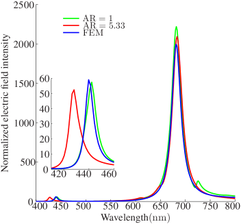
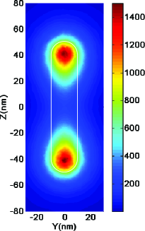
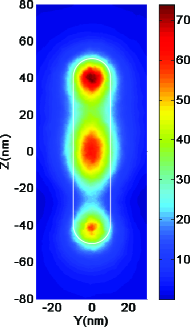
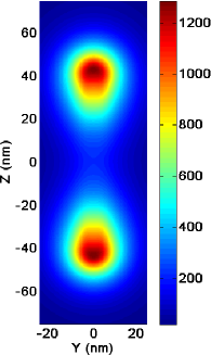
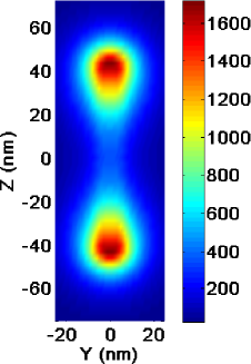
Figure 2 displays the near-field intensity spectra of the silver nanorod ( nm and nm). We observe two surface plasmon polariton (SPP) resonances located around and . These resonances are in agreement with a Fabry-Perot resonator description [34, 35, 36]. The effective indices of the SPP guided along a 20 nm silver nanowire are and at and , respectively. The cavity modes correspond to resonator lengths with is the mode order and refers to the field penetration depth into air. We obtain ] and for the two first modes. Note that these values for reveal that high order modes are strongly confined [2]. Figures 2 and 2 represent near-field intensity maps computed at these resonances located at and , respectively. The intensity map at nm is not symmetric due to an interference with the incident excitation field (Fig. 2). The apparent symmetry observed at nm is simply due to the fact that the amplitude of the excited mode is stronger than the incident field (Fig. 2).
We now apply the formalism of Green’s method presented in the previous section. The silver nanorod is discretized with rectangular parallelepipeds of dimensions . We set and equal to in the following, while varying the parameter from to as shown in Fig. 3. The two hemispherical caps are discretized with for each case. Only the central cylindrical part of the nanorod is meshed with different values. We use a transitory meshing area between the cap and the central part. The background is not discretized contrary to FEM calculations.
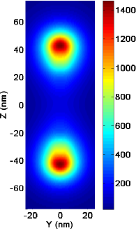
The near-field spectrum is calculated in Fig. 2 for two mesh aspect ratios, namely () and (). We observe an excellent agreement with the FEM calculated spectrum for the finer discretization, except for a peak near . This peak disappears when changing the meshing size so that it is easily detected as a numerical artefact. In case of meshing aspect ratio , the dipolar resonance () is in agreement with the FEM computation. The resonance is however slightly blue shifted. We represent the calculated intensity at in Fig. 3 for mesh aspect ratio ranging from 1 to 8. When the aspect ratio of elementary cells is close to the one of the full object (Fig. 3(c), ) we can reach a very good agreement with the result obtained by the finite element method (Fig.2).
| Aspect ratio | 1 | 2 | 5.33 | 8 |
| Number of cells | 1944 | 1112 | 696 | 488 |
| Computational time | 3h13min | 1h43min | 1h04min | 48min |
Table 1 indicates the number of meshing elements and the computing time for the different aspect ratios considered here. The computing time linearly increases with the cell number since the limiting operation is the numerical integration of the free-space Green’s tensor over the cuboidal cell (instead of an increasing time as when the limiting factor is the resolution of the self consistent Dyson’s equation 5).
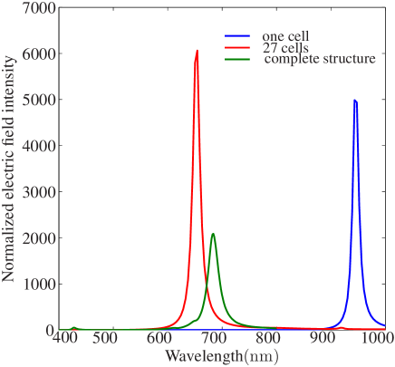
Apart from the finest meshing, we obtain the better result for a meshing shape concomitant with the full object aspect ratio (Fig. 3(c)). We attribute this to the fact that the resonance position of an elementary mesh is close to the object resonance. So the optical response of the whole structure is qualitatively described by the meshing and the object discretization refines the modelisation with a scaling law improvement. Figure 4 represents the near-field intensity when considering a single cell (AR=5.33), 27 cells (AR=5.33) or the full object (AR=5). Although the localized plasmon resonance of a silver spherical or cubic nanoparticle is around nm, the elongated cell presents a strong red shifted resonance around nm and the resonance quickly converges to its final value as the object shape is built up.
Finally, we characterize the field confinement by computing the intensity as a function of distance to the rod’s extremity in figure 5. FEM and GDT with high aspect ratio meshing are in quantitative agreement. The exponential fit shows a decay distance in agreement with the value deduced from the Fabry-Perot resonator model ( nm], see above). Note that the exponential decay is a simple way to characterize the mode confinement but does not refer to the dipolar field decay [37, 38].
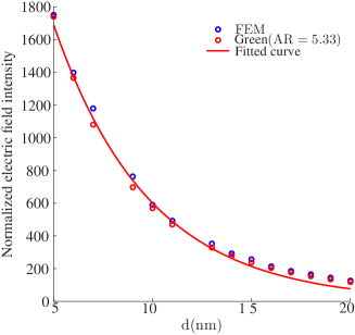
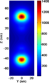
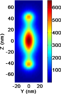
Figure 6 represents the near-field intensity calculated at for different meshing. We obtain a good agreement with the FEM-calculated map for the finest meshing (AR=1 and AR=2). Larger mesh aspect ratios are too rough to grasp the fast spatial field variation over the rod length. The agreement between the FEM and the GDT maps is not fully quantitative, even for the finest meshing (compare the maximum intensity in Figs. 2 and 6(a),6(b)). Since the optical response is extremelly sensitive to the exact object shape, we attribute this difference to the slight difference of the object shape due to the meshing. Indeed, GDT relies on a rectangular meshing so that we expect higher scattering on the edges. The corresponding object roughness is however of the order of so that the considered meshing is sufficient to describe object obtained within the state of the art of nanofabrication techniques. Considering a radius of 11 nm instead of 10 nm, we obtain a quantitative agreement between the FEM () and GDT () calculated intensities. We therefore conclude to the agreement between the two methods, within the nanofabrication tolerance.
4 LDOS
So far, we discussed the optical response of the metal nanorod to a plane wave excitation. This allows to detect the plasmon resonance and estimate the filed profile of the mode. However, LDOS map better describes the mode since it is an intrinsic properties of the system. The LDOS is also a key quantity to interprete electron energy loss spectroscopy (EELS) [39, 40] and governs the decay rate of a quantum emitter in confined system [41]. It can also be manipulated at the nanoscale, opening promising perspectives to realize original nano-optical devices [42].
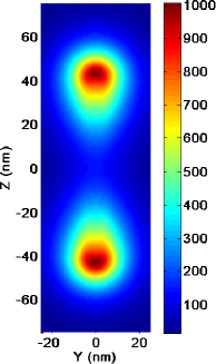
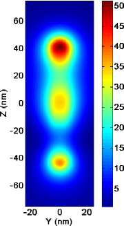
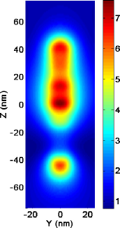
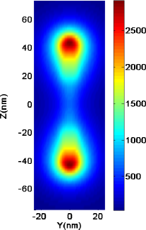
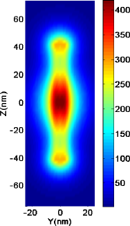
Figure 7 represents the LDOS calculated above the nanorod using Eq. 2 at the two resonances wavelength. As expected, the LDOS maps are symmetric and characterizes the suported modes, with a number of node in agreement with the Fabry-Perot resonator description [43]. The normalized LDOS amplitude of the first mode (up to ) is comparable to the normalized electric field intensity calculated for a plane wave excitation (Fig. 3(a), up to ). This again reveals the efficient excitation of this mode by a plane wave. On the contrary, the second mode is weakly excited by a plane wave, even at oblique incidence (compare the LDOS magnitude, up to in Fig. 7b and the electric intensity amplitudes, about ten times less in Figs. 6a and 7b).
5 Effect of the substrate
Finally, we discuss the effect of the substrate on the optical properties. This is an important point since plasmonic nanostructures are generally supported on a substrate. The presence of the substrate red shifts the resonance peak [44] so that it has to be taken into account. However, it could lead to difficult FEM numerical implementation since the field radiatively leaks into the substrate (most refringent medium) so that it has to be sufficiently discretized and requests important memory resources. On the opposite, GDT easily takes into account the presence of the substrate without increasing the memory cost and with a minor increase of the computing time. In the present case where the Green’s dyad has to be integrated over the mesh surface, it is advantageous to work within the dipole image (quasi-static) approximation that leads to an excellent agreement with the exact retarded description for nanostructures laying on a glass substrate [45]. Let us consider a dipole at position above a substrate of dielectric constant . The effect of the substrate on the dipole radiation is described by an image dipole at but in the homogeneous background of dielectric constant . If the observation point is above the substrate, the image dipole to consider writes . If the observation point is below the substrate, the image dipole to consider writes . Since the Green’s dyad expresses the field scattered by a dipolar source, the integrated formulation is easily deduced within the image dipole approximation. For instance,
| (14) |
for an observation point above the substrate.
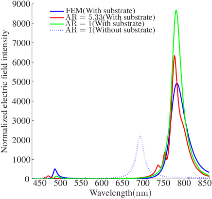
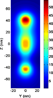
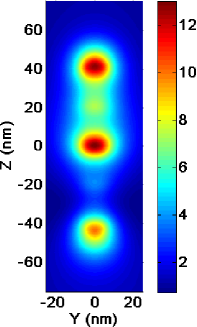
The near-field spectrum of the rod deposited on a glass substrate is calculated in figure 8 using GDT. We observe a strong shift of the resonances to the red. The resonance shift from to for the fundamental mode and to for the second order mode. The corresponding LDOS maps are represented in figure 9. We check that the mode profiles still correspond to the m=1 and m=2 SPP modes.
We also plot the near-field spectrum calculated using the FEM (Fig. 8). We observe good agreement with our GDT calculations except a lower intensity. We again attribute this to the extremelly sensitivity of the optical near-field response to the object shape. By considering a rod radius R=11 nm, FEM calculations lead to intensities comparable with GDT data. In addition, we would like to mention that the introduction of the PML layer is very critical for FEM in presence of the substrate. We observe strong variations of the calculated intensity with the PML center position. Best results are obtained when centering the PML at the rod (scatterer) center. If the PML is centered e.g. at the glass/air interface (that corresponds to a 10 nm shift only), the calculated intensity is divided by 2 (not shown). Therefore, comparison with the GDT allows to determine optimized PML parameters (size and position) for FEM before considering more complex shapes.
6 Conclusion
In summary we used a dyadic Green technique based on a cuboidal meshing to compute the electric near-field and the LDOS near a silver nanorod. The fast variations of the electric field in the metallic nanostructures are well described by a numerical integration of the Green’s tensor over elongated meshes. Moreover, the computing efforts are reduced by transforming the volume integration over a mesh to a surface integral. The efficiency and accuracy of this method are verified by comparing our results to those obtained by using finite element method. This is a confirmation of our technique, but reciprocically helps to determine the best parameters for FEM (notably PML). Green’s dyad technique presented in this paper is very convenient, especially in the case of elongated structure (with high aspect ratio). Moreover, since the meshing has to be increased at positions where the field fastly varies, this method could be advantageously combined with top-down extended meshing algorithms [46]. In addition, the presence of a substrate is easily taken into account, demonstrating the versatility and efficiency of the method. Since the method relies on an numerical integration of the Green’s dyad over a mesh surface, more complex meshing (e.g. tetrahedral) could also be considered, allowing for a better description of the object shapes. Finally, as soon as the Green’s tensor of the whole structure is calculated, every electromagnetic responses of the system are easily determined (electric and magnetic near and far field, LDOS, optical forces, EELS response, …).
7 Ackwnoledgements
O.D. acknowledges a stipend from the French program Investissement d’Avenir (LABEX ACTION ANR-11-LABX-01-01). The research leading to these results has received funding from the Agence Nationale de la Recherche (grants PLACORE ANR-13-BS10-0007 and HYNNA ANR-10-BLAN-1016 ) and the European Research Council under the European Community’s Seventh Framework Program FP7/2007-2013 (ERC SWIFT - Grant Agreement 306772). Calculations were performed using DSI-CCUB resources (Université de Bourgogne).
Bibliography
- [1] Agio, M. Optical antennas as nanoscale resonators. Nanoscale 4, 692–706 (2012).
- [2] Derom, S., Vincent, R., Bouhelier, A. & Colas des Francs, G. Resonance quality, radiative/ohmic losses and modal volume of Mie plasmons. EPL 98, 47008 (2012).
- [3] Bharadwaj, P., Deutsch, B. & Novotny, L. Optical antennas. Advances in Optics and Photonics 1, 438–483 (2009).
- [4] Olmon, R. L. & Raschke, M. B. Antenna-load interactions at optical frequencies: impedance matching to quantum systems. Nanotechnology 23, 444001 (2012).
- [5] Moskovits, M. Surface-enhanced spectroscopy. Reviews of Modern Physics 57, 783–826 (1985).
- [6] Pettinger, B. Single-molecule surface- and tip-enhanced raman spectroscopy. Molecular Physics 108, 2039–2059 (2010).
- [7] Girard, C. Near-field in nanostructures. Report on Progress in Physics 68, 1883–1933 (2005).
- [8] Pastoriza-Santos, I. & Liz-Marzan, L. M. Colloidal silver nanoplates. State of the art and future challenges. Journal of Materials Chemistry 18, 1713-1820 (2008).
- [9] Thete, A., Rojas, O., Neumeyer, D., Koetz, J. & Dujardin, E. Ionic liquid-assisted morphosynthesis of gold nanorods using polyethyleneimine-capped seeds. RSC Advances 3, 14294-14298 (2005).
- [10] Lakhtakia, A. Strong and weak forms of the method of moments and the coupled dipole method for scattering of time-harmonic electromagnetic fields. Journal of Modern Physics C 3, 583–603 (1992).
- [11] Paulus, M., Gay-Balmaz, P. & Martin, O. Green’s tensor technique for scattering in two-dimensional stratified media. Physical Review E 63, 66615 (2001).
- [12] Lévêque, G. et al. Polarization state of the optical near-field. Physical Review E 65, 36701 (2002).
- [13] Girard, C., Weeber, J. C., Dereux, A., Martin, O. J. F. & Goudonnet, J. P. Optical magnetic near–field intensities around nanometer–scale surface structures. Physical Review B 55, 16487–16497 (1997).
- [14] Novotny, L. Allowed and forbidden light in near-field optics. i. a single dipolar light source. Journal of the Optical Society of America 14, 91–104 (1997).
- [15] Colas des Francs, G., Girard, C., Weeber, J.-C. & Dereux, A. Relationship between scanning near-field optical images and local density of photonic states. Chemical Physics Letters 345, 512–516 (2001).
- [16] Girard, C., Martin, O., Lévêque, G., Colas des Francs, G. & Dereux, A. Generalized bloch equations for optical interactions in confined geometries. Chemical Physics Letters 404, 44 (2005).
- [17] Kottmann, J. P. & Martin, O. J. F. Accurate solution of the volume integral equation for high–permittivity scatterers. IEEE Transactions on Antennas and Propagation 48, 1719–1726 (2000).
- [18] Chaumet, P. C., Sentenac, A. & Rahmani, A. Coupled dipole method for scatterers with large permittivity. Physical Review E 70, 36606 (2004).
- [19] Gao, G., Torres-Verdín, C. & Habashy, T. Analytical techniques to evaluate the integrals of 3D and 2d spatial dyadic green’s functions. Progress In Electromagnetics Research, PIER 52, 47–80 (2005).
- [20] Myroshnychenko, V. et al, Modeling the Optical Response of Highly Faceted Metal Nanoparticles with a Fully 3D Boundary Element Method. Advanced Materials 20, 4288–4293 (2008).
- [21] Hohenester, U. & Trügler, A. Interaction of single molecules with metallic nanoparticles. IEEE Journal of Selected Topics in Quantum Electronics 14, 1430 (2008).
- [22] Kern, A. & Martin, O. Surface integral formulation for 3D simulations of plasmonic and high permittivity nanostructures. Journal of the Optical Society of America A 26, 732-740 (2009).
- [23] www.comsol.com
- [24] Colas des Francs, G. et al. Optical analogy to electronic quantum corrals. Physical Review Letters 86, 4950–4953 (2001).
- [25] Colas des Francs, G., Girard, C. & Dereux, A. Theory of near-field optical imaging with a single molecule as a light source. Journal of Chemical Physics 117, 4659–4666 (2002).
- [26] Yaghjian, A. Electric dyadic Green’s functions in the source region. Proceedings of the IEEE 68, 248–263 (1980).
- [27] Massa, E., Roschuk, T., Maier, S. & Giannini, V., Discrete-dipole approximation on a rectangular cuboidal point lattice: considering dynamic depolarization. Journal of the Optical Society of America A 1, 135-140 (2014).
- [28] Jin, J.-M. The Finite Element Method in Electromagnetics, Wiley IEEE Press, New York, (2002).
- [29] Berenger, J.-P., A Perfectly matched layer for the absorption of electromagnetic-waves. Journl of Computational Physics 114(2), 185-200 (1994).
- [30] Ould Agha, Y., Zolla, F., Nicolet, A., & Guenneau, S. On the use of PML for the computation of leaky modes: An application to microstructured optical fibres. COMPEL(The International Journal for Computation and Mathematics in Electrical and Electronic Engineering) 27(1), 95-109 (2008).
- [31] Nicolet, A., Zolla, F., Ould Agha, Y., & Guenneau, S. Geometrical transformations and equivalent materials in computational electromagnetism. COMPEL(The International Journal for Computation and Mathematics in Electrical and Electronic Engineering) 27(4), 806-819 (2008).
- [32] Johnson, P. & Christy, R. Optical constants of the noble metals. Physical Review B 6, 4370–4379 (1972).
- [33] Stout, B., Auger, J. C. & Devilez, A. Recursive T matrix algorithm for resonant multiple scattering: applications to localized plasmon excitations. Journal of the Optical Society of America A 25, 2549–2557 (2008).
- [34] Ditlbacher, H. et al. Silver nanowires as surface plasmon resonators. Physical Review Letters 95, 257403 (2005).
- [35] Novotny, L. Effective wavelength scaling for optical antennas. Physical Review Letters 98, 266802 (2007).
- [36] Cubukcu, E. & Capasso, F.. Optical nanorod antennas as dispersive one-dimensional fabry-pérot resonators for surface plasmons. Applied Physics Letters 95, 201101 (2009).
- [37] Lal, S., Grady, N. K., Goodrich, G. P. & Halas, N. J. Profiling the near field of a plasmonic nanoparticle with raman-based molecular rulers. Nano Letters 6, 2338–2343 (2006).
- [38] Deeb, C. et al. Quantitative analysis of localized surface plasmons based on molecular probing. ACS Nano 4, 4579–4586 (2010).
- [39] García de Abajo, F. & Kociak, M. Probing the photonic local density of states with electron energy loss spectroscopy. Physical Review Letters 100, 106804 (2008).
- [40] Bouhelier, A., Colas des Francs, G. & Grandidier, J. Plasmonics, From Basics to Advanced Topics, vol. 167 of Springer Series in Optical Sciences, chap. Surface plasmon imaging, 225–268 (Springer, 2012).
- [41] Barnes, W. Fluorescence near interfaces: the role of photonic mode density Journal of Modern Optics 45, 661-699 (1998).
- [42] Viarbitskaya, S. et al. Tailoring and imaging the plasmonic local density of states in crystalline nanoprisms. Nature Materials 12, 426–432 (2013).
- [43] Lim, J. et al. Imaging and dispersion relations of surface plasmon modes in silver nanorods by near-field spectroscopy. Chemical Physics Letters 1412, 41–45 (2005).
- [44] Weeber, J.-C., Girard, C., Dereux, A., Krenn, J. & Goudonnet, J. P. Near–field optical properties of localized plasmons around lithographically designed nanostructures. Journal of Applied Physics 86, 2576–2583 (1999).
- [45] Gay-Balmaz, P. & Martin, O. Validity of non-retarded Green’s tensor for electromagnetic scattering at surfaces. Optics Communications 184, 37–47 (2000).
- [46] Alegret, J., Käll,M. & Johansson, P. Top-down extended meshing algorithm and its applications to Green’s tensor nano-optics calculations. Physical Review E 75, 046702 (2007).