Nitride Multilayers as a Platform for Parallel
Two-Dimensional Electron-Hole Gases: MgO/ScN(111)
Abstract
At interfaces between insulating oxides LaAlO3 and SrTiO3, a two dimensional electron gas (2DEG) has been observed and well studied, while the predicted hole gas (2DHG) has not been realized due to the strong tendency of holes in oxygen orbitals to localize. Here we propose, via ab initio calculations, an unexplored class of materials for the realization of parallel two dimensional (2D), two carrier (electron+hole) gases: nitride-oxide heterostructures, with (111)-oriented ScN and MgO as the specific example. Beyond a critical thickness of five ScN layers, this interface hosts spatially separated conducting Sc- electrons and N- holes, each confined to two atomic layers – the transition metal nitride provides both gases. A guiding concept is that the N3- anion should promote robust two carrier 2D hole conduction compared to that of O2-; metal mononitrides are mostly metallic and even superconducting while most metal monoxides are insulating. A second positive factor is that the density of transition metal ions, hence of a resulting 2DG, is about three times larger for a rocksalt (111) interface than for a perovskite(001) interface. Our results, including calculation of Hall coefficient and thermopower for each conducting layer separately, provide guidance for new exploration, both experimental and theoretical, on nitride-based conducting gases that should promote study of long sought exotic states viz. new excitonic phases and distinct, nanoscale parallel superconducting nanolayers.
pacs:
73.20.-r, 71.30.+h, 31.15.A-I background
The unexpected magnetic and electronic phases appearing at the interface between two perovskite oxides have been studied extensively during the last decade.Ohtomo and Hwang (2004); Thiel et al. (2006); Caviglia et al. (2010); Brinkman et al. (2007); Reyren et al. (2007) The discovery of a two dimensional electron gas (2DEG) at the interface between LaAlO3/ SrTiO3(LAO/STO) by Ohtomo and HwangOhtomo and Hwang (2004) stimulated excitement for the design of similar heterostructures and their possible use in electronic devices.Mannhart and Schlom (2010); Park et al. (2009) The further realization that electronic reconstruction could provide a parallel, nanoscale 2DEG and 2D hole gas (2DHG) provided a more exotic vista,Pentcheva et al. (2010); Huijben et al. (2012) including two band, two carrier magnetic or superconducting systems, as well as long sought excitonic condensates.Millis and Schlom (2010); Eisenstein and MacDonald (2004) Substantial theorizing has been waiting favorable experimental platforms for progress. Unfortunately, at oxide interfaces the hole gas has never materialized. Due to the proclivity of holes to occupy O orbitals, the -type interface is always observed to be non-conducting, eliminating the many possibilities provided by two, or many, 2DEGs and 2DHGs separated by only 2-3 nm.Chen et al. (2010); Hotta et al. (2007)
The difficulty in obtaining conducting -type interfaces in oxides suggests using related but less electronegative ions, bringing to mind nitrides. Whereas transition metal monoxides are mostly strongly correlated (Mott) insulators, Rivadulla et al. (2007) the existing mononitrides are usually conducting and even superconducting.Matthias and Hulm (1952); Matthias et al. (1963) This tendency toward conductivity while forming similar or even identical structures brings a new dimension to the design of heterostructures of insulators having active interfaces.
(001) layers of transition metal mononitrides (or monoxides) with rocksalt structure are charge neutral, thus being ineffective in providing the 2D gases of interest here. This layer neutrality, and the challenges provided by localized O states, invites innovative material design, especially because layer-by-layer growth provides the experimental capability of concerted theory plus experiment design of novel materials with tailored properties at the nanoscale.
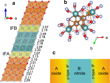
The simplest polar structure in rocksalt mononitrides is provided by (111) orientation, where oppositely charged metal and anion-atom layers alternately stack along the [111] direction (see Fig. 1). In spite of the widely discussed instability of ideal polar surfaces in a semi-infinite geometry, MgO films with atomically flat (111) surface regions have been reported using layer-by-layer growth on a variety of substrates.Arita et al. (2004); Goniakowski et al. (2004, 2007); Craft et al. (2006); Goodrich et al. (2007); Posadas et al. (2008); Susaki et al. (2009); Matsuzaki et al. (2010, 2011) These atomically flat surfaces are promising to explore the possibility of polar interface engineering using simple metal monoxides and mononitrides with rocksalt structure.
Here, we explore the use of the narrow gap semiconductor ScN,Smith et al. (2001); Lambrecht (2000); Jiang et al. (2010) sandwiched between highly insulating MgORoessler and Walker (1967); Kenmochi et al. (2004) spacer layers, as a material to support bilayer electron+hole conducting gases and all the unusual phases that have been anticipated in such heterostructures. By means of first principles calculations, we have designed and explored MgO/ScN(111) superlattices with varying ScN thickness containing two charge imbalanced interfaces: one -type and one -type. Beyond a ScN thickness threshold of five layers these interfaces host conducting electron+hole gases, both gases lying within but on opposite edges of the ScN layer. Use of the N anion should promote robust two carrier 2D conduction compared to oxides, where holes are prone to localization. ScN is a propitious choice of nitride, since it has been shown that it can be hole-doped in bulk to a similar magnitude of conductivity as natively electron-doped samples.Saha et al. (2013)
II Computational Methods
Our electronic structure calculations were performed within density functional theory Hohenberg and Kohn (1964); Jones and Gunnarsson (1989) using the all-electron, full potential code wien2k Schwarz and Blaha (2003) based on the augmented plane wave plus local orbitals (APW+lo) basis set.Sjöstedt et al. (2000)
All calculations were well converged with respect to all the parameters used. In particular, we used RMTKmax= 7.0 (the product of the smallest of the atomic sphere radius RMT and the plane wave cutoff parameter Kmax), which determines the size of the basis set. The chosen RMT are 1.95 a.u. for Sc, 1.73 a.u. for N, 1.79 a.u. for Mg and 1.69 a.u. for O. The calculations used a 43435 -mesh for the integrations over the Brillouin zone. For the structural relaxations we have used the Wu-Cohen (WC) version of the generalized gradient approximation (GGA)Wu and Cohen (2006) that gives better lattice parameters for MgO than the Perdew-Burke-Ernzerhof version (PBE).Perdew et al. (1996); Tran et al. (2007) The optimized lattice parameters derived within GGA-WC for MgO and ScN are 4.23 and 4.50 Å, respectively.
An accurate ab initio description requires a method able to reproduce the band gap of the individual components as well as their band alignment at the interface, both of which are generally beyond the capabilities of GGA or local density approximation (LDA). To be able to reproduce the bulk gap of ScN, we have used the semilocal potential developed by Tran and Blaha based on a modification of the Becke-Johnson potential (TB-mBJ).Tran and Blaha (2009); Koller et al. (2011) This is a local approximation (local in the density and the kinetic energy density) to an atomic exact-exchange potential and a screening term + GGA correlation that allows the calculation of band gaps with an accuracy similar to the much more expensive GW or hybrid methods.Tran and Blaha (2009); Koller et al. (2011) The TB-mBJ functional is a potential-only functional, i.e., there is no corresponding TB-mBJ exchange-correlation energy functional. In this respect it is applied as a self-energy correction, and one based on improved intra-atomic exchange processes. The band structure for bulk ScN obtained within TB-mBJ reproduces the experimental band gap and is shown in the Appendix.
Based on the agreement with the experiments for ScN bulk, TB-mBJ was the scheme applied to the ScN/MgO (111) multilayers. We have modeled MgO/ScN(111) multilayers which are 2- to 7-ScN layers thick. A barrier of 3-4 MgO layers (about 1.5 nm thick) between ScN blocks has been used for all the calculations, checking that it is sufficient to guarantee the lack of interaction between ScN blocks. The multilayers are modeled with the in-plane lattice parameters constrained to those of MgO (fixed to the value 4.23 Å, obtained by optimizing the cell volume within WC-GGA).
For all the multilayers we performed calculations with fully relaxed atomic positions also optimizing the value of the -lattice parameter (off-plane), i.e. allowing atomic displacements along the -axis and thus relaxing the inter-plane distances for the structures with different number of ScN layers. The optimized values of the -lattice parameter result in a slight increase from the value obtained by constructing the multilayers from the MgO bulk unit cell, of about 1% to 2% for multilayers two to seven ScN layers thick. This is expected, as the in-plane lattice parameter inside the ScN blocks is constrained to the smaller value of MgO. The average distances between layers along the c axis are shown in Fig. 1 for a multilayer 5 ScN-layers thick. The main feature in the calculated relaxed geometry consisting in one shorter and one longer Sc/Mg-N/O bond length along c can be observed.
III Analysis of Results
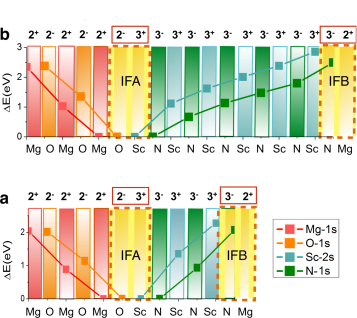
The underlying structure of the multilayers is shown in Fig. 1. When growing periodically arranged superlattices two polar interfaces arise: the so-called interface A (IFA, -type) (2-/3+) and interface B (IFB, -type) (3-/2+). If the system remains insulating (which is not obvious a priori since ScN is a small gap semiconductor) the polar discontinuity will produce a large electrostatic potential offset between the two interfaces, resulting in potential gradient reflecting the internal electric field. This effect can be tracked most directly by following the layer-by-layer core level eigenvalues. These eigenvalues are shown in Fig. 2 for multilayers with different ScN thickness. For thin ScN layers a potential difference of 2 to 3 eV on each block of the multilayer develops. This gradient corresponds to a local electric field of 1.1107 V/cm acting across the interface region, on the order of that obtained in LAO/STO heterostructures.Bogorin et al. (2010); Pentcheva et al. (2010) The layer-by-layer shifts in the core levels are about 1 eV in the thinner multilayer and are reduced when the interfaces metalize. Superlattice periodicity forces the potential to return to zero after it has ramped up the ScN slab.
As a consequence of this potential gradient (that scales with thickness) there is an insulator-to-metal transition as the number of ScN layers is increased. For multilayers 3 ScN layers thick the gap (1.5 eV) is widened by confinement with respect to the value in the bulk (see this band structure in the Appendix), for 4 ScN layers the gap is reduced to 0.34 eV, and from a critical thickness of 5 ScN layers the band structures are metallic. Insulator-to-metal transitions with thickness have been observed in a number of oxide-based heterostructures in the literature, both polar and non-polar, including open-shell and closed-shell materials, such as multilayers of VO2/TiO2,Pardo and Pickett (2010a) SrVO3/SrTiO3,Kim et al. (2000); Pardo and Pickett (2010b); Yoshimatsu et al. (2010) LaVO3/SrTiO3, Assmann et al. (2013) and the above mentioned LaAlO3/SrTiO3.Thiel et al. (2006); Bogorin et al. (2010)
III.1 Electronic structure
The Sc and N projected density of states (DOS) for three and six ScN layers are shown in Fig. 3 where the the insulator-to-metal transition with thickness is evident. The nearly rigid upward shift consistent with the above described potential gradient can be seen by focusing on the N- bands (orange) that move towards the Fermi level from IFA to IFB. The insulating state obtained for thinner ScN layers is shown in Fig. 3(a). The gap is formed between occupied N- states and unoccupied Sc- states.
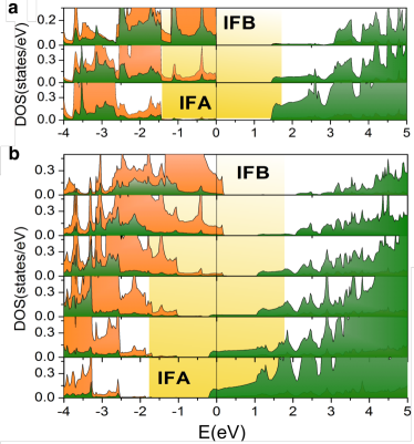
For multilayers with a thicker ScN block both interfaces host metallic states as shown in Fig. 3(b). N- and Sc- bands overlap in energy at IFB and IFA, respectively, leading to spatially separated hole and electron conducting states. The band structure and Fermi surface plots (shown in the Appendix) indicate that the nearly circular hole pocket is centered at whereas the nearly circular electron pocket is centered at the hexagonal zone face point. This band overlap provides a multilayer realization of the polar discontinuity scenario of electronic reconstruction, originally found for LAO overlayers on an STO substrate.Pentcheva and Pickett (2009); Nakagawa et al. (2006) Upon metallization electrons are transferred from one interface of the unit cell to the other, thus reducing the internal field although a substantial gradient persists (of the order of 107 V/cm). The result is two bilayer conductors each confined to two atomic layers (IF and IF-1), constituting a periodic array of alternating electron and hole 2DGs. The N-derived 2DHG should promote robust two carrier 2D conduction instead of insulating -type interfaces.
Using a transition metal nitride provides yet other opportunities. The superconductivity observed in many samples of STO/LAO may be simply the state observed in -doped STO (confined somewhat to reflect a 2D superconducting behavior), or it might be a new phenomenon due to an interfacial pairing process. Ti, Zr, V, and Nb mononitrides with a rocksalt structure were among the first discovered superconductors with ’s up to 16 K.Matthias and Hulm (1952); Matthias et al. (1963) Also, electron-doped transition metal chloronitrides MNCl (M = Hf, Zr, Ti) are superconducting in the 15-26 K range,Kasahara et al. (2015) putting them among the top classes of high temperature superconductors. The observation of superconductivity at a transition metal nitride interface (as in this ScN/MgO system) is an exciting possibility, and if discovered would support that superconductivity observed at STO/LAO interfaces is derivative of bulk STO superconductivity.
Excitons (electron-hole bound states) are a topic of great importance in condensed matter physics and play a central role in solar energy conversion.Millis and Schlom (2010); Eisenstein and MacDonald (2004); Gregg (2003); Assmann et al. (2013) For four and fewer ScN layers a small gap remains, providing the platform for formation of excitons that are indirect in -space and whose components are separated in real space, giving the possibility of long-lived excitons. Bristowe et al. Bristowe et al. (2009) noted the possibility of exciton formation in the context of LaAlO3/SrTiO3 multilayers with alternating and interfaces, stymied because hole conduction is very difficult to achieve. In LAO/STO (001) overlayers a parallel electron-hole conduction has been reported only when an STO capping layer is added to protect the uppermost 2DEG.Pentcheva et al. (2010); Huijben et al. (2012) The hole conduction relies on a surface state whereas the 2DEG is in the interfacial layer. The reported hole mobility is low and it is expected that the holes can become localized or eliminated in uncapped STO/LAO systems more strongly. The route proposed here for the formation of proximal electron and hole gases should provide the desired platform as compared to the standard LAO/STO heterostructure.
In addition to the more robust hole conduction, here the system is much simpler (1/3 fewer chemical species need be introduced in the standard chambers used for thin film epitaxial growth) and that should be an advantage in terms of growth. Importantly, the problem with oxygen vacancies in STO (due to the Ti valence flexibility) is absent in MgO.
III.2 Bilayer transport
To allow for additional experimental tests of the origin and nature of the conduction mechanism in these multilayers, we have calculated the temperature dependence of the thermopower . The expression for (diagonal) within Bloch-Boltzmann transport theoryAllen et al. (1988) is
| (1) |
| (2) |
in terms of the energy-dependent conductivity , where is the Boltzmann constant, is the fundamental charge, the density of states, the group velocity, the distribution function, and the scattering time. The energy dependence of depends on the scattering mechanism and is usually treated as unimportant on a fine energy scale, as we do here. For low temperature, the magnitude and sign of Sαα depend only on the energy derivative of at where is the chemical potential.
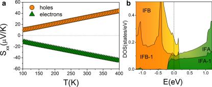
One should note that the calculation of the desired thermopower coefficient requires modification of existing methods. The band structure shown in Fig. 6 is like that of a compensated semimetal, with a few electron carriers and compensating hole carriers and Fermi energies (occupied bandwidths) of 100-200 meV. In a conventional semimetal the carriers permeate the entire cell and make compensating contributions to the net value. However, in the current structure the 2D gases are distinct and it is their individual thermopowers that are of interest. The contributions must be calculated separately, as we have done, using the Bloch-Boltzmann expressions Allen et al. (1988), which involve only near Fermi surface quantities versus those from throughout the occupied bands (such as the carrier density) and takes into account the band nonparabolicity that occurs in this system. The results are presented in Fig. 4. Values of the thermoelectric power for electrons and holes are linear with T and virtually identical in size ( = 0.11V/K2). Fig. 4(b) shows the density of states (DOS) of electron and hole bands separately. The differences in near = 0 are evident, with the hole DOS in particular having a non-2D like behavior.
The thermopower obtained in this ScN/MgO(111) multilayer is different than some behaviors discussed elsewhere.Filippetti et al. (2012) 2DEGs can be obtained in related interfaces but involving only one type of carrier.Ohta et al. (2007) Quantum confinement, which narrows (some) bands, may produce a thermopower enhancement.Hicks and Dresselhaus (1993); Sofo and Mahan (1994) Interestingly, ScN itself has been found to yield an anomalously large thermopower albeit at high doping level,Kerdsongpanya et al. (2011); Zebarjadi et al. (2009); Burmistrova et al. (2013) suggested to result from localized im- purity states close to the Fermi level.Kerdsongpanya et al. (2012a) The thermopowers of the individual 2DGs of this heterostructure represent an advance beyond previous theoretical or experimental studies separating the 2DEG and 2DHG contributions.
Doped semiconductors, which is what each interface 2DG is, typically display large thermopowers, and though still hotly pursued, large thermopowers are not always what an application requires. This result of nearly exactly canceling electron and hole thermopowers provides the opportunity of engineering small to negligible electrothermal conversion, which may be needed in some applications, as opposed to the more visible energy conversion between electrical energy and heat. Currents that do not drag along net heat should have applications in electronics, such as providing cooling to offset Joule heating. All thermopower measurements have to be corrected by adding the absolute thermopower of the lead wires. Materials with negligible thermopower should allow the thermopower of other substances to be determined directly.Yoo et al. (2000a)
As for the thermopower, the Hall coefficient of the separate 2DGs requires modification of existing methods. Recall that the Hall coefficient is a Fermi surface property, obtained from first and second derivatives of the band dispersion on the Fermi surface. Only for quadratic, single band systems can be related to a carrier density obtained from the integrated density of states. More specifically, if in the definition = the current from both electron and hole 2DGs is used, the result incorporates quantities from two separate subsystems, whereas we want for each conducting layer separately. The calculated Hall coefficient for electron and hole-like bands separately gives = 0.11 m3/C, = -0.16 m3/C, both T-independent above 200 K. These values correspond in a standard (but simplistic, see below) interpretation to an effective carrier density = 3carriers/cm2 and = 4carriers/cm2. These “Hall densities” need not be equal, because the bands are not precisely parabolic as is assumed when is converted to carrier density.
Measured values of Hall density of oxide-only interfaces are similar to our calculated values just above, so it is worthwhile to look more carefully at the numbers. The values for LAO/STO(001) led to considerable discussion because the polar mismatch picture implies that for thick layers (i.e. isolated interfaces) the transferred density should be 0.5 carrier per interface cell, which is almost an order of magnitude larger.Caviglia et al. (2010); Pentcheva et al. (2010) Of course, for thin ScN layers as here as for most LAO/STO calculations, just beyond the polar mismatch insulator-to-metal transition, only enough electrons transfer across the layer, thereby counteracting the internal field enough to line up the 2DEG Fermi level with the 2DHG Fermi level.
The actual transferred charge density , from the integrated DOS, is 0.09 per interface cell, or 1.11014/cm2, transferred from the two nearly degenerate -centered hole bands to the two symmetry-related, -centered electron bands. This factor of three difference can be reconciled by noting that the behavior of at the Fermi level (Fig. 4) is not typical of quadratic bands (i.e. which would be constant) and that is sensitive to the first and second derivatives of on the Fermi surfaces. The numbers also highlight a difference of this ScN/MgO(111) system compared to LAO/STO(001): the areal density of transition metal ions is nearly three times larger, with neighbors in the rocksalt (111) plane being and close-packed, versus in perovskite (001) the separation is and not close-packed. The lattice constants do not differ greatly. Thus rocksalt (111) interfaces offer the possibility of much higher densities as well as 2DHGs that actually conduct.
IV summary
We have proposed a novel approach to achieve two dimensional, two carrier bilayer conducting systems by moving away from oxygen for hole conduction. Designing by choice of anion and by orientation of the interface, and studying with first principles calculations, hybrid oxide-nitride multilayers are proposed as a platform for the realization of parallel two dimensional, two carrier (electron+hole) gases. The basic concept builds on a slab of a narrow gap transition metal nitride (B) sandwiched between a wide gap insulating oxide (A). The polar discontinuities at the A and B interfaces provide an internal electric field that raises the N- valence band maximum above the Sc- conduction band minimum, with resulting charge transfer metalizing both interfaces. The use of the narrow gap nitride ScN means that both signs of carriers live in ScN. Electrically MgO is inert, shifting the active component from an oxide to a nitride.
Acknowledgements.
V. P. thanks MINECO for project MAT2013-44673-R, the Xunta de Galicia through project EM2013/037, and Spanish Government for financial support through the Ramón y Cajal Program. W.E.P. acknowledges many conversations with R. Pentcheva on the theory and phenomenology of oxide interfaces and multilayers. A.S.B. and W.E.P were supported by Department of Energy Grant No. DE-FG02-04ER46111.V appendix
V.1 Electronic structure of bulk ScN
ScN is a nonmagnetic semiconducting transition metal mononitride with a band gap of 0.9 eV that has remarkable physical properties such as high chemical stability, high melting point (2600C), and large mechanical hardness (H= 21 GPa).Smith et al. (2001)
A number of first principles calculations have been performed on ScN. Early density functional theory-based calculations employing the LDA Monnier et al. (1985) or XNeckel et al. (1976); Eibler et al. (1983) approximations predicted ScN to be a semimetal. Exact exchange and screened exchange calculations confirm that ScN is a semiconductor with an indirect - band gap, consistent with experiments. However, the calculated band gap of 1.6 eV is significantly larger than the experimental value of 0.9 eV.Gall et al. (2001) The LDA+ULiechtenstein et al. (1995) scheme improves over GGA or LDA in the study of systems containing correlated electrons by introducing the on-site Coulomb repulsion applied to localized electrons (in this case Sc- states). For ScN, LDA/GGA+ calculations using a value as high as 6 eV are only able to open an indirect gap of 0.40 to 0.55 eV, respectively, far from the one determined experimentally.Abu-Jafar et al. (2010) LDA calculations complemented with estimated quasiparticle corrections and calculations of the optical response give an indirect band gap of 0.9 eV with a first direct gap at of 2 eV.Lambrecht (2000) Quasiparticle G0W0 calculations predict ScN to have an indirect band gap between - of 0.99 eV.Qteish et al. (2006) Also hybrid functionals show the opening of a band gap of 0.9 eV.Kerdsongpanya et al. (2012b)
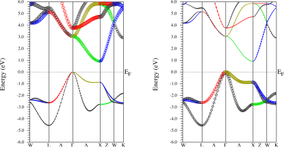
Figure 5 shows the band structure with band character plot (N and Sc character highlighted) for ScN obtained within TB-mBJ. The band gap is formed between occupied N- and unoccupied Sc- states and the experimental value of the gap is reproduced: an indirect band gap of 1.0 eV between - is obtained as well as the direct gap of 2.1 eV at . Thus TB-mBJ provides a computationally efficient method of producing and accurate band structure, and it has been applied for the results discussed in this manuscript.
V.2 Electronic structure of MgO/ScN(111) multilayers
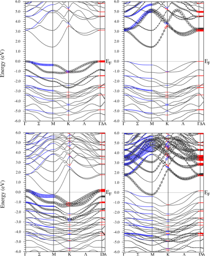
Figure 6 shows the band structures with band character plot that complement Fig. 3 in the main text, which shows the corresponding DOS. The bands crossing the Fermi level are indeed N- at IFB and Sc- at the IFA.
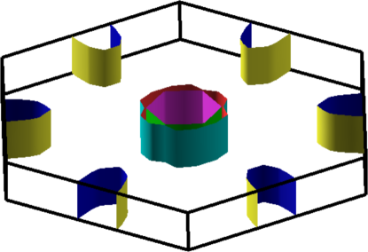
Figure 7 shows that these bands give rise to nearly circular Fermi surfaces coming from the electron (centered at ) and hole pockets (centered at ) respectively, as discussed in the main text.
References
- Ohtomo and Hwang (2004) A. Ohtomo and H. Hwang, Nature 427, 423 (2004).
- Thiel et al. (2006) S. Thiel, G. Hammerl, A. Schmehl, C. W. Schneider, and J. Mannhart, Science 313, 1942 (2006).
- Caviglia et al. (2010) A. D. Caviglia, S. Gariglio, C. Cancellieri, B. Sacépé, A. Fête, N. Reyren, M. Gabay, A. F. Morpurgo, and J.-M. Triscone, Phys. Rev. Lett. 105, 236802 (2010).
- Brinkman et al. (2007) A. Brinkman, M. Huijben, M. van Zalk, J. Huijben, U. Zeitler, J. C. Maan, W. G. van der Wiel, G. Rijnders, D. H. A. Blank, and H. Hilgenkamp, Nat. Mater. 6, 493 (2007).
- Reyren et al. (2007) N. Reyren, S. Thiel, A. D. Caviglia, L. F. Kourkoutis, G. Hammerl, C. Richter, C. W. Schneider, T. Kopp, A.-S. R etschi, D. Jaccard, et al., Science 317, 1196 (2007).
- Mannhart and Schlom (2010) J. Mannhart and D. G. Schlom, Science 327, 1607 (2010).
- Park et al. (2009) S. Park, D. H. Lee, J. Xu, B. Kim, S. W. Hong, U. Jeong, T. Xu, and T. P. Russell, Science 323, 030 (2009).
- Pentcheva et al. (2010) R. Pentcheva, M. Huijben, K. Otte, W. E. Pickett, J. E. Kleibeuker, J. Huijben, H. Boschker, D. Kockmann, W. Siemons, G. Koster, et al., Phys. Rev. Lett. 104, 166804 (2010).
- Huijben et al. (2012) M. Huijben, D. Kockmann, J. Huijben, J. E. Kleibeuker, A. van Houselt, G. Koster, D. H. A. Blank, H. Hilgenkamp, G. Rijnders, A. Brinkman, et al., Phys. Rev. B 86, 035140 (2012).
- Millis and Schlom (2010) A. J. Millis and D. G. Schlom, Phys. Rev. B 82, 073101 (2010).
- Eisenstein and MacDonald (2004) J. P. Eisenstein and A. H. MacDonald, Nature 432, 691 (2004).
- Chen et al. (2010) H. Chen, A. Kolpak, and S. Ismail-Beigi, Phys. Rev. B 82, 085430 (2010).
- Hotta et al. (2007) Y. Hotta, T. Susaki, and H. Y. Hwang, Phys. Rev. Lett. 99, 236805 (2007).
- Rivadulla et al. (2007) F. Rivadulla, J. Fernández-Rossier, M. García-Hernández, M. A. López-Quintela, J. Rivas, and J. B. Goodenough, Phys. Rev. B 76, 205110 (2007).
- Matthias and Hulm (1952) B. T. Matthias and J. K. Hulm, Phys. Rev. 87, 799 (1952).
- Matthias et al. (1963) B. T. Matthias, T. H. Geballe, and V. B. Compton, Rev. Mod. Phys. 35, 1 (1963).
- Arita et al. (2004) R. Arita, Y. Tanida, S. Entani, M. Kiguchi, K. Saiki, and H. Aoki, Phys. Rev. B 69, 235423 (2004).
- Goniakowski et al. (2004) J. Goniakowski, C. Noguera, and L. Giordano, Phys. Rev. Lett. 93, 215702 (2004).
- Goniakowski et al. (2007) J. Goniakowski, C. Noguera, and L. Giordano, Phys. Rev. Lett. 98, 205701 (2007).
- Craft et al. (2006) H. S. Craft, J. F. Ihlefeld, M. D. Losego, R. Collazo, Z. Sitar, and J.-P. Maria, Appl. Phys. Lett 88, 212906 (2006).
- Goodrich et al. (2007) T. L. Goodrich, J. Parisi, Z. Cai, and K. S. Ziemer, Appl. Phys. Lett 90, 042910 (2007).
- Posadas et al. (2008) A. Posadas, F. J. Walker, C. H. Ahn, T. L. Goodrich, Z. Cai, and K. S. Ziemer, Appl. Phys. Lett 92, 233511 (2008).
- Susaki et al. (2009) T. Susaki, S. Kumada, T. Katase, K. Matsuzaki, M. Miyakawa, and H. Hosono, Applied Physics Express 2, 091403 (2009).
- Matsuzaki et al. (2010) K. Matsuzaki, H. Hosono, and T. Susaki, Phys. Rev. B 82, 033408 (2010).
- Matsuzaki et al. (2011) K. Matsuzaki, H. Takagi, H. Hosono, and T. Susaki, Phys. Rev. B 84, 235448 (2011).
- Smith et al. (2001) A. R. Smith, H. A. H. AL-Brithen, D. C. Ingram, and D. Gall, J. Appl. Phys. 90, 1809 (2001).
- Lambrecht (2000) W. R. L. Lambrecht, Phys. Rev. B 62, 13538 (2000).
- Jiang et al. (2010) H. Jiang, R. I. Gomez-Abal, P. Rinke, and M. Scheffler, Phys. Rev. B 82, 045108 (2010).
- Roessler and Walker (1967) D. M. Roessler and W. C. Walker, Phys. Rev. 159, 733 (1967).
- Kenmochi et al. (2004) K. Kenmochi, V. A. Dinh, K. Sato, A. Yanase, and H. Katayama-Yoshida, Journal of the Physical Society of Japan 73, 2952 (2004).
- Saha et al. (2013) B. Saha, G. Naik, V. P. Drachev, A. Boltasseva, E. E. Marinero, and T. D. Sands, J. Appl. Phys. 114, 063519 (2013).
- Hohenberg and Kohn (1964) P. Hohenberg and W. Kohn, Phys. Rev. 136, B864 (1964).
- Jones and Gunnarsson (1989) R. O. Jones and O. Gunnarsson, Rev. Mod. Phys. 61, 689 (1989).
- Schwarz and Blaha (2003) K. Schwarz and P. Blaha, Comp. Mater. Sci. 28, 259 (2003), ISSN 0927-0256, proceedings of the Symposium on Software Development for Process and Materials Design.
- Sjöstedt et al. (2000) E. Sjöstedt, L. Nördstrom, and D. Singh, Solid State Communications 114, 15 (2000), ISSN 0038-1098.
- Wu and Cohen (2006) Z. Wu and R. E. Cohen, Phys. Rev. B 73, 235116 (2006).
- Perdew et al. (1996) J. P. Perdew, K. Burke, and M. Ernzerhof, Phys. Rev. Lett. 77, 3865 (1996).
- Tran et al. (2007) F. Tran, R. Laskowski, P. Blaha, and K. Schwarz, Phys. Rev. B 75, 115131 (2007).
- Tran and Blaha (2009) F. Tran and P. Blaha, Phys. Rev. Lett. 102, 226401 (2009).
- Koller et al. (2011) D. Koller, F. Tran, and P. Blaha, Phys. Rev. B 83, 195134 (2011).
- Bogorin et al. (2010) D. F. Bogorin, C. W. Bark, H. W. Jang, C. Cen, C. M. Folkman, C.-B. Eom, and J. Levy, Appl. Phys. Lett 97, 013102 (2010).
- Pardo and Pickett (2010a) V. Pardo and W. E. Pickett, Phys. Rev. B 81, 035111 (2010a).
- Kim et al. (2000) D. Kim, D.-W. Kim, B. Kang, T. Noh, D. Lee, K.-B. Lee, and S. Lee, Solid State Communications 114, 473 (2000), ISSN 0038-1098.
- Pardo and Pickett (2010b) V. Pardo and W. E. Pickett, Phys. Rev. B 81, 245117 (2010b).
- Yoshimatsu et al. (2010) K. Yoshimatsu, T. Okabe, H. Kumigashira, S. Okamoto, S. Aizaki, A. Fujimori, and M. Oshima, Phys. Rev. Lett. 104, 147601 (2010).
- Assmann et al. (2013) E. Assmann, P. Blaha, R. Laskowski, K. Held, S. Okamoto, and G. Sangiovanni, Phys. Rev. Lett. 110, 078701 (2013).
- Pentcheva and Pickett (2009) R. Pentcheva and W. E. Pickett, Phys. Rev. Lett. 102, 107602 (2009).
- Nakagawa et al. (2006) N. Nakagawa, H. Y. Hwang, and D. A. Muller, Nat. Mater 5, 204 (2006).
- Kasahara et al. (2015) Y. Kasahara, K. Kuroki, S. Yamanaka, and Y. Taguchi, Physica C, in press arxiv 1412.4447 (2015).
- Gregg (2003) B. A. Gregg, J. Phys. Chem. B 107, 4688 (2003).
- Bristowe et al. (2009) N. C. Bristowe, E. Artacho, and P. B. Littlewood, Phys. Rev. B 80, 045425 (2009).
- Allen et al. (1988) P. B. Allen, W. E. Pickett, and H. Krakauer, Phys. Rev. B 37, 7482 (1988).
- Filippetti et al. (2012) A. Filippetti, P. Delugas, M. J. Verstraete, I. Pallecchi, A. Gadaleta, D. Marré, D. F. Li, S. Gariglio, and V. Fiorentini, Phys. Rev. B 86, 195301 (2012).
- Ohta et al. (2007) H. Ohta, S. Kim, Y. Mune, T. Mizoguchi, K. Nomura, S. Ohta, T. Nomura, Y. Nakanishi, Y. Ikuhara, M. Hirano, et al., Nat. Mater 6, 129 (2007).
- Hicks and Dresselhaus (1993) L. D. Hicks and M. S. Dresselhaus, Phys. Rev. B 47, 12727 (1993).
- Sofo and Mahan (1994) J. O. Sofo and G. D. Mahan, Appl. Phys. Lett 65, 2690 (1994).
- Kerdsongpanya et al. (2011) S. Kerdsongpanya, N. Van Nong, N. Pryds, A. Žukauskaitė, J. Jensen, J. Birch, J. Lu, L. Hultman, G. Wingqvist, and P. Eklund, Appl. Phys. Lett 99, 232113 (2011).
- Zebarjadi et al. (2009) M. Zebarjadi, Z. Bian, R. Singh, A. Shakouri, R. Wortman, V. Rawat, and T. Sands, J. Electron. Mater. 38, 960 (2009).
- Burmistrova et al. (2013) P. V. Burmistrova, J. Maassen, T. Favaloro, B. Saha, S. Salamat, Y. Rui Koh, M. S. Lundstrom, A. Shakouri, and T. D. Sands, J. Appl. Phys. 113, 153704 (2013).
- Kerdsongpanya et al. (2012a) S. Kerdsongpanya, B. Alling, and P. Eklund, Phys. Rev. B 86, 195140 (2012a).
- Yoo et al. (2000a) H. -I. Yoo, M. W. Barsoum, and T. El-Raghy, Nature 407, 581 (2000).
- Monnier et al. (1985) R. Monnier, J. Rhyner, T. M. Rice, and D. D. Koelling, Phys. Rev. B 31, 5554 (1985).
- Neckel et al. (1976) P. Neckel, R. Rastl, P. Eibler, P. Weinberger, and K. Schwarz, J. Phys. C 9, 579 (1976).
- Eibler et al. (1983) R. Eibler, M. Dorrer, and A. Neckel, Theor. Chim. Acta 63, 133 (1983).
- Gall et al. (2001) D. Gall, M. Stadele, K. Jarrendahl, I. Petrov, P. Desjardins, R. T. Haasch, T.-Y. Lee, and J. E. Greene, Phys. Rev. B 63, 125119 (2001).
- Liechtenstein et al. (1995) A. I. Liechtenstein, V. I. Anisimov, and J. Zaanen, Phys. Rev. B 52, R5467 (1995).
- Abu-Jafar et al. (2010) M. Abu-Jafar, A. Abu-Labdeh, and M. El-Hasan, Comp. Mater. Sci. 50, 269 (2010), ISSN 0927-0256.
- Qteish et al. (2006) A. Qteish, P. Rinke, M. Scheffler, and J. Neugebauer, Phys. Rev. B 74, 245208 (2006).
- Kerdsongpanya et al. (2012b) S. Kerdsongpanya, B. Alling, and P. Eklund, Phys. Rev. B 86, 195140 (2012b).