Generation of fully spin-polarized currents in three-terminal graphene-based transistors
Abstract
We propose three-terminal spin devices with graphene nanoribbons (terminals) and a graphene flake (channel) to generate a highly spin-polarized current without an external magnetic field or ferromagnetic electrodes. The Hubbard repulsion within the mean-field approximation plays the main role to separate the unpolarized electric current at the source terminal into spin-polarized currents at the drain terminals. It is shown that by modulating one of the drain voltages, a fully spin-polarized current can be generated in the other drain terminal. In addition, the geometry of the channel and the arrangement of edge atoms have significant impact on the efficiency of spin currents in the three-terminal junctions which might be utilized in generation of graphene-based spin transistors.
I Introduction
The ability to control electron transport by an external electric field and fabrication of well-defined graphene structure has attracted much experimental and theoretical interest in nanoelectronics Perez ; Jia . Graphene-based transistors are considered as promising candidates for post-silicon electronics Schwierz ; Tombros ; Liao ; Peres ; Lin due to their high carrier mobility, high field transport, short gate possibility and band gap engineering. Graphene might also be a promising material for fabrication of spintronic devices due to long spin-relaxation time and length, the low intrinsic spin-orbit coupling and the hyperfine interactions Tombros ; Kim . For instance, a large magnetoresistance was observed in graphene nanoribbon field-effect transistors by applying a perpendicular magnetic fieldBai .
Most of the previous studies in spin field-effect transistors demonstrate spin filtering effect by utilizing graphene and/or organic molecules in contact with magnetic electrodes Rocha ; Sugahara ; Saffarzadeh ; Zhang . Interestingly, it has been shown that zigzag-shaped graphene nanoribbons and quantum dots have spin-polarized features both theoretically and experimentally Joly ; Rossier ; Fujita . Moreover, spin-polarized currents induced by zigzag-edge states of graphene-based structures with various geometries were intensively investigated Guo ; Rojas ; Farghadan . However, many details in developing and engineering field-effect transistor based on graphene is still unclear. For instance, the high contact resistance between graphene and metallic source, drain, and gate electrodes are among important challenges in developing transistor designs Russo ; Schwierz . On the other hand, in the case of spintronic devices, it is very important to find nonmagnetic materials and design appropriate nano-structures where a spin-polarized current can be injected and flowed without becoming depolarizedSaffrzadehR . Historically, various three-terminal structures for generating spin currents with spin-orbit interaction, ferromagnetic contacts and interference effect have been proposed Saha ; Pareek ; LF ; BA ; Chi ; LWang ; Dey .
Here, we propose novel spin-dependent Y-shaped and T-shaped transistors based solely on carbon atoms and intrinsic magnetism in zigzag edges for generating fully spin-polarized currents in the system. We utilize armchair and zigzag graphene nanoribbons as electrodes and zigzag-edge graphene flakes as channels. The effect of structural difference in the channels and also in the electrodes on spin-polarized currents will be examined. In these spin-dependent three-terminal devices which consist of two drain terminals, one of the drain voltages is adjusted to provide the required conditions to generate a fully spin-polarized current into the second drain terminal. The induced localized magnetic moments on the zigzag edges of the channel are the main source in generating spin currents between source and drain electrodes. It is shown that the spectrum of the spin-polarized current which is produced without utilizing a magnetic field or magnetic materials, depends on the geometry of the channel, carbon-based electrodes, and also the atomic arrangement of the edges.
II Model and Method
We first consider the spin transistor effect in a three-terminal Y-shaped junction as shown in Fig. 1. The device consists of a hexagonal graphene flake (channel) sandwiched between three perfect semi-infinite armchair graphene nanoribbons. The total Hamiltonian is described by the orbital tight-binding model including the Hubbard repulsion with the mean-field approximation in which the electron-electron interaction induces localized magnetic moments on the zigzag-shaped edges. The mean-field Hamiltonian for the graphene flak can be written as Farghadan ; Guo :
| (1) |
where the operator creates (annihilates) an electron with spin at site and is a number operator. The first term corresponds to the single -orbital tight-binding Hamiltonian with hopping parameter eV, while the second term accounts for the on-site Coulomb interaction with eV. To study the electronic and spin transport in this model, we use the non-equilibrium Green’s function method in which the Green’s function of the channel is expressed as
| (2) |
where is the self-energy matrix which contains the influence of electronic structure of the th graphene nanoribbon (terminal) through the surface Green’s function Sancho . Here, one of the leads is considered as the source terminal (Source) and the other leads serve as drain terminals (Drain 1 and Drain 2). The magnetic moment (spin) on each atomic site of the channel is expressed as where is the number operator at th site. Thus, by neglecting spin-fillip scattering, the transmission probability, , for electrons transmitted from terminal to terminal in spin channel ( or ) can be written as where the coupling matrices are expressed as Datta . It is clear that the transmission probabilities are only spin and energy dependent.
The net spin current , , flowing into terminal is obtained through the multi-terminal Landauder- Büttiker formula Pareek ; Datta ,
| (3) |
where is the voltage at terminal . Therefore, the net charge current flowing through terminal is expressed as . To obtain a fully spin-polarized current, one of the conducting spin channels must be blocked. For instance, to generate a net spin current into lead 3 of Fig. 1, we set in Eq. 3. If we consider lead 1 as the source terminal with voltage , and leads 2 and 3 as drain terminals with voltages , and , respectively, the required voltage in terminal 2 for blocking electrons with spin in terminal 3 can be obtained as
| (4) |
which is applied to both spin-up and spin-down electrons. The superscript in is used to indicate that only the net spin current flowing through the terminal 3 is blocked and, thus, the net charge current can be written as
| (5) |
Therefore, by tuning the voltage in one of the drain terminals, a net spin current can be achieved in the other drain terminal. This is a novel mechanism to produce a fully spin-polarized current in graphene-based transistors in the absence of spin-orbit interaction.
Note that since we deal with the ratio of drain voltages, to keep the transport in ballistic regime, both the voltage values and are assumed to be very small which imply that the electrons are transmitted through the channel with the energies close to the Fermi level (0 eV). It is evident from Eq. (4) that the voltage is energy dependent through the transmission probabilities . As a result, the spin current is a function of both the electron energy and the drain voltage , as it is discussed below. Moreover, in Eq. (3) we have assumed that the applied biases are very small and, hence, are unaffected by the bias voltages. This is reasonable, because an all-graphene three-terminal system, like the ones we study here, can be considered as a uniform system with negligible contact resistance Topsakal .
III Results and discussion
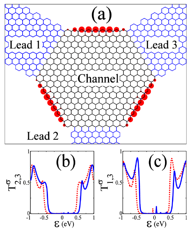
Now, we present the numerical results of spin-dependent transmission probabilities and net spin currents in three-terminal junctions with two different geometries: hexagonal (Y-shaped) and rectangular (T-shaped) structures. As shown in Fig. 1(a), in the Y-shaped junction a hexagonal-shape graphene flake (channel) with zigzag edges is sandwiched between three perfect semi-infinite armchair graphene nanoribbons (electrodes). The hexagonal channel consisting of 486 carbon atoms has the same number of A- and B-type atoms and according to Lieb’s theorem Lieb , the total magnetic moment of the ground state in the graphene flake is zero. However, by choosing an appropriate design for the electrodes in a way that the semi-infinite armchair nanoribbons are connected to only one type of carbon atoms of the channel, one can induce an imbalance in the edge magnetism between the two sublattices A and B. In this context, the total magnetic moment of the channel in Fig. 1(a) increases from zero to and, hence, a spin current without magnetic electrodes is produced. In the proposed structure the drain terminals have different widths, indicating that the rotational symmetry in the junction is broken and the transmission coefficients and spin currents in drains 1 and 2 are different.
The generation mechanism of the fully spin-polarized current relies solely on the magnetic edge states in the channel. When an unpolarized charge current flows in the channel, due to its interaction with the localized magnetic moments, it becomes spin-polarized and, hence, two spin-up and spin down currents with different transmission probabilities are generated. As a result, by using Eq. 4, we can find an appropriate electrostatic potential for electrons with energy in terminal 2 to block one of the spin currents in terminal 3. This implies that the charge current flowing in terminal 3 (see Eq. 5) is a net spin (-up or -down) current, while the both spin-up and spin-down currents in terminal 2 remain nonzero.
The spin-dependent transmission coefficients from terminal 2 to terminal 3, , and from terminal 1 to terminal 3, , as a function of electron energy, , are depicted in Figs. 1(b) and 1(c), respectively. It is shown that the transmission spectra for the two spin subbands are approximately split in the all electronic states within the shown energy windows. This feature implies that the three-terminal graphene transistor at ground state can be utilized for generation of spin-polarized currents without including spin-orbit interaction or applying magnetic fields. In other words, the separation between the two spin subbands which provide two paths for electron conduction through the junction well explains the spin-filter effect in this type of transistors. Since nonmagnetic electrodes are used in this structure, it is evident that the emergence of magnetic properties is due to the edge localized magnetic moments of the hexagonal graphene flake. Moreover, the spin-dependent transmission coefficients show various spectra around the Fermi energy, depending on the electrode thickness, so that in this structure the thicker electrode transmits electrons slightly more than the thinner one (not shown here). The transmission coefficients and have the same value due to the mirror symmetry in the junction. Note that, the transmission coefficients obey the relation at equilibrium Datta .
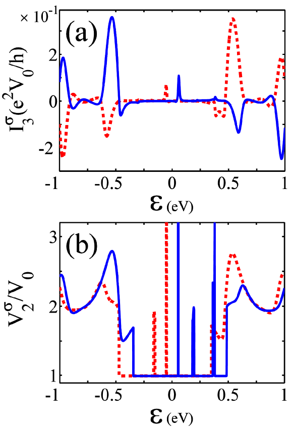
In order to achieve a fully spin-polarized current, for an electron with energy and spin the drain voltage is tuned through the constrain imposed by Eq. 4 which allows us to control the spin polarization of electrical current in the lead 3. The net spin current as a function of electron energy is shown in Fig. 2(a) when the drain voltage for the same electron energies takes the values shown in Fig. 2(b). We see that the current in lead 3 for the some energy ranges is fully spin polarized. In fact, for all electron energies at which and of Fig. 2(b) do not take the same values, a fully spin-polarized current in lead 3 is generated. In other words, if the voltage in terminal 2 takes the value , only will flow into the lead 3, while in the case of both current curves in Fig. 2(a) cross each other and this feature happens only if . Therefore, the dependence of spin currents in lead 3 on the drain voltage reveals a voltage-controlled spin transport in this type of Y-shaped transistors.
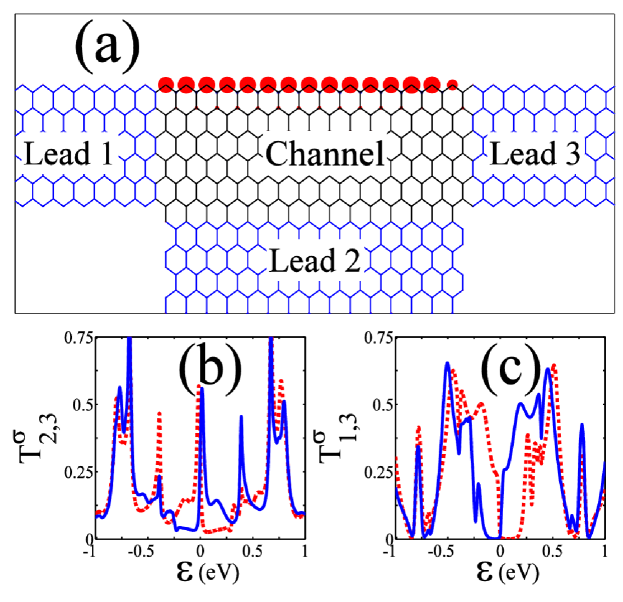
In Fig. 3(a) we consider a T-shaped junction consisting of a rectangular graphene flake (channel), sandwiched between two perfect semi-infinite zigzag nanoribbons as source (lead 1) and drain 2 (lead 3) terminals, and one semi-infinite armchair nanoribbon as drain 1 (lead 2) terminal. The rectangular channel with 180 carbon atoms has the same number of A- and B-type atoms and hence . By including the effect of semi-infinite electrodes as shown in Fig. 3(a), however, the total magnetic moment increases to . Density functional theory calculations predict that the spin-correlation length limits the long-range magnetic order to 1 nm at room temperature Yazyev . Therefore, the electron-electron interaction is limited in the channel region. In other words, the effect of induced magnetic moments on the zigzag-shaped edges in the source and drain terminals are not intentionally included in our calculations to emphasize on the role of channel geometry and its magnetic edge states in generating spin-polarized currents in such graphene nano-transistors without magnetic electrodes.
Comparing the transmission coefficients shown in Fig. 3(b) and 3(c) it is clear that due to the influence of edge states in the channel, the spectra are spin polarized and dependent on the electrode geometries. In contrast to the hexagonal junction shown in Fig. 1, the transmission coefficient of the rectangular junction does not vanish at the band center due to the zigzag-shaped edges in the source and drain terminals. The spin-dependent transmissions in such three-terminal junctions are sensitive to the width of the electrodes. The drain terminal 2 in Fig. 3(a) is wider than the other terminals. The width of terminal 2 also affects the magnitude of the induced magnetism and, hence, the generation of net spin currents becomes considerably size-dependent.
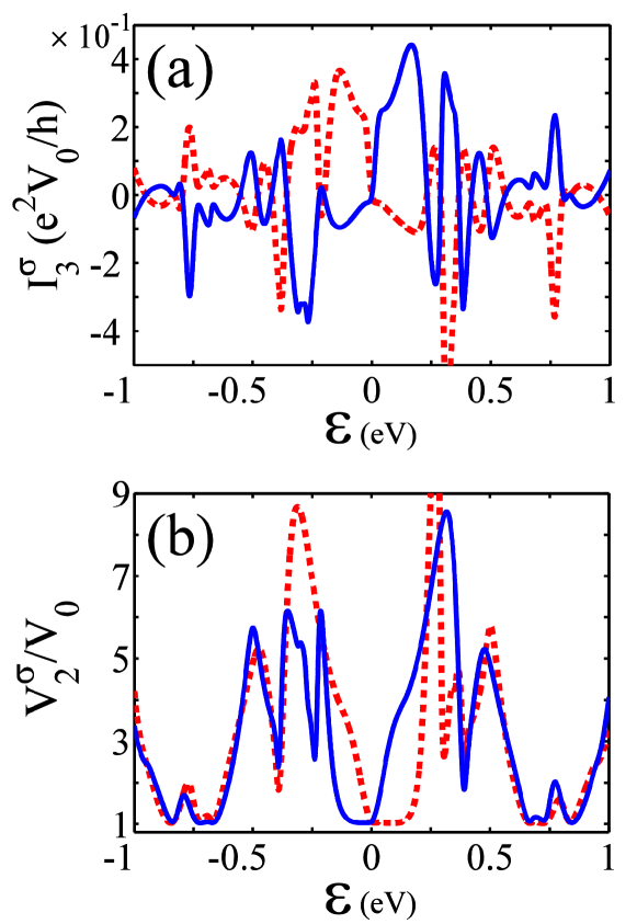
Figure 4 shows the spin-polarized electric currents in the terminal 3 and the ratio of voltages as a function of energy. The result reveals that the spin-dependent electron transport can be controlled by modulating the drain voltage 2. In addition, it is possible to alter the magnitude and the sign of spin currents if an appropriate drain voltage is chosen. In this way, the spin-dependent currents can be easily reversed and tuned between the source and drain terminals without requiring magnetic fields or electrodes, which may open a way for generation of voltage-driven spintronic devices SciRep .
Comparing Fig. 2 with Fig. 4, we find that the T-shaped structure at energies around Fermi level can function as a spin current switch in a more efficient way than the Y-shaped junction. This feature comes from zero-energy edge states Wakabayashi in the zigzag graphene nanoribbons (leads) 1 and 3 of Fig. 3(a) which act as the source and the drain terminals, respectively. In fact, at very low bias, only electrons with energies around Fermi level acquire a chance to travel from the source to the drain. Therefore, by tuning the voltage in the terminal 2, one can obtain a fully spin-polarized current (see Fig. 4(a)). Due to the absence of zero-energy edge states in the armchair graphene nanoribbons (leads) of the Y-shaped structure, a gap opens in the spin currents which vanishes the switching behavior around zero energy. Moreover, the geometry of the edges in the proposed T-shaped and Y-shaped junctions shows that the zigzag edges in the channel play the main role in the process of net spin current generation and therefore, the chirality of the leads, whether zigzag or armchair, is not crucial in the process. We should also mention that since the value of induced total magnetic moment in the Y-shaped and T-shaped junctions presented here is maximum among other three-terminal structures (not shown), it is believed that the two structures are optimal.
Note that in most three-terminal systems the spin-orbit interaction which couples the spin of electrons with their motion is the main source in generation of pure spin currents Lu ; Chi ; LWang ; Dey . Moreover, the spin-orbit interaction may lead to spin-flip scattering between electronic states with opposite spin orientations which lessens the degree of spin polarization in multi-terminal structures. In the carbon-based devices, however, the strength of intrinsic spin-orbit coupling is weak. Therefore, by designing a graphene-based three-terminal structure and utilizing the property of magnetic edge states, one can generate a net spin current without applying a magnetic field or coupling ferromagnetic leads LF ; Yamamoto ; Chi .
IV Conclusion
In conclusion, we have proposed three-terminal spin transistors based solely on carbon atoms and shown that by modulating voltage in one of the drain terminals the spin currents in the other drain terminal will be highly affected, so that a fully spin-polarized currents can be achieved. We found that the geometry of graphene flakes, the arrangement of edge atoms and the type of graphene nanoribbons taken in each terminal have significant impacts on the voltage required to generate a fully spin-polarized current. The advantage of such carbon-based spin transistors is utilizing non-magnetic electrodes which reduces manufacturing cost and the spin-dependent electron scattering. Moreover, the graphene nanoribbons are matched more conveniently to the graphene flakes and reduce the contact resistance. Therefore, the three-terminal spin devices in which the electron transmission is sensitive to the magnetic configurations of the localized moments and magnitude of the drain potentials can be an attractive pathway for designing spintronic devices with nonmagnetic electrodes.
Although the device fabrication and experimental measurement of spin currents in the well-defined zigzag edges are important challenges in this type of junctions, the Y-shaped nanoribbons Papon with zigzag edges and Y-junction carbon nanotubes Li with magnetic impurity may be experimentally useful for testing fully spin-polarized currents in such spin transistors.
Acknowledgement
This work financially supported by Iran National Support Foundation: INSF.
References
- (1) I. D. Perez, Z. Li, J. Hihath, J. Li, C. Zhang, X. Yang, L. Zang, Y. Dai, X. Feng, K. Mullen and N. Tao, Nature communication 1 31 (2010).
- (2) X. Jia, M. Hofmann, V. Meunier, B. G. Sumpter, J. Campos-Delgado, J. M. Romo-Herrera, H. Son, Y.-P. Hsieh, A. Reina, J. Kong, M. Terrones, and M. S. Dresselhaus, Science 323 1701 (2009).
- (3) F. Schwierz, Nature nanotechnology 5 478 (2010)
- (4) N. Tombros, C. Jozsa, M. Popinciuc, H. T. Jonkman and B. J. van Wees, Nature 448 2 (2007)
- (5) L. Liao,Y. C. Lin, M. Bao, R. Cheng,J. Bai, Y. Liu,Y. Qu, K. L. Wang, Y. Huang and X. Duan, Nature 467 305 (2010).
- (6) N. M. R. Peres J. Phys.: Cond. Mat. 21 32 (2009).
- (7) Y. M. Lin, C. Dimitrakopoulos, K. A. Jenkins, D. B. Farmer, H. Y. Chiu, A. Grill, Ph. Avouris, Science 327 662 (2010).
- (8) W. Y. Kim and K. S. Kim, Nature Nanotechnology 3 408 (2008).
- (9) J. Bai, R. Cheng, F. Xiu, L. Liao, M. Wang, A. Shailos, K. L. Wang, Y. Huang and X. Duan, Nature Nanotehnology 5 655 (2010).
- (10) A. R. Rocha, V. M. G. Suarez, S. W. Bailey, C. J. Lambert, J. Ferrer and S. Sanvito, Nature Materials 4 335 (2005).
- (11) S. Sugahara and J. Nitta, Proceedings of the IEEE 98 No. 12 (2010).
- (12) A. Saffarzadeh, J. Appl. Phys. 104 123715 (2008).
- (13) Y. T. Zhang, H. Jiang and Q. F. sun, Phys. Rev. B 81 165404 (2010).
- (14) V. L. J. Joly, S. J. Hao, K. Takai and T. Enoki, Phys. Rev. B 81 245428 (2010).
- (15) J. F. Rossier and J. J. Palacios, Phys. Rev. Lett. 99 177204 (2007).
- (16) M. Fujita, K. Wakabayashi, K. Nakada, and K. Kusakabe, J. Phys. Soc. Jpn. 65 1920 (1996).
- (17) J. Guo and Y. Ouyang, Appl. Phys. Lett. 94 243104 (2009).
- (18) F. M. Rojas, J. F. Rossier, and J. J. Palacios, Phys. Rev. Lett. 102 136810 (2009).
- (19) R. Farghadan and E. S. Iranizad, J. Appl. Phys. 111 014304 (2012).
- (20) S. Russo, M. F. Cracuin,Y. Yamamoto, A. F. Morpurgo and S. Tarucha, Physica E 42 677 (2010).
- (21) A. Saffrzadeh and R. Farghadan, Appl. Phys. Lett. 98 023106 (2011).
- (22) K. K. Saha, B. K. Nikolic, V. Meunier, W. Lu, and J. Bernholc Phys. Rev. Lett. 105 236803 (2010).
- (23) T. P. Pareek , Phys. Rev. Lett. 92 076601, (2004).
- (24) J. F. Liu and K. S. Chan, J. Phys. Soc. Jpn. 82 074711 (2013).
- (25) A. Brataas, Y.V. Nazarov, and G. E.W. Bauer, Phys. Rev. Lett. 84 2481 (2000).
- (26) F. Chi, J. Zheng and L-L. Sun, Appl. Phys. Lett. 92 172104 (2008).
- (27) L. G. Wang, K. Chang, and K. S. Chan, J. Appl. Phys. 105 013710 (2009).
- (28) M. Dey, S. K. Maiti, S. Sil, and S. N. Karmakar, J. Appl. Phys. 114 164318, (2013).
- (29) M. P. López Sancho, J. M. López Sancho and J. Rubio, J. Phys. F: Met. Phys. 14, 1205 (1984); 15, 851 (1985).
- (30) S. Datta, Electronic Transport in Mesoscopic Systems (Cambridge University Press, Cambridge, 1995).
- (31) M. Topsakal, V. M. K. Bagci, and S. Ciraci, Phys. Rev. B 81 205437 (2010).
- (32) E. H. Lieb, Phys. Rev. Lett. 62 1201 (1989).
- (33) O. V. Yazyev and M. I. Katsnelson, Phys. Rev. Lett. 100 047209 (2008).
- (34) W.X. Zhang , Sci. Rep. 4 6320 (2014).
- (35) K. Wakabayashi, M. Fujita, H. Ajiki, and M. Sigrist, Phys. Rev. B 59 8271 (1999).
- (36) H-F. Lü and Y. Guo, Appl. Phys. Lett. 91, 092128 (2007).
- (37) M. Yamamoto and B. Kramer , J. Appl. Phys. 103 123703 (2008).
- (38) R. Papon, S. Sharma, S. M. Shinde, A. Thangaraja, G. Kalita, and M. Tanemura, RSC Adv., 5 35297 (2015).
- (39) J. Li, C. Papadopoulos and J. Xu, Nat. 402 253 (1999).