What Makes Effective Gating Possible in Two-Dimensional Heterostructures?
Abstract
Electrostatic gating provides a way to obtain key functionalities in modern electronic devices and to qualitatively alter materials properties. While electrostatic description of such gating gives guidance for related doping effects, inherent quantum properties of gating provide opportunities for intriguing modification of materials and unexplored devices. Using first-principles calculations for Co/bilayer graphene, Co/BN, and Co/benzene, as well as a simple physical model, we show that magnetic heterostructures with two-dimensional layered materials can manifest tunable magnetic proximity effects. van der Waals bonding is identified as a requirement for large electronic structure changes by gating. In particular, the magnitude and sign of spin polarization in physisorbed graphene can be controlled by gating, which is important for spintronic devices.
Electrostatic modulation of carrier density is not only central to electronics, as in field-effect transistors (FETs), but also controls electronic phase transitions, changing an insulator into a superconductor Goldman2014:ARMS ; Ahn2006:RMP ; Ye2010:NM , or suppressing a metal-insulator transition Jeong2013:S . Such electrostatic gating is an attractive alternative to chemical doping offering reversible control of carrier density without altering the level of disorder, providing new routes in obtaining desirable materials properties. A typical range of the imposed electric field, E, to influence electronic structures can be understood from a dielectric breakdown in air V/Å and the breaking of a chemical bond V/Å estimate .
While electrostatic models Bokdam2013:PRB ; Bokdam2011:NL show important modifications from large field-induced changes of carrier density, the role of gating can be more complex with an inherent role of quantum tunneling effects Brumme2014:PRB . Electrostatic gating can profoundly alter magnetic materials by inducing ferromagnetism Zutic2004:RMP ; Yamada2011:S ; Ohno2000:N and controlling Skyrmions White2014:PRL . Field-induced redistribution of carriers can yield striking changes in the Curie temperature Cabral2011:PRB .
In this Letter we examine tunable magnetic proximity effects and reveal electric control of spin-dependent properties of nonmagnetic materials. We look for materials systems in which gating could enable large changes in the density of states (DOS) an its spin polarization.
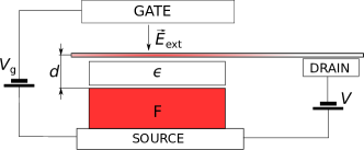
We focus on graphene (Gr)-based layered heterostructures deposited on a metallic ferromagnet (Co) as shown depicted in Fig. 1. The significance of this materials choice is two-fold: (i) such systems include van der Walls (vdW) heterostructures with unique atomically sharp interfaces Geim2013:N which simplify the implementation and characterization of electrostatic gating Ye2010:NM ; Britnell2012:S , (ii) these are key building blocks for graphene spintronics Han2014:NN with a prospect of gate-tunable magnetic proximity effects — an important precursor for lateral spin injection needed in many applications Zutic2004:RMP ; Johnson1985:PRL ; Dery2007:N ; Tombros2007:N ; Cho2007:APL ; Han2010:PRL ; Erve2012:NN ; Dery2012:IEEETED ; Lazic2014:PRB .
Even the simple effect of electrostatic screening in a metal is intrinsically quantum mechanical, as it becomes apparent from the spin-dependent screening in a ferromagnet Zhang1999:PRL ; Brovko2014:JPCM , shown in Fig. 2 for a Co slab.
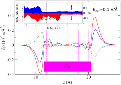
The electrostatic field is effectively screened from the interior of a metal by induced surface charges of both spin projections. However, in a ferromagnet the induced surface charge has inequivalent majority and minority spin contributions, leading to the changes of surface magnetic properties. The relative amount of these charge contributions have a quantum mechanical origin: they depend on the spin polarization of DOS, , at the Fermi level, . For Co, in which , most of the screening charge comes from the minority-spin channel Mazin1999:PRL .
What happens when we attach a nonmagnetic dielectric to a ferromagnet? Could its magnetic properties be altered? Unfortunately, there is a disconnect between many gating experiments and the lack of predictive and materials-specific methods to accurately describe them. Consequently, it is unclear what materials systems are needed to ensure that the gating will work and enable large changes in their electronic structure. Unlike conventional semiconductors in FETs, for many novel materials the corresponding screening lengths are much shorter, typically just one or two lattice constants. Electrostatic gating is therefore a surface phenomenon Goldman2014:ARMS requiring an accurate description of interfaces.
While first-principles methods provide atomically-resolved information about heterointerfaces of interest for gating experiments, standard approaches have important limitations. The use of periodic boundary conditions introduces spurious interactions with periodically repeated images of the system which needs to be corrected Gurel2013:JPCM ; Suppl . To avoid these difficulties, we implement gating Lazic2015:P in a real-space density-functional code Enkovaara2010:JPCM . For an accurate description of bonding in two-dimensional heterostructures considered here, it is crucial to include vdW interaction, which is missing in the commonly used (semi)local functionals Perdew1996:PRL . This is achieved seamlessly by using vdW-DF Dion2004:PRL , a nonlocal correlation functional Berland2014:X ; Enkovaara2010:JPCM .
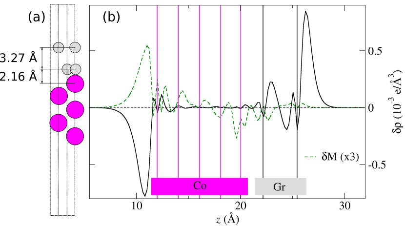
To explore the feasibility of gating in F/Gr heterostructures, we consider a Co (0001) slab attached to a bilayer Gr. The bottom Gr layer (depicted as a dielectric in Fig. 1) is chemisorbed to Co, but the top Gr layer is only weakly bound through vdW interactions. Figure 3 shows a striking difference in the response of the two Gr layers to gating. The field-induced charge rearrangement in the top Gr layer is thrice larger compared to the bottom Gr layer. Essentially, the latter is electrically grounded through strong bonding with the Co metal. In comparison with the pure Co slab (Fig. 2), spin-dependent screening in both Gr layers is negligible. Does this mean that gating can not modify the spin polarization in a nonmagnetic region?
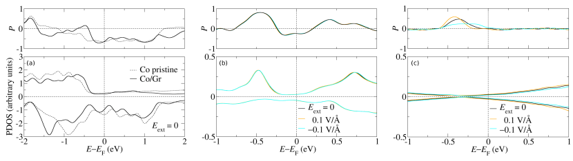
To answer this question, we examine the influence of the electric field on the layer-resolved DOS. As seen in Fig. 4, the adsorption of Gr changes the spin-dependent DOS of the top Co layer note_single . This is consistent with the expected magnetic softening of a surface Co layer from chemisorbed Gr. However, for both the pure Co slab and Gr-covered Co there are no field-induced changes in DOS. In contrast to negligible DOS changes of the bottom Gr layer [Fig. 4(b)], the changes with gating in the top layer are considerable [Fig. 4(c)]. This points to a likely trend that strongly bonded heterostructures are unsuitable for gating: the chemical bonds ground the attached dielectric to the metallic ferromagnet (Fig. 1), precluding charge transfer and control of the spin polarization. However, the top Gr layer exhibits large field-induced changes in DOS and .
Intuitively, large bonding distance could provide a large voltage drop, while small DOS suppresses screening of the external field . The resulting charge transfer for the region (top Gr layer) with a small DOS at the Fermi level will induce appreciable changes in its electronic structure. Thus, to facilitate the tunability of , one should seek an energy window with a small DOS in both spin channels. In Fig. 4(c) this is observed at V/Å for the vdW-bound top Gr layer, where the Dirac cone is largely preserved.
For practical applications, it is important to ascertain that this tunability is not unique to a specific system, and that such control of DOS and can be realized at the Fermi level. To this end, we repeated the calculations with the the bottom Gr layer replaced by hexagonal boron nitride (BN), a wide-band-gap insulator commonly used in vdW heterostructures to improve their charge and spin properties, as well as to implement topological states Geim2013:N ; Dean2010:NN ; Wang2013:S ; Guimaraes2014:PRL ; Gorbachev2014:S .
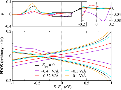
The comparison of Co/Gr/Gr and Co/BN/Gr (see Supplemental Material Suppl for computational geometry and bonding distances) in Figs. 5 and 4(c) shows that the replacement of the bottom Gr with BN preserves the overall DOS shape of the top Gr layer while slightly shifting its Dirac point. These results suggest that vdW bonding of the top Gr layer facilitates gating for two reasons: (i) It leaves the Dirac cone largely intact, maintaining a region of small DOS; (ii) This region of small DOS can be shifted in energy by , in contrast to chemical bonding which does not allow changes in DOS.
Although field-induced DOS changes seen in Fig. 5 resemble a (nonlinear in the field strength) rigid shift in energy, the behavior of is quite complicated. Similar to the small DOS region in Fig. 4(c) at eV, in Fig. 5(b) we see large changes in with near the Dirac point at eV. More importantly, large changes in are also observed [Fig. 5(c)] in the range of field magnitudes that bring the Dirac point close to . Surprisingly, the electric field changes both the magnitude and the sign of . This is a result of a complicated hybridization between Co, BN, and the two inequivalent C atoms (see Supplemental Material Suppl ).
While moderate changes [from -0.32 to -0.4 V/Å in Fig. 5(c)] lead to the changes in on the order 0.1 near , we expect that even larger changes in spin polarization could be achieved at finite bias in experiments on lateral transport. Similar trends of enhanced bias-dependent spin polarization have been studied self-consistently in magnetic p-n junctions Zutic2002:PRL .
This path towards tunable magnetic proximity effect is in contrast to the common expectations that having a magnetic insulator is required to avoid a short-circuit effect of a ferromagnetic metal Yang2013:PRL ; Wang2015:PRL ; Swartz2012:ACSN . In our approach the first attached layer is indeed grounded to the ferromagnetic metal, but the second layer offers unexplored opportunities for spintronic devices. Even common ferromagnetic metals combined with vdW bonding could provide considerable room-temperature changes in , similar to the role of MgO in achieving large tunneling magnetoresistance Zutic2004:RMP .
To predict the gating effects in systems similar to the one shown in Fig. 1, but not limited to Gr as the top layer, we formulate a simple electrostatic model. We would like to estimate the shift of the DOS for Gr relative to the ferromagnet, F (the “ground”) when an external field is applied by the gate. The simple calculation assumes energy-independent DOS, which is correct when the relative shift is small. We assume that charge can freely transfer between F and Gr over the typical time scales of the experiment (e.g. through tunneling) to establish thermodynamic equilibrium. Thus, the electrochemical potential is the same in F and Gr. When the gate voltage is applied, we then have , where are Fermi level shifts in the region (1: F; 2: Gr), and are the electrostatic potential shifts under gating. The charge density induced by the Fermi level shifts is , where is the DOS per unit area in region note_tunnel . The shifts correspond to an induced electric field between F and Gr: . Finally, the electrostatic boundary condition for Gr gives , where is the vacuum permittivity. Combining these equations, we find, using ,
| (1) |
where (and ). This corresponds to an effective dielectric constant .
We see an interesting interplay between classic electrostatics and quantum mechanics through the DOS of the gated material (). Small is required to achieve effective gating, while large is desirable.
The results of the model agree well with our calculations for Co/Gr, Co/Gr/Gr, and Co/BN/Gr structures. The DOS is an inherent property of the adsorbed top layer and a large indicates dominant vdW bonding. These findings suggests the importance of vdW bonding for effective gating. While our model is limited to layered structures, there are also non-layered vdW-bonded structures. For example, organic molecules are very promising building block for spintronics Raman2013:N .
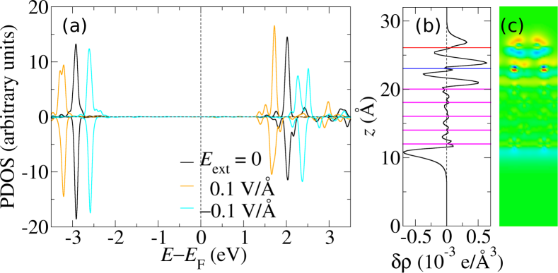
To examine the importance of the periodicity of the top vdW-bonded layer, we replace Gr by a non-periodic structure. Benzene, a dominantly vdW-bonded organic molecule, is such an example. Despite its lack of in-plane periodicity, benzene attached to Co/BN shows in Fig. 6 a very similar behavior to all the previous cases where a periodic monolayer (Gr) was attached. DOS changes with confirm effective gating, consistent with the prediction of the layered model [Eq. (1)] requiring a small DOS at of the adsorbed benzene, combined with a large vdW bonding distance. Moreover, the same vdW-bonding requirement for gating applies to absorbed single atoms, as calculated for Xe Suppl .
A weak vdW binding (physisorption) may seem incompatible with charge transfer. However, it is impossible to have “pure physisorption”with no charge rearrangement. A pure vdW attraction would bring two parts of the system together which is always prevented by the counterbalancing force due to the Pauli repulsion, known as the “push back” or “pillow” effect Bokdam2013:PRB ; Suppl . Such a charge rearrangement is indeed visible in Figs. 6(b), (c), indicating that the vdW-bound part is inevitably slightly doped.
How could the gate-controlled be experimentally detected? Perhaps the most straightforward method is the lateral spin transport. The changes of in Gr produced by the spin injector are detected by another, laterally-separated, ferromagnet Zutic2004:RMP ; Johnson1985:PRL ; Dery2007:N ; Tombros2007:N ; Cho2007:APL ; Han2010:PRL ; Erve2012:NN . It may also be possible to directly measure proximity-induced in Gr using the magneto-optical Kerr effect (MOKE) with the single F region in the geometry of Fig. 1. MOKE is capable of detecting very small spin polarizations, , and has been shown to be very sensitive in determining the structural and spin-dependent properties of Gr Ellis2013:SR . A large background from F itself could be removed using double modulation scheme Koopmans2000:PRL and lock-in amplifiers. Effectively, one would only detect the changes of in Gr corresponding to the chosen driven frequency of the gate voltage (say 1 kHz).
While we have focused on the electric control of the magnetic proximity effect, the underlying principles of effective electrostatic gating have broader implications. Many other systems are held together by vdW bonding, which, according to our first-principles calculations and a simple electrostatic model, facilitates the gating of the physisorbed part of the heterostructure. This can be already seen for gating-induced superconductivity in vdW-bonded ZrNCl Ye2010:NM and we expect it to be relevant for many vdW heterostructures, including those based on transition-metal dichalcogenides Mak2010:PRL ; Radisavljevic2011:NN . With dual gating structures, similar to the schematic from Fig. 1, carrier density and the electric field can be independently changed.
Acknowledgements.
P. L. was supported by U.S. ONR Grant N000141310754. I. Ž. was supported by U.S. DOE, Office of Science BES, under Award DE-SC0004890 (theory), NSF DMR-1124601 (applications), and the UB Center for Computational Research. K. B. acknowledges support from the Center for NanoFerroic Devices (CNFD), the Nanoelectronics Research Initiative (NRI), and NSF DMR-1308751.References
- (1) A. M. Goldman, Annu. Rev. Mater. Res. 44, 45 (2014).
- (2) C. H. Ahn et al., Rev. Mod. Phys. 78, 1185 (2006).
- (3) J. T. Ye, S. Inoue, K. Kobayashi, Y. Kasahara, H. T. Yuan, H. Shimotani and Y. Iwasa, Nat. Mater. 9, 125 (2010).
- (4) J. Jeong, N. Aetukuri,T. Graf, T. D. Schladt, M. G. Samant, and S. S. P. Parkin, Science 339, 1402 (2013).
- (5) For example, a binding of CO on Pt (111) corresponds to the binding energy 1.6 eV and a distance 2 Å.
- (6) M. Bokdam, P. A. Khomyakov, G. Brocks, and P. J. Kelly, Phys. Rev. B 87, 075414 (2013)
- (7) M. Bokdam, P. A. Khomyakov, G. Brocks, Z. Zhong, and P. J. Kelly Nano Lett. 11, 4631 (2011).
- (8) T. Brumme, M. Calandra, and F. Mauri, Phys. Rev. B 89, 245406 (2014); P. Gava, M. Lazzeri, A. M. Saitta, and F. Mauri Phys. Rev. B 79, 165431 (2009).
- (9) I. Žutić, J. Fabian, and S. Das Sarma, Rev. Mod. Phys. 76, 323 (2004).
- (10) Y. Yamada, K. Ueno, T. Fukumura, H. T. Yuan, H. Shimotani, Y. Iwasa, L. Gu, S. Tsukimoto, Y. Ikuhara, and M. Kawasaki, Science 332, 1065 (2011).
- (11) H. Ohno et al., Nature 408, 944 (2000).
- (12) J. S. White et al., Phys. Rev. Lett. 113, 107203 (2014).
- (13) E. Dias Cabral, M. A. Boselli, R. Oszwałdowski, I. Žutić, and I. C. da Cunha Lima, Phys. Rev. B 84, 085315 (2011); L. D. Anh, P. N. Hai, Y. Kasahara, Y. Iwasa, and M. Tanaka, arXiv:1503.02174, preprint.
- (14) A. K. Geim and I. V. Grigorieva, Nature (London) 499, 419 (2013).
- (15) L. Britnell, R. V. Gorbachev, R. Jalil, B. D. Belle, F. Schedin, A. Mishchenko, T. Georgiou, M. I. Katsnelson, L. Eaves, S. V. Morozov, N. M. R. Peres, J. Leist, A. K. Geim, K. S. Novoselov, and L. A. Ponomarenko, Science 335, 947 (2012).
- (16) W. Han, R. K. Kawakami, M. Gmitra, and J. Fabian, Nature Nanotech. 9, 794 (2014); C. Józsa and B. J. van Wees, in Handbook of Spin Transport and Magnetism, edited by E. Y. Tsymbal and I. Žutić (CRC Press, New York, 2011); P. Seneor, B. Dlubak, M.-B. Martin, A. Anane, H. Jaffres, and A. Fert, MRS Bull. 37, 1245 (2012).
- (17) M. Johnson, and R. H. Silsbee, Phys. Rev. Lett. 55, 1790 (1985).
- (18) H. Dery, P. Dalal, L. Cywinski, and L. J. Sham, Nature 447, 573 (2007).
- (19) N. Tombros, C. Józsa, M. Popinciuc, H. T. Jonkman, and B. J. van Wees, Nature 448, 571 (2007).
- (20) S. Cho, Y.-F. Chen, and M. S. Fuhrer, Appl. Phys. Lett. 91, 123105 (2007).
- (21) W. Han, K. Pi, K. M. McCreary, Y. Li, J. J. I. Wong, A. G. Swartz, R. K. Kawakami, Phys. Rev. Lett. 105, 167202 (2010).
- (22) O. M. J. van ’t Erve, A. L. Friedman, E. Cobas, C. H. Li, J. T. Robinson and B. T. Jonker, Nat. Nanotech. 7, 737 (2012).
- (23) H. Dery et al., IEEE Trans. Electron. Dev. 59, 259 (2012).
- (24) P. Lazić, G. M. Sipahi, R. K. Kawakami, and I. Žutić, Phys. Rev. B 90, 085429 (2014).
- (25) S. Zhang, Phys. Rev. Lett. 83, 640 (1999).
- (26) O. O Brovko, P. Ruiz-D az, T. R. Dasa, and V. S. Stepanyuk, J. Phys.: Condens. Matter 26, 093001 (2014).
- (27) In common pristine ferromagnets, there are both and . I. I. Mazin, Phys. Rev. Lett. 83, 1427 (1999).
- (28) H. Hakan Gur̈el, V. Ongun Özcelik, and S. Ciraci, J. Phys.: Condens. Matter 25, 305007 (2013).
- (29) See supplemental material for more details.
- (30) Electric fields are obtained by the state-of-the art Robin Hood electrostatic solver [P. Lazić, H. Štefančić, and H. Abraham, J. Comput. Phys. 213, 117 (2006)], suitable for an arbitrary gating electrode geometry. In this work we focus on a homogeneous electric field.
- (31) J. Enkovaara et al., J. Phys.: Condens. Matter 22, 253202 (2010).
- (32) J. P. Perdew, K. Burke, and M. Ernzerhof, Phys. Rev. Lett. 77, 3865 (1996). A widely used generalized gradient approximation predicts no binding for a bilayer graphene.
- (33) M. Dion, H. Rydberg, E. Schröder, D. C. Langreth, and B. I. Lundqvist, Phys. Rev. Lett. 92, 246401 (2004).
- (34) K. Berland, V. R. Cooper, K. Lee, E. Schröder, T. Thonhauser, P. Hyldgaard, and B. I. Lundqvist, Rep. Prog. Phys. 78, 066501 (2015).
- (35) Single Gr adsorbed on Co slab coincides in its electronic structure with bottom Gr in a bilayer adsorbed on Co slab.
- (36) C. R. Dean, A. F. Young, I. Meric, C. Lee, L. Wang, S. Sorgenfrei, K. Watanabe, T. Taniguchi, P. Kim, K. L. Shepard, and J. Hone, Nat. Nanotech. 5, 722 (2010).
- (37) L. Wang, I. Meric, P. Y. Huang, Q. Gao, Y. Gao, H. Tran, T. Taniguchi, K. Watanabe, L. M. Campos, D. A. Muller, J. Guo, P. Kim, J. Hone, K. L. Shepard, and C. R. Dean, Science 342, 614 (2013).
- (38) M. H. D. Guimarães, P. J. Zomer, J. Ingla-Aynes, J. C. Brant, N. Tombros, and B. J. van Wees, Phys. Rev. Lett. 113, 086602 (2014).
- (39) R. V. Gorbachev, J. C. W. Song, G. L. Yu, A. V. Kretinin, F. Withers, Y. Cao, A. Mishchenko, I. V. Grigorieva, K. S. Novoselov, L. S. Levitov, A. K. Geim, Science 346, 448 (2014).
- (40) I. Žutić and J. Fabian and S. Das Sarma, Phys. Rev. Lett. 88, 066603 (2002).
- (41) H. X. Yang, A. Hallal, D. Terrade, X. Waintal, S. Roche, and M. Chshiev, Phys. Rev. Lett. 110, 046603 (2013).
- (42) Z. Wang, C. Tang, R. Sachs, Y. Barlas, and J. Shi, Phys. Rev. Lett. 114, 016603 (2015).
- (43) A. G. Swartz, P. M. Odenthal, Y. Hao, R. S. Ruoff, and R. K. Kawakami, ACS Nano 6, 10063 (2012).
- (44) We do not explicitly include tunneling in this model.
- (45) K. V. Raman, A. M. Kamerbeek, A. Mukherjee, N. Atodiresei, T. K. Sen, P. Lazić, V. Caciuc, R. Michel, D. Stalke, S. K. Mandal, S. Mandal, S. Blügel, M. Munzenberg, and J. S. Moodera, Nature 493, 509 (2013).
- (46) C. T. Ellis, A. V. Stier, M-H. Kim, J. G. Tischler, E. R. Glaser, R. L. Myers-Ward, J. L. Tedesco, C. R. Eddy Jr, D. K.Gaskil, and J. Cerne, Sci. Rep. 3, 3143; DOI:10.1038/srep03143 (2013).
- (47) B. Koopmans, M. van Kampen, J. T. Kohlhepp, and W. J. M. de Jonge, Phys. Rev. Lett. 85, 844 (2000).
- (48) K. F. Mak, C. Lee, J. Hone, J. Shan, and T. F. Heinz, Phys. Rev. Lett. 105, 136805 (2010).
- (49) B. Radisavljevic, A. Radenovic, J. Brivio, V. Giacometti, and A. Kis, Nat. Nanotech. 6, 147 (2011).